Abstract
The cryogenic process and Bosch process are two widely used processes for reactive ion etching of high aspect ratio silicon structures. This paper focuses on the cryogenic deep etching of 400 nm pitch silicon gratings with various etching mask materials including polymer, Cr, SiO2 and Cr-on-polymer. The undercut is found to be the key factor limiting the achievable aspect ratio for the direct hard masks of Cr and SiO2, while the etch selectivity responds to the limitation of the polymer mask. The Cr-on-polymer mask provides the same high selectivity as Cr and reduces the excessive undercut introduced by direct hard masks. By optimizing the etching parameters, we etched a 400 nm pitch grating to ≈ 10.6 μm depth, corresponding to an aspect ratio of ≈ 53.
Index Terms: Cryogenic silicon etching, deep reactive ion etching, high aspect ratio silicon grating
I. Introduction
Etching of high aspect ratio silicon structures is a crucial step in many fabrication processes with wide applications including microelectromechanical systems (MEMS) [1], deep trench capacitors [2], through-silicon-via (TSV) packaging [3], microfluidic devices [4] and x-ray optics [5–12]. In x-ray optics, high aspect ratio gratings [5–9] and zone plates [10–12] have broad applications in x-ray phase contrast imaging [13–15], x-ray astronomy [9], and high resolution x-ray microscopy [16]. The performance of these devices relies on the aspect ratio, the size and the profile of the structures. We focus on the etching of high aspect ratio, a few hundred nm period silicon gratings. The aspect ratio is defined as the ratio between the etching depth and half pitch of the grating throughout the study. The narrow trench/wall structures of gratings impose significantly more difficulties than the etching of isolated narrow lines or trenches, since the undercut and the negative taper can damage the thin walls and closely arrayed thin walls are prone to collapse due to mutual electrostatic forces from charging effects.
Both wet and dry processes have been developed for high-aspect ratio silicon grating etching. Potassium hydroxide (KOH) etch and metal assisted chemical etch (MacEtch) are two well developed wet processes. KOH etching requires proper alignment between the trenches and the crystal orientation of a <110> silicon wafer and has been used to etch 200 nm pitch gratings down to 6 μm, corresponding to an aspect ratio of 60 [9, 17]. Vertical directionality controlled MacEtch, working with properly designed pattern and balancing structures, has been demonstrated to etch 200 nm pitch gratings down to 6.6 μm (aspect ratio of 66) [12]. Despite of certain advantages of the wet processes, we focus on dry processes. The Bosch process [18] and the cryogenic process [19] are two best known deep silicon reactive ion etching (RIE) processes [20]. Bosch process alternates isotropic etch and passivation steps to achieve directional etching. By carefully tuning the etch parameters, the intrinsic scallops on the sidewall can be reduced. The Bosch process has been used to etch 200 nm-pitch gratings to 6 μm in depth (aspect ratio of 60) [21]. The cryogenic process utilize a plasma of combined sulfur hexafluoride (SF6) and oxygen (O2) to passivate the sidewall (where a layer of SiOxFy is formed) and etch the bottom of silicon simultaneously [22–25]. The etching is typically carried out at −130 to −100 °C. The continuous process eliminates sidewall scallops and provides vertical sidewalls without observable roughness. The cryogenic process has been used to etch 200 nm pitch gratings to 4 μm in depth with regular shape and smooth sidewalls, without the need of any supporting cross bridges as has been used in the other three etching techniques [8].
Here we describe the optimization of the cryogenic recipes for high aspect ratio submicron silicon structure etching using the example of 400 nm pitch gratings. In particular, an etch mask of Cr-on-polymer was found to perform the best among several options. The effects of etching parameters [22, 23, 26, 27] and mask materials [27, 28] on cryogenic etching of silicon have been extensively studied. However, most of the studies were in the low-aspect ratio regime, under the situations of either deep etch of large micron scale structures or light etch of small nanometer scale structures [22, 23, 29]. Although valuable information has been gained, the constraints imposed by small feature size and high aspect ratio are yet to be addressed. Here we first observed the etching characteristics of different mask materials at a moderate aspect ratio of around 18. The undercut represented a severe problem for the direct hard masks and its response to the gas flow ratio (the most sensitive parameter) [22–26] was studied for the direct hard masks and Cr-on-polymer mask. Then with the Cr-on-polymer mask, the response of the etching profile to the tuning of other individual etching parameters was studied. Based on the knowledge obtained, recipes were developed for the silicon gratings to attain an aspect ratio of 53 with the Cr-on-polymer mask.
II. Methods
Figure 1 shows the cross-section scanning electron microscopy (SEM) images of the four types of grating masks with the same period of 400 nm. The polymer mask (ZEP520) was directly patterned using electron-beam lithography. Limited by the cost of electron-beam lithography, the grating area of each sample was 3 mm × 20 μm. The width of the grating line immediately above the silicon surface was ≈ 160 nm (Fig. 1A). The thickness of the resist was ≈ 540 nm. The other three masks were patterned via nanoimprint lithography with NXR-1025 nanoimprint resist (Nanonex corp.). The grating master template was a 150 mm silicon wafer, patterned via optical interference lithography and RIE of silicon. The template grating had approximately rectangular trenches of ≈ 150 nm depth. For the Cr mask, 30 nm Cr was coated on a silicon wafer via electron-beam evaporation. For the SiO2 mask, 300 nm SiO2 was first grown on a silicon wafer in a wet oxidation furnace and then 30 nm Cr was coated. The grating pattern was transferred to the spin-coated resist on silicon or Cr via nanoimprint lithography. For the Cr and the SiO2 masks, the residual layer of the nanoimprint lithography was first removed via O2 plasma, and then the 30 nm Cr was ion milled through. The Cr mask (Fig. 1B) was formed after the resist was cleaned. The SiO2 mask (Fig. 1C) was created by etching through the 300 nm SiO2 layer with a C4F8-O2 recipe and cleaning the Cr mask with O2 plasma. For the Cr-on-polymer mask (Fig. 1D), 10 nm Cr was deposited via electron beam evaporation at a 30° incident angle to the wafer surface from each side of the grating lines. The residue resist layer of the nanoimprint lithography was removed via O2 plasma. The resulting grating line widths above the silicon surface were ≈ 200 nm for all three types of masks.
Fig. 1.
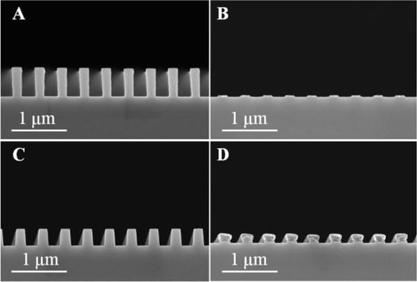
Cross-section SEM images of 400 nm period grating masks on silicon with different materials of ZEP520 (A), Cr (B), SiO2 (C) and Cr on nanoimprint resist (D).
The wafers were cleaved into 1 cm × 1 cm squares for the etching test. We also carried out an experiment with a 5 cm × 5 cm square sample masked by Cr-on-polymer, which yielded similar etching rate and profile as the smaller sample, suggesting that etching of small samples can be used to calibrate the etcher before etching large samples. The cryogenic etch process was carried out on an inductively-coupled plasma (ICP) etcher from Oxford Instruments (Oxford Plasmalab 100). The samples were bonded using pump oil on a 100 mm silicon wafer with thermally-grown SiO2 on top, which is a reliable approach for heat dissipation during the etching. The etching results were characterized by SEM.
III. Results
The cryogenic temperature was controlled to −110 ± 2 °C throughout the study. We first studied the influence of the different mask materials on the etching characteristics of 400 nm pitch gratings. The parameters of the optimized etching recipe were: ICP power of 1000 W, RF power of 10 W, pressure of 8 mT, SF6 flow rate of 52 sccm, and O2 flow rate of 8 sccm. The etching time was 2 min. Figure 2 shows the SEM images of the etching profiles corresponding to various mask materials. The depths of the trenches were 3.9, 3.8, 3.7 and 3.5 μm, the widths at the half depth were ≈ 185, 200, 190 and 205 nm for polymer, Cr, SiO2 and Cr-on-polymer masks, respectively. The slightly higher etching rate with the polymer mask was due to the slightly wider trenches. From Figs. 1 and 2, the etching selectivity was estimated to be ≈ 15, > 500, and ≈ 60 for polymer, Cr and SiO2 masks. The selectivity of the Cr-on-polymer mask was the same as Cr mask before the Cr was etched away.
Fig. 2.
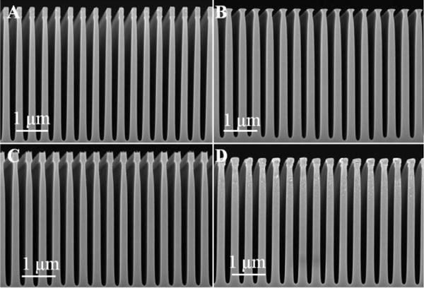
Profiles after a 2 min etch with the recipe of 1000 W ICP power, 10 W RF power, 8 mT pressure, 52 sccm SF6 and 8 sccm O2 flow rates. The mask materials are ZEP 520 (A), Cr (B), SiO2 (C) and Cr on nanoimprint resist (D).
The etch undercuts of all masks are shown in Fig. 3 by SEM of the region around the masks. The width of the polymer mask shrank from ≈ 160 nm to ≈ 125 nm for the initial 2 min of etching but did not shrink much during further etching. The smallest width of the silicon wall was almost the same as the width of the resist, indicting that the undercut was negligible for the polymer mask. More severe undercut was observed beneath the mask materials for the Cr and SiO2 masks. The undercut of the Cr-on-polymer mask was found to be close to the polymer mask for the 2 min etching. We studied the dependence of the undercut on the etching parameters for the masks of Cr, SiO2 and Cr-on-polymer and found it to be most sensitive to the SF6 and O2 flow ratio. At a fixed SF6 flow rate of 52 sccm, Fig. 4 illustrates how the undercut, the minimum silicon width at the neck and the silicon width at half depth varied with the O2 flow rate. The undercut was measured as half the difference between the silicon width immediately under the mask and the minimum width of the neck below. Figure 5 shows the corresponding etching depth. With lower O2 flow rates (< 8 sccm), the undercut increased and the width of the neck decreased rapidly for the three mask types of Cr, SiO2 and Cr-on-polymer. As a result, the sample with Cr mask did not survive a 2 min etching with 6.5 sccm O2 flow rate. With higher O2 flow rates (> 8 sccm), the undercut was reduced and the minimal width increased. Clearly increasing O2 flow rate favors the formation of the lateral etching passivation layer SiOxFy on sidewalls [30]. The trade-offs were reduced etching rate [31] and increased width at half depth, which prevent deep silicon etching. As shown in Fig. 5, the etching depth decreased monotonically with the increase of the O2 flow rate according to the increased passivation. The undercut of the Cr-on-polymer mask was substantially smaller than the Cr and SiO2 masks. We attribute this to the formation of an additional sidewall passivation layer. Carbon in the resist underneath the Cr may react to F plasma and form (CxFy)n polymer [32], through the Si etching process.
Fig. 3.
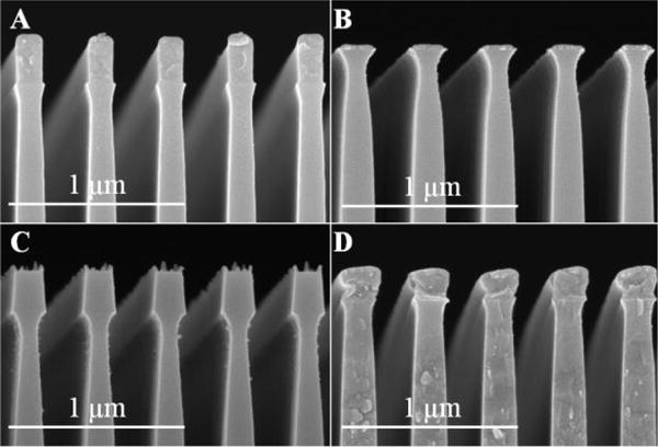
Zoomed images of the region near the masks of Fig. 2.
Fig. 4.
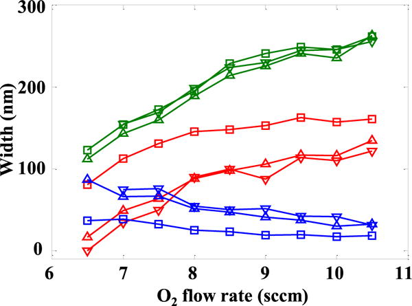
Etching characteristic widths in response to O2 flow rate for the Cr (inverted triangle), SiO2 (triangle) and Cr-on-polymer (square) masks. The blue, red and green curves represent undercut, minimum silicon width and the silicon width at half depth, respectively. The Cr masked sample did not survive 2 min etch with 6.5 sccm O2 flow rate. The minimum silicon width was taken as 0 and the other two widths are not available.
Fig. 5.
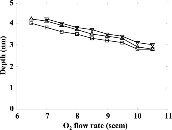
Etching depth in response to O2 flow rate for Cr (inverted triangle), SiO2 (triangle) and Cr-on-polymer (square) masks.
Since the Cr-on-polymer mask provides both good selectivity and reasonably small undercut, it allows free tuning of the other parameters. We illustrate the recipe optimization with this mask for high aspect ratio silicon grating etching. We first studied the response of etching profiles to the other etching parameters including the chamber pressure, the ICP power and the RF power with 2 min etching time. The results are summarized in Fig. 6. Figures 6A and 6B show the etching profiles at 6 mT and 15 mT chamber pressure, respectively. At 6 mT, the lower pressure increased the kinetic energy of the ion flux, thus reduced the level of passivation and straightened the sidewall of the trenches. The etching depth decreased slightly to 3.2 μm in accordance with the reduction of the ion density. The silicon width at half depth was 185 nm, the undercut was ≈ 29 nm and the slope of the sidewall was ≈ 89.5°. At 15 mT chamber pressure, the kinetic energy of the ion flux was lower and the trenches were over-passivated. As a result, the etching depth was only 1.6 μm, the undercut was 13 nm and the slope of the sidewall was ≈ 88.7°. The ICP power was set to 700 W and 1500 W. At 700 W, the plasma failed to maintain after striking at higher (2500 W) ICP power. Figure 6C shows the etching profile at 1500 W ICP power. The etching depth was 4 μm, the silicon width at the half depth was 155 nm and the undercut was 34 nm. The walls had a marginal negative taper (slope of the sidewall ≈ 90.4°) due to a slight under-passivation. The increased ion density elevated the etching speed and reduced passivation. The RF power was tuned from the initial setting of 10 W to 30 W. Figure 6D shows the etching profile at 30 W power. The etch depth was 3.5 μm. The high kinetic energy of the ion straightened the sidewall profile. As a result, the slope of the sidewall was ≈ 90.0° and the undercut was ≈ 13 nm.
Fig. 6.
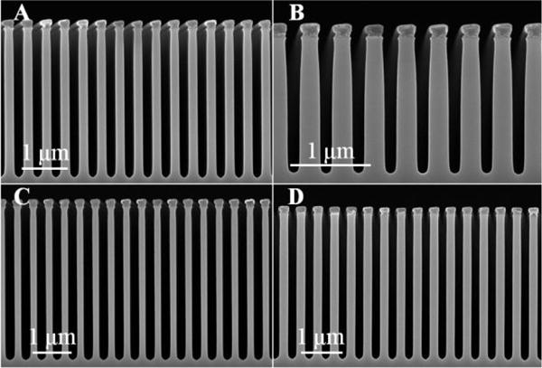
Cross-section SEM images of the samples after 2 min etching, where a single etching parameter was changed from the recipe used in Fig. 2D in each image. The tuned parameters were: (A) 6 mT chamber pressure, (B) 15 mT chamber pressure, (C) 1500 W ICP power and (D) 30 W RF power.
The overall recipe optimization involved adjusting the above parameters to balance etching against passivation within the allowance of the undercut. Choosing the optimal chamber pressure of 8 mT, we developed three recipes of different ICP and RF power combinations by adjusting the SF6 to O2 flow ratio. Figure 7A shows the etching profile of a recipe at 1000 W ICP power, 10 W RF power, 52 sccm SF6 flow rate and 8 sccm O2 flow rate. The etching time was 10 min and the etch depth was 10.6 μm, corresponding to an aspect ratio of 53. Figure 7B shows the etching profile of a recipe at 1500 W ICP power, 10 W RF power, 52 sccm SF6 and 10 sccm O2 flow rates. The etching time was 6 min and the trenches were etched to 8.3 μm depth. The slight under-passivation from higher ICP power was balanced by increasing the O2 flow rate. Although the etching rate was higher than the recipe used in Fig. 7A, the more pronounced undercut prevented further etching. Figure 7C shows the etching profile of a recipe at 1000 W ICP power, 30 W RF power, 52 sccm SF6 and 9 sccm O2 flow rates. The etching time was 6 min and the depth was 8 μm. Again, the undercut limited the achievable aspect ratio. We noted that for 2 min etching, the recipe with 30 W RF power (Fig. 6D) produced the smallest undercut. We attribute the small undercut to the removing of the silicon bumpers extended out of the mask with high energy ions. For longer etching, the recipe with 10 W RF power (Fig. 7A) gave the smallest undercut for a given etching depth.
Fig. 7.
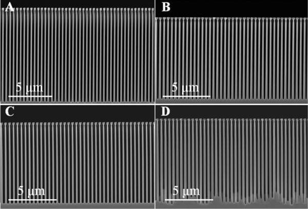
Cross-section SEM images of deeply etched samples with the Cr-on-polymer mask and recipes developed at 10 W RF power and 1000 W ICP power (A), 10 W RF power and 1500 W ICP power (B), and 30 W RF power and 1000W ICP power (C). (D) An example showing that over passivation results in uneven depths during deep silicon etching. The undercuts were estimated to be ≈ 77 nm for (A) and (B), ≈ 72 nm for (C) and ≈ 54 nm for (D).
It is worth noting that the level of passivation tends to decrease as the etch proceeds deeper, such that a slight over-passivation (positive taper) at the beginning is preferred (Fig. 2D). A recipe that starts with a vertical or negatively tapered profile results in further narrowing of the walls which are mechanically less stable and susceptible to damage before reaching the desired etch depth. On the other hand, too much passivation resulted in uneven trench depths such as the example shown in Fig. 7D, which was etched for 10 minutes using a recipe with 1000 W ICP power, 10 W RF power, 52 sccm SF6 flow rate and 10 sccm O2 flow rate.
With the recipe used in Fig. 7A, we further tested the etching characteristics of the four different masks by varying the etching time. The etching depths are illustrated in Fig. 8. The ZEP520 mask did not survive 6 min etching due to the limited thickness and selectivity. The maximum depth achieved was 6.9 μm with 5 min etching, corresponding to an aspect ratio of ≈ 35. The Cr and SiO2 masked samples did not survive 5 min etching due to the undercut. The maximum depths achieved were both 5.8 μm with 4 min etching, corresponding to an aspect ratio of 29. The undercut, the minimum silicon width near the mask and the silicon width at half depth are illustrated in Fig. 9. For polymer mask, the undercut did not change much as the etching time increased. The selectivity was the key factor that limited the achievable aspect ratio. For Cr and SiO2 masks, the undercuts increased rapidly with the etching time and the minimal silicon widths near the mask quickly dropped to below 40 nm after 4 min etching and did not allow further etching before the samples were damaged. The undercut of the Cr-on-polymer masked sample increased slowly (slightly faster than the polymer only mask) with the etching time. The high etch selectivity and moderate undercut allowed 10 min of etching, which yielded a depth of 10.6 μm, corresponding to an aspect ratio of 53.
Fig. 8.
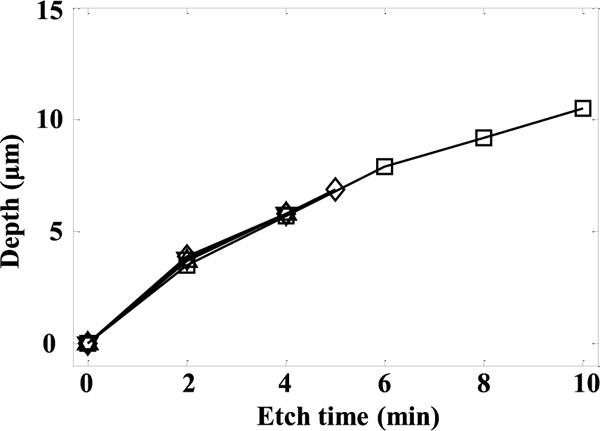
Etching depth as a function of etching time for different masks: ZEP520 (diamond), Cr (inverted triangle), SiO2 (triangle) and Cr on polymer (square).
Fig. 9.
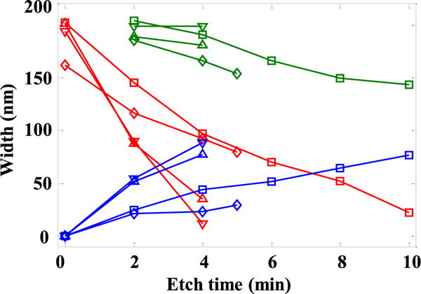
Etch characteristic widths vs the etch time for the four types of masks: ZEP 520 (diamond), Cr (inverted triangle), SiO2 (triangle) and Cr on polymer (square). The blue, red and green curves represent undercut, minimum silicon width and the silicon width at the half depth, respectively. At the start of etch the minimal silicon widths near the masks are taken as the mask widths immediately above silicon.
IV. Conclusion and Discussion
We described the cryogenic process for deep etching of 400 nm pitch silicon gratings with various mask materials. For the polymer mask, the etching selectivity of silicon over resist limits the attainable aspect ratio. For the direct hard masks of Cr and SiO2, the undercut limits the achievable aspect ratio. The Cr-on-polymer mask relaxed both constraints. We optimized the recipe for the Cr-on-polymer mask to produce gratings of an aspect ratio of 53. The optimization process was guided primarily by the balance between the etching and passivation within the tolerance of the undercut. A similar approach may be useful for developing recipes of other high aspect ratio structures in silicon.
With the Cr-on-polymer mask, the etching depth is still limited by the undercut beneath the mask. It should be noted that the etching profile of the cryogenic process is highly dependent on the feature size. For example, the recipes described here were not suitable for etching of 200 nm pitch gratings [8]. Adding a low frequency bias to the electrode might help reduce the feature size dependence of the process [22], which needs to be further investigated for high aspect ratio structures.
Acknowledgments
The authors would like to thank the National Institute of Standards and Technology, Center for Nanoscale Science and Technology where this research was conducted.
This work was supported by the the Intramural Research Program of the National Heart, Lung, and Blood Institute, National Institutes of Health.
Footnotes
Disclaimer
Certain commercial equipment, instruments, or materials are identified in this paper to specify the experimental procedure adequately. Such identification is not intended to imply recommendation or endorsement by the National Institute of Standards and Technology, nor is it intended to imply that the materials or equipment identified are necessarily the best available for the purpose.
Contributor Information
Houxun Miao, Email: houxun.miao@nih.gov, National Institutes of Health, Bethesda, MD 20892 USA.
Lei Chen, Email: lei.chen@nist.gov, National Institute of Standards and Technology, Gaithersburg, MD 20899 USA.
Mona Mirzaeimoghri, Email: mona.mirzaeimoghri@nih.gov, National Institutes of Health, Bethesda, MD 20892 USA.
Richard Kasica, Email: richard.kasica@nist.gov, National Institute of Standards and Technology, Gaithersburg, MD 20899 USA.
Han Wen, Email: han.wen@nih.gov, National Institutes of Health, Bethesda, MD 20892 USA.
References
- 1.Rangelow IW. Critical tasks in high aspect ratio silicon dry etching for microelectromechanical systems. Journal of Vacuum Science & Technology A. 2003;21:1550–1562. [Google Scholar]
- 2.Wang G, et al. Scaling deep trench based eDRAM on SOI to 32nm and Beyond,” in. Electron Devices Meeting (IEDM), 2009 IEEE International. 2009:1–4. [Google Scholar]
- 3.Motoyoshi M. Through-silicon via (TSV) Proceedings of the IEEE. 2009;97:43–48. [Google Scholar]
- 4.Verpoorte E, de Rooij NF. Microfluidics meets MEMS. Proceedings of the IEEE. 2003;91:930–953. [Google Scholar]
- 5.Noda D, et al. Fabrication of large area diffraction grating using LIGA process. Microsystem Technologies. 2008;14:1311–1315. [Google Scholar]
- 6.David C, et al. Fabrication of diffraction gratings for hard X-ray phase contrast imaging. Microelectronic Engineering. 2007;84:1172–1177. [Google Scholar]
- 7.Rutishauser S, et al. Fabrication of two-dimensional hard X-ray diffraction gratings. Microelectronic Engineering. 2013;101:12–16. [Google Scholar]
- 8.Miao H, et al. Fabrication of 200 nm Period Hard X-ray Phase Gratings. Nano letters. 2014;14:3453–3458. doi: 10.1021/nl5009713. [DOI] [PMC free article] [PubMed] [Google Scholar]
- 9.Heilmann RK, et al. Diffraction efficiency of 200-nm-period critical-angle transmission gratings in the soft x-ray and extreme ultraviolet wavelength bands. Applied optics. 2011;50:1364–1373. doi: 10.1364/AO.50.001364. [DOI] [PubMed] [Google Scholar]
- 10.Liu L, et al. Fabrication of X-ray imaging zone plates by e-beam and X-ray lithography. Microsystem Technologies. 2010;16:1315–1321. [Google Scholar]
- 11.Wojcik MJ, et al. X-ray zone plates with 25 aspect ratio using a 2-μm-thick ultrananocrystalline diamond mold. Microsystem Technologies. 2014;20:2045–2050. [Google Scholar]
- 12.Chang C, Sakdinawat A. Ultra-high aspect ratio high-resolution nanofabrication for hard X-ray diffractive optics. Nature communications. 2014;5 doi: 10.1038/ncomms5243. [DOI] [PubMed] [Google Scholar]
- 13.Pfeiffer F, et al. Phase retrieval and differential phase-contrast imaging with low-brilliance X-ray sources. Nature Physics. 2006;2:258–261. [Google Scholar]
- 14.Miao H, et al. Enhancing tabletop X-ray phase contrast imaging with nano-fabrication. Scientific Reports. 2015;5:13581. doi: 10.1038/srep13581. [DOI] [PMC free article] [PubMed] [Google Scholar]
- 15.Miao H, et al. A universal moiré effect and application in X-ray phase contrast imaging. Nature Physics. 2016 doi: 10.1038/nphys3734. doi:10.1038. [DOI] [PMC free article] [PubMed] [Google Scholar]
- 16.Chu Y, et al. Hard-x-ray microscopy with Fresnel zone plates reaches 40nm Rayleigh resolution. Applied Physics Letters. 2008;92:103119. [Google Scholar]
- 17.Ahn M, et al. Fabrication of 200 nm period blazed transmission gratings on silicon-on-insulator wafers. Journal of Vacuum Science & Technology B: Microelectronics and Nanometer Structures. 2008;26:2179–2182. [Google Scholar]
- 18.Laermer F, Schilp A. In: Plasma polymerizing temporary etch stop. Google Patents, editor. 1996. [Google Scholar]
- 19.Tachi S, et al. Low-temperature reactive ion etching and microwave plasma etching of silicon. Applied Physics Letters. 1988;52:616–618. [Google Scholar]
- 20.Wu B, et al. High aspect ratio silicon etch: A review. Journal of Applied Physics. 2010;108:051101. [Google Scholar]
- 21.Mukherjee P, et al. Plasma etch fabrication of 60: 1 aspect ratio silicon nanogratings with 200 nm pitch. Journal of Vacuum Science & Technology B. 2010;28:C6P70–C6P75. [Google Scholar]
- 22.Wu Y, et al. Cryogenic etching of nano-scale silicon trenches with resist masks. Microelectronic Engineering. 2011;88:2785–2789. [Google Scholar]
- 23.Dussart R, Tillocher T, Lefaucheux P, Boufnichel M. Plasma cryogenic etching of silicon: from the early days to today’s advanced technologies. Journal of Physics D: Applied Physics. 2014;47:123001. [Google Scholar]
- 24.Pereira J, et al. In situ X-ray photoelectron spectroscopy analysis of SiOxFy passivation layer obtained in a SF6/O2 cryoetching process. Applied Physics Letters. 2009;94:071501. [Google Scholar]
- 25.deBoer MJ, et al. Guidelines for etching silicon MEMS structures using fluorine high-density plasmas at cryogenic temperatures. Journal of Microelectromechanical Systems. 2002;11:385–401. [Google Scholar]
- 26.Tillocher T, et al. Oxidation threshold in silicon etching at cryogenic temperatures. Journal of Vacuum Science & Technology A. 2006;24:1073–1082. [Google Scholar]
- 27.Kamto A, Divan R, Sumant AV, Burkett SL. Cryogenic inductively coupled plasma etching for fabrication of tapered through-silicon vias. Journal of Vacuum Science & Technology A. 2010;28:719–725. [Google Scholar]
- 28.Sainiemi L, Franssila S. Mask material effects in cryogenic deep reactive ion etching. Journal of Vacuum Science & Technology B. 2007;25:801–807. [Google Scholar]
- 29.Liu Z, Wu Y, Harteneck B, Olynick D. Super-selective cryogenic etching for sub-10 nm features. Nanotechnology. 2013;24:015305. doi: 10.1088/0957-4484/24/1/015305. [DOI] [PubMed] [Google Scholar]
- 30.Dussart R, et al. Passivation mechanisms in cryogenic SF6/O2 etching process. Journal of Micromechanics and Microengineering. 2004;14:190–196. [Google Scholar]
- 31.d’Agostino R, Flamm DL. Plasma etching of Si and SiO2 in SF6-O2 mixtures. Journal of Applied Physics. 1981;52:162–168. [Google Scholar]
- 32.Kobayashi H, Bell AT, Shen M. Plasma polymerization of saturated and unsaturated hydrocarbons. Macromolecules. 1974;7:277–283. [Google Scholar]


