Abstract
We have investigated the local luminescence properties of Eu-doped CaAlSiN3 by using low-energy electron beam (e-beam) techniques. The particles yield broad emission centered at 655 nm with a shoulder at higher wavelength under light excitation, and a broad band around 643 nm with a tail at 540 nm under e-beam excitation. Using cathodoluminescence (CL) in a scanning electron microscope (SEM), we have observed small and large particles, which, although with different compositions, exhibit Eu2+-related emissions at 645 and 635 nm, respectively. Local CL measurements reveal that the Eu2+ emission may actually consist of several bands. In addition to the red broad band, regularly spaced sharp peaks have been occasionally observed. These luminescence variations may originate from a variation in the composition inside CaAlSiN3.
Keywords: CaAlSiN3, Eu, luminescence, electron beam, oxynitride, phosphors
1. Introduction
Field emission displays (FEDs) have received significant attention owing to their improved performance and lower power consumption compared to the actual devices, such as mercury gas-discharge fluorescence lighting or plasma displays [1–3]. The key component for FEDs is a phosphor that emits strong luminescence under electron beam (e-beam) irradiation. Actually, the most commonly used phosphors are oxides and sulfides [4–10]. However, most oxide-based phosphors have low performance, while sulfide-based ones suffer degradation under ambient atmosphere. To solve these problems, we must develop new environment-friendly phosphors with better luminescence properties, and good thermal and chemical stability.
Oxynitride materials doped with rare-earth ions are great candidates for emission applications due to excellent chemical and physical stabilities, a wide band gap and wavelength-tunable luminescence [11–16]. Indeed, the luminescence of rare-earth ions is related to their valence [17–24]. In particular, 5d–4f transitions induce broad emission bands whose positions vary with the local environment of rare-earth ions in the host lattice. Thus, some Eu-doped oxynitrides have recently shown very attractive luminescence properties, such as AlN [25], α- and β-SiAlON [26–28], M2Si5N8 and MSi2O2N2 (with M being Ca, Sr or Ba) [29–35], or CaAlSiN3 (abbreviated as CASN hereafter) [36–40].
However, due to the host-lattice and occupation site dependences, it is necessary to identify and understand the local luminescence properties of rare-earth-doped oxynitride particles. For this purpose, low-energy e-beam microscopy is useful, not only for revealing the different emission centers and their spatial distribution but also for correlating their luminescence properties with their structural and chemical ones at nanoscale [41–43]. However, few reports exist on such applications of e-beam microscopy on rare-earth-doped oxynitride phosphors [23–25, 44–52]. In this paper, we report the local luminescence properties of Eu-doped CASN by cathodoluminescence (CL) in a scanning electron microscope (SEM).
2. Experimental procedures
CASN samples were obtained by firing purchased Ca3N2 (Cerac, 99%), α-Si3N4 (Ube, Tokyo, SN-E10) and AlN (Tokuyama, Tokyo, E-Grade) and synthesized EuN at 1600 °C for 2 h and subsequently at 1800 °C for 2 h under a nitrogen pressure of 1 MPa. The synthesis details are described in [36]. The Eu concentration was fixed at 0.8%.
SEM and CL analysis were performed in a field emission SEM (Hitachi, S4300) equipped with a CL system (Horiba, MP32S/M). The beam current was fixed at 100 pA and the e-beam energy at 5 kV, which corresponds to a penetration depth of ∼ 350 nm, according to the Kanaya–Okayama model [53]. All the measurements were taken at room temperature.
Photoluminescence (PL) spectra were measured at room temperature using a fluorescence spectrophotometer (F-4500, Hitachi Ltd.) with a 150 W Ushio xenon short arc lamp.
Crystalline phases were identified by x-ray diffraction (XRD) using Cu Kα radiation (Bruker advance D8) operating at 40 kV and 40 mA.
Energy-dispersed x-ray spectroscopy (EDS) measurements were performed at room temperature in a high-resolution field emission scanning electron microscope (Hitachi, S4800). The samples were coated with Pt to reduce charging. SEM–EDS analysis was performed at 30 kV.
3. Results and discussion
Figure 1 shows the XRD pattern (a) and the EDS spectrum (b) of Eu-doped CASN. All the peaks can be attributed to CASN (JCPDS No. 39-0747) [38, 40, 54]. These peaks are sharp and intense, indicating good crystallinity. No clear secondary phase is detected. The EDS spectrum reveals peaks of C, N, O, Al, Si and Ca. No Eu peak is observed since its concentration is below the EDS detection limit. Figure 2(a) shows the CL, PL excitation and PL emission spectra of Eu-doped CASN. The PL excitation and emission spectra were recorded at 650 and 310 nm, respectively. The CL spectrum consists of a small broad band in the ultraviolet (UV) range centered at 350 nm and with a shoulder around 290 nm, and a strong band at ∼643 nm with a tail at 540 nm. The UV emissions most probably originate from defect-related luminescence from CASN or secondary phases [55–58], while the 643 nm emission is attributed to the transition from the 5d excited states to the ground state (8S7/2) of Eu2+ in CASN. The 540 nm emission may be also related to Eu2+ in CASN, but with Eu occupying a different site and/or in a different local environment. The PL emission spectrum consists of a broad band centered at 655 nm, which is 10 nm longer than that in the CL spectrum. The normalized luminescence peaks are plotted in the inset of figure 2. They show that, under e-beam excitation, the shorter wavelength emission (⩽ 640 nm) is prominent, while under optical excitation, the longer wavelength emission (≽ 650 nm) is prominent. The PL excitation consists of broad bands from 200 to 600 nm. The excitation bands in the UV region are attributed to the transition between the valence and conduction bands of the CASN host, while those in the visible region are assigned to the direct excitation of Eu2+. The differences between CL and PL emission spectra may be related to the differences in the excitation between the electron and light [59, 60]. Contrary to PL where one incident photon generates one electron–hole pair and only excites levels with lower energy than the incident photon, in the case of CL, an incident electron of energy E can generate ∼ E/3Eg, where Eg the material band gap, pairs and excites the electrons directly into the conduction band [61, 62]. Thus, PL excites just a few emission centers, while CL excites all of them. On the other hand, there may also be some absorption of the emitted green and yellow light by CASN particles themselves and their partial conversion to higher-wavelength red emission [63, 64]. Indeed, the 650 nm emission can be excited until 600 nm, as can be clearly seen in the PL excitation spectrum.
Figure 1.
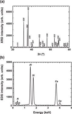
XRD pattern (a) and EDS spectrum (b) of Eu-doped CASN.
Figure 2.
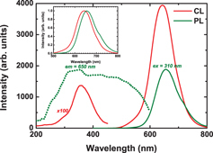
CL, PL excitation and PL emission spectra of Eu-doped CASN, with the CL and PL emission spectra normalized by their respective maximum in the inset.
Figure 3 shows the SEM (a) and CL images taken at 350 (b), 540 (c) and 640 nm (d). The Eu-doped CASN particles are relatively round, with an average size of ∼ 4 μm. The particles show some charging, but it does not noticeably affect the luminescence results. All the particles exhibit emissions at 540 and 640 nm. Interestingly, the particle edges look brighter on the 640 nm image, and darker on the 540 nm image. This may suggest that there is a compositional variation between the surface and the inner part of the particles. The 350 nm image consists of several small (∼ 1 μm) bright patches, dispersed among the particles. To see such differences in detail, we have observed the particles at higher magnification. Figure 4 shows the SEM (a) and CL images taken at 350 (b) and 640 nm (c), respectively, at higher magnification. The SEM image reveals the presence of a big particle of ∼ 4 μm and three small particles of ∼ 1 μm. As is clearly observed, the big particle shows a uniform emission at 640 nm, and the small particles at 350 nm. This suggests that the main phase CASN may coexist with a secondary phase, which was not clearly found by XRD.
Figure 3.
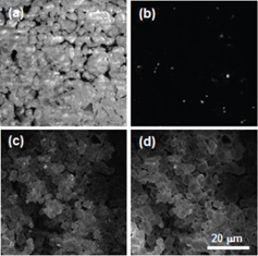
SEM (a) and CL images at 350 (b), 540 (c) and 640 nm (d) for Eu-doped CASN.
Figure 4.
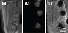
SEM (a) and CL images at 350 (b) and 640 nm (c) for Eu-doped CASN.
To confirm these results, we have performed CL and EDS measurements on the same areas to correlate the chemical and luminescence distribution. Figure 5 shows the SEM (a) and CL images taken at 350 (b) and 640 nm (c), and Al (d), Si (e) and Ca (f) distributions. The SEM and CL images are comparable to those shown in figure 3, namely consisting of big particles emitting at 640 nm and small particles emitting at 350 nm. From the EDS images, the small particles look richer in Al and weaker in Si and Ca, compared with the big particles. Namely, there is a correlation between the luminescence and the chemical distribution.
Figure 5.
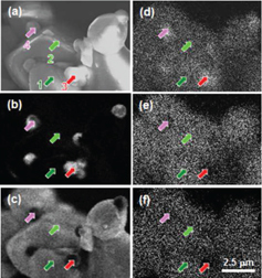
SEM (a) and CL images at 350 (b) and 640 nm (c), and Al (d), Si (e) and Ca (f) distributions for Eu-doped CASN.
To clarify these points, we have taken EDS and CL spectra on the same areas. Figure 6 shows the local EDS and CL spectra taken on areas indicated by the areas in figure 5. Points 1 and 2 were taken on big particles, while points 3 and 4 were taken on small ones. For all the EDS spectra, the peaks of C, N, O, Al, Si and Ca are observed. However, the intensities of the Al, Si and Ca peaks vary with position. Indeed, the Al and Si peak intensities are nearly the same for points 1 and 2, while the Al peak intensity is much higher than the Si one for points 3 and 4. On the other hand, the Ca peak intensity is higher for points 1 and 2 than for points 3 and 4. These spectra are in good agreement with the chemical distribution observed in figure 4. Interestingly, the EDS spectrum of point 1 is exactly the same as that of point 2, while the EDS spectra of points 3 and 4 are different from each other. These results suggest that the small particles are some secondary phase, such as an Al-rich Ca–Al–Si compound. The CL spectra for points 1 and 2 consist of a band centered at 635 nm, while those for points 3 and 4 consist of bands centered at 350 and 645 nm. The existence of the 645 nm emission from the small particles suggests that some Eu2+ ions were incorporated inside these secondary phases. The shift between the Eu2+ emission from the big and small particles may reflect the difference in the local surroundings of Eu in these two compositions. Moreover, some shoulders are observed at 545, 610, 650 and 700 nm for points 1 and 2. It may be related to a variation of the local environment of Eu in CASN and/or a difference in the occupation sites.
Figure 6.
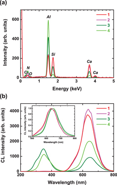
Local EDS (a) and CL spectra (b) taken on areas indicated by arrows in figure 5.
On the other hand, by performing CL analysis on local areas, we have observed another effect. Figure 7(a) shows the CL image of several CASN particles taken at 640 nm. The 640 nm emission looks uniformly distributed. No UV emission or non-radiative region is observed on these particles. Figure 7(b) shows local CL spectra taken on the areas indicated by arrows. Similarly to the CL spectra taken from the big particles (figure 4(b)), the CL spectra consist of a broad band centered at 635 nm, without any UV emission. However, contrary to the previous spectra, regularly spaced sharp peaks exist. The inset shows the enlargement of the Eu2+ emission plotted in photon energy for the spectrum taken from point 1. It is clearly seen that these peaks are regularly spaced in energy, with an interval of ∼ 50 meV. It is interesting to note that such features are not observed in every particle and that the amplitude also looks position-dependent.
Figure 7.
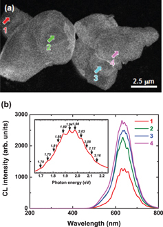
(a) CL image at 640 nm and (b) CL spectra taken on areas indicated by arrows, with the inset focusing on the Eu2+ band plotted versus photon energy.
Since the Eu2+ emission strongly depends on its local environment, the fact that the Eu2+ emission consists of several bands and that it is position dependent suggests that the CASN particles are not uniform in their composition. They may originate from an inhomogeneous distribution of Si/Al, a partial replacement of N ions by O impurities for the same crystallographic site and/or the occupation of Eu into different sites in CASN [54, 65–69]. Such changes will induce a change in the covalency, and therefore in the Stokes shift. Thus, an excited luminescent center may lose more or less energy by lattice vibration and thus emit lower- or higher-energy photons. This random luminescence distribution is in good agreement with theoretical expectations from first-principles calculations [70]. Such results may be promising for display applications. Indeed, by clarifying and controlling these local variations, we may expect to tune the emission from yellow to red in the CASN system, decrease its spectral linewidth and improve its color purity.
The ∼ 50 meV spaced sharp peaks observed during local CL measurements (figure 6) may be attributed to pseudolocalized vibrational frequency, which has always been observed for alkali halide materials [71–76]. They are attributed to defect-induced local phonons, which are related to the disorder in the materials. To the best of our knowledge, this kind of spectrum is rarely observed for SiAlON phosphors at room temperature. However, they are in good agreement with the inhomogeneous distribution found in CASN.
4. Conclusions
We have reported the luminescence of Eu-doped CASN by means of low-energy SEM-CL. Two kinds of particles were detected: 4 μm size particles emitting a large band centered at 635 nm with a shoulder at 540 nm, and 1 μm size particles emitting large bands at 290–350 and 645 nm. The large particles are identified as CASN, and the small particles as Al-rich Ca–Al–Si compounds. CL also reveals that the Eu2+ emission consists of several bands. On the other hand, ∼ 50 meV spaced sharp peaks have been observed during local CL measurements. These results suggest that the disorder in the CASN matrix greatly affects the luminescence properties. The control of such disorder may improve the tenability and color purity of CASN phosphors.
Acknowledgments
This work was supported in part by the Green Network of Excellence (GRENE) project from the Ministry of Education, Culture, Sport and Technology (MEXT) in Japan. BD is grateful for funding from the Tokodai Institute for Elemental Strategy (TIES) conducted by the Ministry of Education, Culture, Sports, Science and Technology (MEXT).
References
- Spindt C A, Holland C E, Brodie I, Mooney J B. and Westerberg E R. IEEE Trans. Electron Devices. 1988;36:225. [Google Scholar]
- Holloway P H, Trottier T A, Abrams B, Kondoleon, Jones S L, Sebastian J S, Thomes W J. and Swart H C. J. Vac. Sci. Technol. B. 1999;17:758. [Google Scholar]
- Itoh S, Tanaka M. and Tonegawa T. J. Vac. Sci. Technol. B. 2004;22:1362. [Google Scholar]
- Itoh S, Kimizuka T. and Tonegawa T. J. Electrochem. Soc. 1989;136:1819. [Google Scholar]
- Ouyang X, Kitai A H. and Xiao T. J. Appl. Phys. 1996;79:3229. [Google Scholar]
- Zhang F L, Yang S, Stoffers C, Penczek J, Yocom P N, Zaremba D, Wagner B K. and Summers C J. Appl. Phys. Lett. 1998;72:2226. [Google Scholar]
- Jiang Y D, Zhang F L, Summers C J. and Wang Z L. Appl. Phys. Lett. 1999;74:1677. [Google Scholar]
- Yang S H. and Yokoyama M. J. Vac. Sci. Technol. A. 2001;19:2463. [Google Scholar]
- Sebastian J S, Swart H C, Trottier T A, Jones S L. and Holloway P H. J. Vac. Sci. Technol. A. 1997;15:2349. [Google Scholar]
- Marsh P J, Silver J, Vecht A. and Newport A. J. Lumin. 2002;97:229. [Google Scholar]
- Feldmann C, Jüstel T, Ronda C R. and Schmidt P J. Adv. Funct. Mater. 2003;13:511. [Google Scholar]
- Xie R J. and Hirosaki N. Sci. Technol. Adv. Mater. 2007;8:588. [Google Scholar]
- Zhang M, He X, Ding W J. and Wang J. Prog. Chem. 2010;22:376. [Google Scholar]
- Xie R J, Hirosaki N, Li Y Q. and Takeda T. Materials. 2010;3:3777. [Google Scholar]
- Smet P F, Parmentier A B. and Poelman D. J. Electrochem. Soc. 2011;158:R37. [Google Scholar]
- Xie R J. and Hintzen H T. J. Am. Ceram. Soc. 2013;96:665. [Google Scholar]
- Rubio O J. J. Phys. Chem. Solids. 1991;52:101. [Google Scholar]
- Karunaratne B S B, Lumby R J. and Lewis M H. J. Mater. Res. 1996;11:2790. [Google Scholar]
- Shen Z, Nygren M. and Halenius U. J. Mater. Sci. Lett. 1997;16:263. [Google Scholar]
- van Krevel J W H, van Rutten J W T, Mandal H, Hintzen H T. and Metselaar R. J. Solid State Chem. 2002;165:19. [Google Scholar]
- Xie R J, Hirosaki N, Mitomo M, Yamamoto Y, Suehiro T. and Ohashi N. J. Am. Ceram. Soc. 2004;87:1368. [Google Scholar]
- Takahashi K, Hirosaki N, Xie R J, Harada M, Yoshimura K. and Tomomura Y. Appl. Phys. Lett. 2007;91:091923. [Google Scholar]
- Dierre B, Yuan X L, Hirosaki N, Xie R J. and Sekiguchi T. Mater. Sci. Eng. B. 2008;146:80. [Google Scholar]
- Dierre B, Yuan X L, Hirosaki N, Kimura T, Xie R J. and Sekiguchi T. J. Mater. Res. 2008;23:1701. [Google Scholar]
- Hirosaki N, Xie R J, Inoue K, Sekiguchi T, Dierre B. and Tamura K. Appl. Phys. Lett. 2007;91:061101. [Google Scholar]
- Xie R J, Hirosaki N, Sakuma K, Yamamoto Y. and Mitomo M. Appl. Phys. Lett. 2004;84:5404. [Google Scholar]
- Suehiro T, Hirosaki N, Xie R J. and Mitomo M. Chem. Mater. 2005;17:308. doi: 10.1021/jp050580s. [DOI] [PubMed] [Google Scholar]
- Hirosaki N, Xie R J, Kimoto K, Sekiguchi T, Yamamoto Y, Suehiro T. and Mitomo M. Appl. Phys. Lett. 2005;86:211905. doi: 10.1021/jp050580s. [DOI] [PubMed] [Google Scholar]
- Höppe H A, Lutz H, Morys P, Schnick W. and Seilmeier A. J. Phys.Chem. Solid. 2000;61:2001. [Google Scholar]
- Li Y Q, van Steen J E J, van Krevel J W H, Botty G, Delsing A C A, DiSalvo F J, de With G. and Hintzen H T. J. Alloys Compounds. 2006;417:273. [Google Scholar]
- Piao X Q, Horikawa T, Hanzawa H. and Machida K. Appl. Phys. Lett. 2006;88:161908. [Google Scholar]
- Piao X Q, Horikawa T, Hanzawa H. and Machida K. Chem. Lett. 2006;35:334. [Google Scholar]
- Li Y Q, Delsing A C A, de With G. and Hintzen H T. Chem. Mater. 2005;17:3242. [Google Scholar]
- Bachmann V, Ronda C, Oeckler O, Schnick W. and Meijerink A. Chem. Mater. 2009;21:316. [Google Scholar]
- Anoop G, Cho I H, Suh D W. and Yoo J S. Phys. Status Solidi a. 2012;209:2635. [Google Scholar]
- Uheda K, Hirosaki N. and Yamamoto H. Phys. Status Solidi a. 2006;203:2712. [Google Scholar]
- Uheda K, Hirosaki N, Yamamoto Y, Naito A, Nakajima T. and Yamamoto H. Electrochem. Solid-State Lett. 2006;9:H22. [Google Scholar]
- Piao X, Machida K, Horikawa T, Hanzawa H, Shimomura Y. and Kijima N. Chem. Mater. 2007;19:4592. [Google Scholar]
- Li J, Watanabe T, Wada H, Setoyama T. and Yoshimura M. Chem. Mater. 2007;19:3592. [Google Scholar]
- Lei B, Machida K, Horikawa T. and Hanzawa H. Chem. Lett. 2010;39:104. [Google Scholar]
- Gustafsson A, Pistol M E, Montelius L. and Samuelson L. J. Appl. Phys. 1998;84:1715. [Google Scholar]
- Gustafsson A. and Kapon E. Scanning Microsc. 1998;12:285. [Google Scholar]
- Dierre B, Yuan X L. and Sekiguchi T. Sci. Technol. Adv. Mater. 2010;11:043001. doi: 10.1088/1468-6996/11/4/043001. [DOI] [PMC free article] [PubMed] [Google Scholar]
- Liu X M. and Lin J. Appl. Phys. Lett. 2007;90:184108. [Google Scholar]
- Liu X M. and Lin J. J. Mater. Chem. 2008;18:221. [Google Scholar]
- Li H L, Xie R J, Hirosaki N, Dierre B, Sekiguchi T. and Yajima Y. J. Am. Ceram. Soc. 2008;91:1711. [Google Scholar]
- Dierre B, Yuan X L, Inoue K, Hirosaki N, Xie R J. and Sekiguchi T. J. Am. Ceram. Soc. 2009;92:1272. [Google Scholar]
- Liu X M. and Lin J. Solid State Sci. 2009;11:2030. [Google Scholar]
- Liu T C, Kominami H, Greer H F, Zhou W, Nakanishi Y. and Liu R S. Chem. Mater. 2012;24:3486. [Google Scholar]
- Kargin Y F, et al. Inorganic Mater. 2012;48:827. [Google Scholar]
- Xu F F, Sourty E, Zeng X H, Zhang L L, Gan L, Mou X L, Shi W, Zhu Y C, Huang F Q. and Zhai J T. Appl. Phys. Lett. 2012;101:161904. [Google Scholar]
- Dierre B, Zhang X M, Fukata N, Sekiguchi T, Suehiro T, Takeda T, Xie R J. and Hirosaki N. ECS J. Solid State. Sci. Technol. 2013;2:R126. [Google Scholar]
- Kanaya K. and Okayama S. J. Phys. D: Appl. Phys. 1972;5:43. [Google Scholar]
- Shen Y, Zhuang W, Liu Y, He H. and He T. J. Rare Earth. 2010;28:289. [Google Scholar]
- Harris J H, Youngman R A. and Teller R G. J. Mater. Res. 1990;5:1763. [Google Scholar]
- Youngman R A. and Harris J H. J. Am. Ceram. Soc. 1990;73:3238. [Google Scholar]
- Bickermann M, Epelbaum B M, Filip O, Heimann P, Nagata S. and Winnacker A. Phys. Status Solidi b. 2009;246:1181. [Google Scholar]
- Liu B D, Bando Y, Wu A M, Jiang X, Dierre B, Sekiguchi T, Tang C C, Mitome M. and Golberg D. Nanotechnology. 2010;21:075708. doi: 10.1088/0957-4484/21/7/075708. [DOI] [PubMed] [Google Scholar]
- Chen S, Dierre B, Lee W, Sekiguchi T, Tomita S, Kudo H. and Akimoto K. Appl. Phys. Lett. 2010;96:181901. [Google Scholar]
- Cueff S, Labbé C, Dierre B, Fabbri F, Sekiguchi T, Portier X. and Rizk R. J. Appl. Phys. 2010;108:113504. [Google Scholar]
- Yacobi B G and Holt D B. 1990. Cathodoluminescence Microscopy of Inorganic Solids (New York: Plenum; ) [Google Scholar]
- Yacobi B G. and Holt D B. J. Appl. Phys. 1985;59:R1. [Google Scholar]
- Dierre B, Yuan X L, Ohashi N. and Sekiguchi T. J. Appl. Phys. 2008;103:083551. [Google Scholar]
- Bulakh B, Khomenkova L, Kushnirenko V. and Markevich I. Eur. Phys. J. Appl. Phys. 2004;27:305. [Google Scholar]
- Li Y Q, Hirosaki N, Xie R J, Takeda T. and Mitomo M. Chem. Mater. 2008;20:6704. [Google Scholar]
- Lee S. and Sohn K S. Opt. Lett. 2010;35:1004. doi: 10.1364/OL.35.001004. [DOI] [PubMed] [Google Scholar]
- Yang J, Wang T, Chen D, Chen G. and Liu Q. Mater. Sci. Eng. B. 2012;177:1596. [Google Scholar]
- Park W B, Singh S P, Yoon C. and Sohn K S. J. Mater. Chem. 2012;22:14068. [Google Scholar]
- Wang T, Yang J, Mo Y, Bian L, Song Z. and Liu Q L. J. Lumin. 2013;137:173. [Google Scholar]
- Mikami M, Uheda K. and Kijima N. Phys. Status Solidi a. 2006;203:2705. [Google Scholar]
- Wagner M. and Bron W E. Phys. Rev. 1965;139:A223. [Google Scholar]
- Wagner M. and Bron W E. Phys. Rev. 1965;139:A233. [Google Scholar]
- Bron W E. Phys. Rev. 1965;140:A2005. [Google Scholar]
- Yamamoto H, Makishima S. and Shionoya S. J. Phys. Soc. Japan. 1967;23:1321. [Google Scholar]
- Meijerink A. and Blasse G. J. Lumin. 1989;43:283. [Google Scholar]
- Kang J G, Hong J P, Won S J. and Kim C O. J. Phys. Chem. Solids. 2003;64:631. [Google Scholar]


