

Abstract
The present status and recent research results on amorphous oxide semiconductors (AOSs) and their thin-film transistors (TFTs) are reviewed. AOSs represented by amorphous In–Ga–Zn–O (a-IGZO) are expected to be the channel material of TFTs in next-generation flat-panel displays because a-IGZO TFTs satisfy almost all the requirements for organic light-emitting-diode displays, large and fast liquid crystal and three-dimensional (3D) displays, which cannot be satisfied using conventional silicon and organic TFTs. The major insights of this review are summarized as follows. (i) Most device issues, such as uniformity, long-term stability against bias stress and TFT performance, are solved for a-IGZO TFTs. (ii) A sixth-generation (6G) process is demonstrated for 32″ and 37″ displays. (iii) An 8G sputtering apparatus and a sputtering target have been developed. (iv) The important effect of deep subgap states on illumination instability is revealed. (v) Illumination instability under negative bias has been intensively studied, and some mechanisms are proposed. (vi) Degradation mechanisms are classified into back-channel effects, the creation of traps at an interface and in the gate insulator, and the creation of donor states in annealed a-IGZO TFTs by the Joule heating; the creation of bulk defects should also be considered in the case of unannealed a-IGZO TFTs. (vii) Dense passivation layers improve the stability and photoresponse and are necessary for practical applications. (viii) Sufficient knowledge of electronic structures and electron transport in a-IGZO has been accumulated to construct device simulation models.
Keywords: amorphous oxide semiconductor, thin-film transistor, liquid crystal display, organic light-emitting diode display, mobility, stability, mass production
Introduction
Since our report in November 2004 on transparent and flexible thin-film transistors (TFTs) using amorphous In–Ga–Zn–O (a-IGZO), a representative amorphous oxide semiconductor (AOS) (figure 1) [1], several display companies have joined the development of this type of TFTs and have demonstrated various flat-panel displays (FPDs) including electronic papers (e-papers), organic light-emitting-diode displays (OLEDs) and liquid crystal displays (LCDs). The largest panel sizes of prototype displays reached 19″ for OLEDs [2] and 37″ for LCDs [3] as of early 2010.
Figure 1.
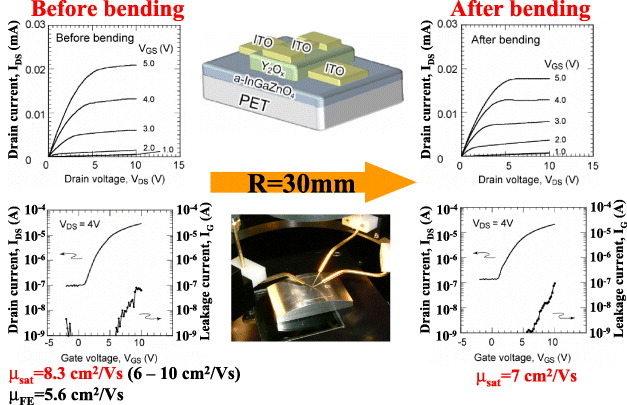
Flexible and transparent TFT using AOS fabricated on flexible PET substrate. Good TFT performance with saturation mobility above 7 cm2 V-1 s-1 is maintained even after a bending test with a curvature radius of 30 mm.
In this paper, we review the present status of AOS including their applications to FPDs and integrated circuits as well as their fundamental material science. Since we have attempted to minimize the overlap of content with preceding review papers, further details can be found in the following references. Reference [4] is for general readers and [5] contains more scientific and technical data as well as reference papers. More review papers are contained in a special issue of J. Disp. Technol. on transparent electronics [6].
The first part of this review was written with general readers in mind and will concentrate on the background and present status of oxide electronics, focusing on TFT technology. The second part overviews recent reports on scientific and technical issues related to AOS materials and their TFT characteristics, particularly focusing on a-IGZO.
Discovery of AOSs
FPDs and light-emitting diodes (LEDs), used in common electronic devices such as computers, were traditionally fabricated using conventional semiconductors such as Si, GaAs, InP and GaN. This situation changed in the late 1990 s because of intensive research on oxide conductors such as ZnO [7] for their application as active layers in semiconductor devices. A series of advances have been reported for ZnO, particularly in terms of film growth technology [8], its application in devices such as LEDs [9, 10] and the elucidation of its intrinsic properties [11], which led to demonstrations of mesoscopic effects in ZnO heterojunction systems [12] and proved that oxides can compete with conventional semiconductors (see [13] for a review).
The applications of polycrystalline ZnO (poly-ZnO) to TFTs have also been studied because poly-ZnO is known to act as an active layer in a semiconductor device even when fabricated at low temperatures below 300 °C. Therefore, ZnO is expected to replace hydrogenated amorphous silicon (a-Si:H), which is used in current FPDs. The first report on a ZnO TFT, which was fabricated in a single crystal, was published in 1968 [14], following the first proposal of a TFT fabricated using CdS in 1962 [15] and reports on TFTs fabricated using other oxides (SnO2, In2O3) [16, 17]. After a long incubation period, ZnO TFT research was revisited with many papers appearing since 2003. It is recognized that poly-ZnO TFTs still have many issues to be addressed, such as their low mobility of charge carriers and unstable electrical properties, which are largely due to grain boundaries. Another problem is the difficulty of microfabrication, which originates from their low chemical durability against acidic etchants and reducing atmospheres. There have recently been a significant improvements in these areas, and FPDs using ZnO TFT array backplanes have been demonstrated in active-matrix (AM)-LCDs by Kochi University of Technology [18, 19] and in transparent AM-OLEDs by the Electronics and Telecommunications Research Institute (ETRI) and LG Electronics (LGE) group [20, 21].
We have investigated AOSs since the mid-1990 s but from the viewpoint of fundamental materials research rather than semiconductor devices. The main objective of our research has always been to develop new functional oxide/inorganic materials, and the discovery of electrically conducting materials among amorphous oxides was a challenging topic. Until then, only a few amorphous oxide conductors had been suggested such as InOx [22] and Sn-doped In2O3 (indium tin oxide, ITO) [23], but their structures and properties were poorly characterized. We developed a materials design concept for amorphous oxide conductors and published it in 1996 [24]. We expected that the delocalized s orbitals of heavy metal cations would form a largely dispersed conduction band with a small electron effective mass, resulting in high-mobility amorphous oxide conductors. This hypothesis was proven to be correct, and many amorphous oxide conductors have since been found such as AgSbO3 [25], 2CdO·GeO2 [26], 2CdO·PbO [27], CdS·In2Sx [28] and InGaO3(ZnO)m (m⩽4) [29]. These materials were targeted for use as transparent conductive oxides and designed to have high electron density, electrical conductivity and optical transmittance.
This situation changed owing to the increasing interest in flexible electronic devices. The development of the flexible electronics was mainly driven by organic semiconductors until early 2000s, and ZnO research followed this trend. We considered the advantages and disadvantages of ZnO and organic semiconductors to be as follows. The main advantage common to these materials is that they can produce semiconductor devices as active layers even if they are deposited at low temperatures of markedly below 300 °C, whereas their main disadvantage is the instability and nonuniformity of properties due to grain boundaries. Another issue relevant to all these materials is the alteration of their electrical properties upon adsorption and desorption of trace amounts of oxygen and water. Another serious problem of ZnO and other oxide semiconductors, particularly for TFT use, is their high concentration of residual free electrons (>1017 cm-3) due to native defects such as zinc interstitials and oxygen vacancies. Consequently, it has been difficult to control the threshold voltage and to fabricate normally-off TFTs using poly-ZnO channels. To solve this problem, we employed a high-quality single-crystalline channel layer of InGaZnO4 (sc-IGZO) and demonstrated that the sc-IGZO layer does not generate a high density of residual carriers, resulting in normally-off TFTs [30]. Similarly to sc-IGZO, we found that it was difficult to dope a high density of electrons into some amorphous oxides; for instance, we had to use proton implantation to dope 2CdO·GeO2 [26]. This in turn means that the free-electron density can be stably controlled down to markedly below 1015 cm-3 using such materials including amorphous InGaO3(ZnO)m. An important advantage of amorphous materials is that they do not suffer from the grain boundary problems typical for poly-ZnO. Using these advantages, we started research on TFTs with a-IGZO channels in 2003 and reported our first results in late 2004 [1]; we demonstrated the room-temperature fabrication of transparent, flexible TFTs on polyethylene terephthalate (PET) substrates by pulsed laser deposition (figure 1). The amorphous oxides used for active layers in semiconductor devices are now known as amorphous oxide semiconductors (AOSs).
Advantages of AOSs
As explained in the Introduction, AOSs including a-IGZO are promising channel materials for TFT backplanes in FPDs because of the following features (see table 1 for a comparison with Si TFTs). AOS TFTs are compatible with the present FPD industry, which uses large inexpensive glass substrates, because they are fabricated at low temperatures below 400 °C or even at room temperature. This is the main reason why a-Si:H TFTs are used in FPDs—a-Si:H films are deposited at temperatures below 350 °C using plasma-enhanced chemical vapor deposition and SiH4 gas. However, a-Si:H has many problems such as low mobility (<1 cm2 V-1 s-1), instability under illumination (the Staebler-Wronski effect [31–33]) and electrical bias stress.
Table 1.
Comparison of a-Si:H, poly-Si and amorphous oxide TFTs.
| a-Si:H | Poly-Si | Amorphous oxide | |
|---|---|---|---|
| (LTPS/HTPS) | |||
| Generation | >10G | 4G/8G? | 8G |
| Channel | a-Si:H | ELA/SPC | a-InGaZnO4 |
| TFT masks for LCD/ OLED | (3)4–5/6–7 | 5–9/7–11 | 4–5/6–7 |
| Mobility (cm2 Vs-1) | <1 | 30–>100 | 1–20(100?) |
| TFT uniformity | Good | Poor/better | Good |
| TFT polarity | n-ch | CMOS | n-ch |
| Pixel circuit for OLED | Complex (ex. 4T2C) | Complex (ex. 5T2C) | Simple (2T+1C) |
| Cost/yield | Low/high | High/low | Low/high |
| Vth shift | >10 V | <0.5 V | <1 V |
| Light stability | Poor | Good | Superior to a-Si |
| Circuit integration | No | Yes | Yes |
| Process T | 150–350 °C | 250–550 °C | RT–400(600) °C |
| Display mode | LCD, OLED(?) | LCD, OLED | LCD, OLED, E-paper |
| Substrate | Glass, metal, (plastic) | Glass, metal, (plastic) | Glass, metal, plastic |
| Solution process, printing | No | Laser annealed | 270–400 °C |
The mobility is improved to above 10 cm2 V-1 s-1 by employing an AOS. The problem of instability was also the main concern regarding the mass production of AOSs, but recent studies have proved that the stability of a-IGZO TFTs is much greater than that of a-Si:H and organic TFTs and is comparable to that of polycrystalline silicon (poly-Si) TFTs. Poly-Si TFTs have well-known advantages over a-Si:H and organic TFTs, such as a high carrier mobility which can exceed 100 cm2 V-1 s-1 and excellent stability. It is also possible to fabricate poly-Si devices on inexpensive glass substrates by excimer laser annealing (such materials are called low-temperature poly-Si (LTPS)). However, the main drawback of poly-Si TFTs is their unacceptable variation of electrical properties due to grain boundary problems (short-range nonuniformity) [34, 35] and inhomogeneous laser crystallization over a large area (long-range nonuniformity).
These drawbacks—the low mobility and instability of a-Si:H TFTs and the poor uniformity of poly-Si TFTs—have not been critical for AM-LCDs because a low mobility of ∼0.5 cm2 V-1 s-1 is sufficient for driving the present AM-LCDs of less than 90 inches diagonal size, and the instability and nonuniformity are compensated by LCD driver circuits. However, OLEDs require high mobilities because OLED pixels emit light by electrical current injection (i.e. an OLED is a current-driving device) and TFTs must support high currents. In addition, even a small distribution or fluctuation of TFT parameters, such as threshold voltage (Vth), results in an unacceptable difference in the brightness of OLED pixels, causing a serious mura problem. For example, Jeong et al [36] reported that a variation in Vth of only ±0.1 V changes the OLED luminance by 16%. Therefore, the OLED displays using a-Si:H, poly-Si and organic TFTs reported to date must employ complex compensation circuits having four or more TFTs (e.g. 4T2C and 5T2C circuits as listed in table 1; 4T2C means that the circuit involves four transistors and two capacitors). It is believed that such TFTs will not be used in the future mass production of OLED displays.
However, the situation is changing rapidly even for AM-LCDs. It has been reported that the low-mobility a-Si:H TFTs cannot drive larger LCDs (e.g. 55 inches) operating at high frame rates above 120 Hz [37, 38]; the required mobility will be even higher for displays with higher resolution, a faster frame rate and a larger panel size (figure 2). Recently, three-dimensional (3D) displays have appeared on the market with panel sizes of ∼55 inches and frame rates of 240 Hz. However, higher frame rates of e.g. 480 Hz are required to improve the picture quality because a 3D display must project two or more picture frames alternately for the left and right eyes.
Figure 2.
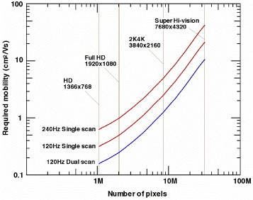
Graphical summary of required carrier mobility for future displays [38].
For these reasons, new channel materials are desired, and AOSs are expected to be one such material because they comply with all the above requirements. In particular, (i) they have high mobilities compatible with OLEDs, large LCDs and high-frame-rate 3D displays, (ii) they are compatible with large glass substrates (low-temperature fabrication) and present FPD technology, (iii) they have excellent uniformity owing to their amorphous structure and (iv) they are much more stable than a-Si:H and organic TFTs. AOS TFTs have other advantages such as the absence of a short-channel effect in small transistors [39] and the absence of the kink effect observed in crystalline silicon transistors.
Present status of displays and circuits based on AOS TFTs
Flat-panel displays
The development history of a-IGZO FPDs up to 2008 is summarized in [4] and more recent data are included in figures 3 and 4. As mentioned above, the first AOS TFT was reported in late 2004. Development research began in 2004 and Toppan Printing Co. Ltd first reported an AM display using AOS TFTs in the form of a flexible black-and-white e-paper in 2005 [40]. LGE has collaborated with ETRI on oxide TFTs and focused mainly on ZnO TFTs [20, 21]. After that, LGE started working on AOSs, and reported the first AM-OLED display in 2006 [41]. Following them, Samsung SDI and Samsung Advanced Institute of Technology (SAIT) reported AM-OLED displays in mid-2007 [42, 43]. The largest displays by the end of 2008 were a 12.1’’ AM-OLED [44, 45] and a 15’’ AM-LCD operating at 240 Hz with integrated gate drivers, as reported at the Society for Information Display (SID) meeting [46].
Figure 3.
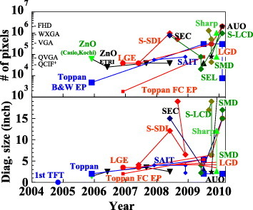
Development history of prototype displays using AOS TFTs. The panel size (diagonal size) and resolution (note that ‘# of pixels’ does not count RGB pixels separately, and is simply the product of the horizontal resolution and vertical resolution) are plotted for different companies and research groups.
Figure 4.
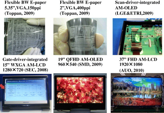
Photographs of some prototype displays using AOS TFTs. Refer to table 2 for the abbreviations of display resolutions.
From late 2008, more companies started activities involving AOSs. Hitachi Ltd, reported the low-voltage operation of AOS TFTs [47]. AU Optronics Corp. (AUO) started AOS TFT research in 2008 [48] and displayed a 2.4’’ QVGA (see table 2 for the abbreviations of the resolutions) AM-OLED at FPD International (FPDI) 2009, where a 19″ QFHD AM-OLED was reported by Samsung Mobile Display Co. Ltd (SMD) [49] and a 17″ SXGA AM-LCD by Samsung LCD. LG Display (LGD) reported a 6.4″ VGA AM-LCD, which was produced using a four-mask process similar to that used for a-Si:H LCD panels at FPDI2009, demonstrating that the production cost of AOS-based FPDs can be comparable to or even lower than those of present a-Si:H devices. Semiconductor Energy Laboratory (SEL) demonstrated source/gate driver integration in a 4″ QVGA AM-LCD [50, 51] and an AM-OLED [52]. Source/gate drive-integrated AM-LCDs were also reported by Sharp Corp. in the form of a 12.1″ WXGA AM-LCD [53]. The largest FPD driven by oxide TFTs was a 37″ FHD AM-LCD presented by AUO at TAOS2010 [3]. At the same conference, LGD reported a 15″ FHD AM-OLED [54].
Table 2.
Abbreviations and corresponding pixel resolutions appearing in section 4.1. ‘Q’ in the abbreviations indicates ‘quarter’ size of and the original resolution without ‘Q’. For example, QVGA has a resolution of 320×240 and QQVGA has that of 160×120.
| CIF | 352×288 | XGA | 1024×768 |
| QCIF+ | 176×220 | SXGA | 1280×1024 |
| (W)VGA | (800)640×480 | UXGA | 1600×1200 |
| SVGA | 800×600 | FHD | 1920×1080 |
| WQVGA | 160×272 | WXGA | 1280×720/768/800 |
Flexible displays
Flexible displays have also been reported by several companies. The first reported display was the black-and-white e-paper by Toppan [40]. They have since developed more sophisticated displays such as a black-and-white e-paper with a larger size of 5.35″ for a 150 ppi (pixel per inch) resolution and a 2″ black-and-white e-paper with the world's highest resolution of 400 ppi [55]. The first flexible FPD was an AM-OLED (3.5″, QCIF+) fabricated on stainless steel foil presented by LGE [56]. SMD reported a very flexible 6.5″ WQVGA AM-OLED fabricated on a polyimide substrate, which is bendable up to a curvature radius of 2 cm [57]. Dai Nippon Printing Co. Ltd also reported a flexible 4.7″ QVGA AM-OLED on stainless steel, which combines a white OLED and a flexible color filter array on a polyethylene naphthalene sheet [58].
Transparent displays
Another interesting application is transparent electronic devices. Toppan proposed an attractive idea that utilizes the transparency of AOS TFTs [59]. In conventional color AM e-papers and displays, a color filter array is formed on the front plane and a TFT array is formed on the back plane. Therefore, the fine alignment of these planes through liquid crystal or E-Ink microcapsules is necessary to avoid color misfit. However, the thickness of a liquid crystal is only 4–6 μm, while that of the E-Ink microcapsules is much larger (40–50 μm), which hinders the horizontal alignment. This problem is critical for flexible displays because bending the display inevitably causes misalignment of the components on the front and back planes. Toppan solved this problem by fabricating a transparent TFT array on a color filter array and integrating them into the front plane. This structure can minimize the optical transmission/reflection loss owing to the transparency of the a-IGZO TFTs.
An important application of this is expected to be in transparent displays. DENSO demonstrated a transparent monocolor passive-matrix inorganic display at FPDI2006. Toppan presented a dual-sided black-and-white display at FPDI2009. Moreover, several companies have developed transparent OLED displays. For example, LGD presented a transparent AM-OLED display having an aperture ratio of ∼30% at FPDI2009 (they claim a ∼65% aperture ratio for passive-matrix OLED), partly because they employed opaque LTPS TFT arrays. Samsung SDI reported a 4.1″ transparent dual-emission QCIF AM-OLED using a-IGZO TFTs [60], but its transparency was only ∼20%. LGE and ETRI have developed 2.5″ QCIF+ transparent OLED displays using ZnO TFT backplanes with a panel transmittance of 60% [20, 21], and they displayed a 1.5″ QQVGA transparent AM-OLED driven by AOS TFTs with a transparency of 45% at IMID2009. Transparent displays became a hot topic at SID2010; Samsung LCD displayed a 46″ transparent LCD driven by a-Si:H TFTs with an integrated touch panel and LGD presented a 47″ window TV at the exhibition. At the SID2010 conference, SMD presented a 14.1″ transparent OLED driven by LTPS TFTs with a transparency of up to 38% [61], and AUO featured a 2.4″ transparent OLED driven by a-IGZO TFTs with an integrated touch panel [62].
System integration
One of the main advantages of AOS TFTs is their high carrier mobility. This advantage is exploited in more sophisticated glass-based devices known as ‘system-on-glass (SOG)’ or ‘system-on-panel (SOP)’ devices. In these devices, electronic circuits such as pixel drivers and other peripheral circuits are integrated with TFT arrays on the same glass substrate. SEC first demonstrated a gate driver-integrated 15″ AM-LCD [46]. SEL integrated source and drain drivers in a 4″ QVGA AM-LCD [50] and an AM-OLED [51]. More recently, Sharp reported a source/driver-integrated 12.1″ AM-LCD [53]. Transparent and flexible nonvolatile memories have also been developed by several groups using a-IGZO as active layers [63–65]. These memories are expected to be integrated in AOS-based SOPs.
Production technology
Large-area fabrication techniques are required for the mass production of FPDs. Although the first AOS TFT was fabricated by pulsed laser deposition, Canon later demonstrated the fabrication of a-IGZO TFTs by radio-frequency (RF) magnetron sputtering [66]. Nowadays, most displays and AOS TFTs are fabricated by RF/dc sputtering. Some companies have attempted to develop large-size sputtering systems. For example, Oregon State University (OSU) and Applied Materials (AMAT) have been collaborating to develop metal-oxide TFTs since 2008 [67], and AKT announced a sputtering system for a 2200×2500 mm2 glass substrate at FPDI2007 (designed mainly for ITO). SEL reported a 3.4″ QHD 326 ppi AM-OLED display based on a-IGZO TFTs and fabricated by a 3.5th-generation (3.5G) process (0.6×0.72 m2; see table 3 for the glass size of different LCD process generations) [68]. AUO uses a 6G sputtering target, which was used to produce the 37″ [3] and 32″ AM-LCDs [48]. More recently, ULVAC Inc. reported the good uniformity of a-IGZO TFTs over a G4 size (0.73×0.92 m2 area) using a multicathode ac sputtering system (figure 5(a)) [69], and they also developed an 8G-size a-IGZO sputtering target (figure 5(b)). Target manufactures, such as Nippon Mining & Metals Co. Ltd, provide sputtering targets of InGaO3(ZnO)m larger than 2 m in size, which are compatible with the 8G process (figure 5(c)).
Table 3.
LCD glass size for different process generations.
| Gen. | Glass size (m2) |
|---|---|
| 1 | 0.30×0.40–0.32×0.40 |
| 2 | 0.36×0.465–0.41×0.52 |
| 3 | 0.55×0.65–0.55×0.67 |
| 3.5 | 0.59×0.67–0.65×0.83 |
| 4 | 0.68×0.88–0.73×0.92 |
| 5 | 1.00×1.20–1.20×1.30 |
| 6 | 1.50×1.80–1.50×1.85 |
| 7 | 1.87×2.10–1.95×2.25 |
| 7.5 | 1.95×2.25 |
| 8 | 2.14×2.40–2.16 ×2.40 |
| 8.5 | 2.20×2.50 |
| 10 | 2.88×3.13–3.4×2.95 |
| 11 | 3.00×3.32 |
Figure 5.
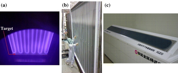
Facilities targeting mass production of AOS FPDs. (a) Multicathode AC sputtering system, and 8G-size a-IGZO sputtering targets manufactured by (b) ULVAC and (c) Nippon Mining and Metals Co. Ltd.
To minimize the fabrication cost, it is important to reduce the number of photolithography masks. The current a-Si:H LCDs employ 4–5 masks (table 4). One mask step can be eliminated by using a gray mask (also called a half-tone mask) to pattern the source/drain electrodes and the channel in a single masking step. LGD presented a 6.4″ VGA a-IGZO AM-LCD fabricated with a 4-mask process at FPDI2009, and AUO has developed a 5-mask process [71]. SMD presented a 7-mask process (table 4) [2, 72], but it was designed for an AM-OLED with an etch-stopper structure and is essentially similar to a-Si:H processes (table 1).
Table 4.
Mask steps for a-Si LCD and a-IGZO OLED.
A future critical issue is the material of bus-line electrodes. A-Si:H TFTs have used tough metals with high melting points such as Ta, Cr and Mo/Ta. Large, high-resolution and fast-frame-rate panels require higher-conducting electrodes such as Al and Cu. However, Al has poor adhesion to glass and Cu easily diffuses by electromigration as is well known in silicon ultra-large-scale integrated circuit (ULSI) technology. SEC applied Cu-based bus lines to a 15″ AMLCD [46] and AUO applied Ti/Al/Ti electrodes to 37″ AMLCD [3], in which the Ti layers improve the adhesion of the Al layer. In the case of using Cu electrodes, a group from Tohoku University examined a Cu–Mn alloy for a-IGZO TFTs and found that a self-forming MnOx layer acts as a good passivation and diffusion barrier [73]. Toppan also studied Al and Mo bus lines for e-papers because e-papers larger than 10″ will require a thick ITO layer (above 1 μm) [74].
Solution and printing processes
Other future issues are solution processes and printing technologies. These issues are thought to be the largest drawback of AOS TFTs compared with organic TFTs because, in general, oxide materials have high melting points and require high synthesis temperatures. Despite this, solution processes have been intensively studied and improved as summarized in table 5. The pioneer of this field is the HP and OSU group, who fabricated amorphous In–Zn–O (a-IZO) TFTs from halide precursors and obtained high mobilities of 16.1 cm2 V-1 s-1 for spin-coated TFTs and 7.4 cm2 V-1 s-1 for printed TFTs, however, these TFTs required a rather high annealing temperature of 400 °C [75]. SAIT has intensively studied solution processes [76] and reported the first solution-processed oxide TFT panels in the form of a 2.2″ QQVGA AM-OLED, a 4″ color QVGA LCD [77] and a single-color 4″ QVGA AM-OLED [78]. Taiwan TFT LCD Association (TTLA)/Inpria Corp./OSU also reported a 4.1″ QVGA AM-LCD [79]. They chose amorphous In–Zn–O (a-IZO) because the solution process becomes rather complex for multicomponent materials such as a-IGZO. Toppan succeeded in fabricating a high-mobility (5.4 cm2 V-1 s-1) AOS TFT at a rather low temperature of 270 °C from a solution supplied by Evonik Industries and also fabricated a 400 ppi VGA e-paper [74]. Lim et al [80] reported solution-processed a-IGZO TFTs and found that their a-IGZO films contained fine microstructures including pores. The development and selection of new precursors and the improvement of microstructure are important current issues in solution-processed AOS TFTs, and the goals are to lower the process temperature and increase the TFT mobility.
Table 5.
Previous works on solution-processed oxide semiconductors. This table is by courtesy of Dr Ito, Toppan Printing Co. Ltd. SC: spin coating, IJ: ink jet, CBD: chemical bath deposition, YIZO: Y-In-Zn-O, HIZO: Hf-In-Zn-O.
| Source | Material | Coating | Solut. type | μ (cm2 V s-1) | Temp. (°C) |
|---|---|---|---|---|---|
| B J Norris, J. Phys. D: Appl. Phys. (2003) | ZnO | SC | Precursor | 0.2 | 700 |
| H-C Cheng, Astrophys. Lett. (2007) | ZnO | SC+CBD | Precursor | 0.67 | 230 |
| B Sun, Nano Lett. (2005) | ZnO | SC | Nanorod | 0.61 | 230 |
| S T Meyers, JACS (2008) | ZnO | SC | Precursor | 1.8 | 150 |
| C Li, Astrophys. Lett. (2007) | ZnO | SC | Precursor | 0.56 | 70 |
| Y H Hwang, Electrochem. Solid State Lett. (2009) | AIO | SC | Precursor | 19.6 | 350 |
| S K Park, Electrochem. Solid State Lett. (2009) | a-ZTO | SC | Precursor | 5 | 500 |
| G H Kim, TSF (2009) | nc-IGZO | IJ | Precursor | 0.03 | 450 |
| S-Y Han, AMFPD 09 | IGZO | IJ | Precursor | 25.6 | 600 |
| In2O3 | IJ | Precursor | 11.6 | 280 | |
| H S Shin, AMFPD 09 | YIZO | SC | Precursor | 0.8 | 550 |
| S-C Chiang, SID 08 | ZnZrO | SC | Precursor | 0.0042 | 300 |
| Y-C Lai | a-IGZO | SC | Precursor | 2.1 | 450 |
| J-B Seon, IDW 09 | IZO | SC | Precursor | 6.6 | 450 |
| W H Jeong, IDW 09 | HIZO | SC | Precursor | 2 | 550 |
Section summary
The above activities indicate that AOS TFTs can be fabricated using very similar processes to those of present a-Si:H technology, and that the key technology steps, such as large-area sputtering targets and deposition systems, are being rapidly developed for their mass production. AUO announced at FINETECH JAPAN 2010 that they are ready to use a-IGZO TFTs for FPDs, and other companies also imply production of AOS-based FPDs.
Operation characteristics of a-IGZO TFTs
TFT structures and fabrication process
Hereafter, we overview the fundamental properties of a-IGZO and the operation characteristics of a-IGZO TFTs. Figure 6 illustrates typical device structures used for AOS TFTs. It is convenient to specify the TFT structure by the stacking order of the gate electrode, channel layer and source/drain electrodes (contacts) and to classify them into combinations of top/bottom gate and top/bottom contact. There is another structure called a co-planar structure in which source/drain contacts are formed in the same plane of the channel layer. This structure is employed for poly-Si TFTs and c-Si field-effect transistors (FETs), and its use has also recently been proposed for a-IGZO TFTs, as mentioned in section 5.5. The top-gate structure was employed for TFTs using epitaxial layers in which it is difficult to form a bottom electrode (e.g. c-InGaZnO4 FET [30]). This structure has other advantages. For example, it requires only two patterning mask steps at minimum, and the upper gate insulator and electrode act as passivation layers that protect the channel layer from degradation due to atmospheric exposure. Bottom-gate structures are common in laboratory research because commercially available SiO2/Si wafers can be used for the gate insulator and electrode, respectively, and TFT structures are easily formed by the deposition of a channel layer with a single mask step to form the source and drain electrodes (note that another mask step to make mesas of channel regions would be better employed to suppress the gate leakage current and prevent stray current, which often leads to the overestimation of TFT mobilities). This structure is, of course, not applicable to practical displays, and it has various disadvantages. For example, (i) the back-channel surface is exposed to the atmosphere, and therefore the TFT characteristics can be affected by the adsorption, desorption and diffusion of atmospheric gases, causing instability (section 5.8) and (ii) the gate—source/drain overlaps are very large and result in a large parasitic capacitance, which slows the response of devices and circuits. Both gate structures can employ either top-contact or bottom-contact structures. An advantage of the top-contact structure for oxide TFTs is that it can minimize the oxidation of the source/drain electrodes at the semiconductor channel interface, and geometrically accurate contacts can easily be formed. On the other hand, using a bottom-contact structure, more care is required to make good contacts with the upper channel layer, such as by forming taper-edge structures in the electrodes [66].
Figure 6.
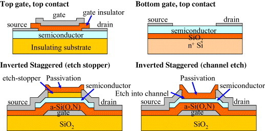
Typical device structures used for AOS TFTs.
Inverted staggered structures have been employed in most prototype displays. One reason for this is that the same structures are used for a-Si:H TFTs. These structures employ bottom-gate and top-contact configurations, which are further classified by the structure above the channel layer. One is an etch-stopper structure, where an etching protection layer is formed before forming the source and drain; the latter are patterned by etching (as proposed for a-IGZO TFTs in [81]). The other is a channel-etch structure where a part of the channel layer is removed when the source and drain are formed by etching. The channel-etching procedure damages the back-channel surface and can cause the degradation of TFT characteristics; it also requires a thick channel to stop etching in the channel layer. The etch-stopper structure is free from these problems but requires an extra patterning mask. Both structures have been employed for the mass production of a-Si:H TFTs and are also used for AOS TFTs.
TFT characteristics: Mobility
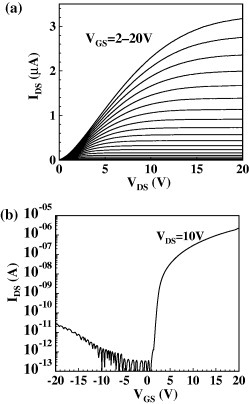
TFT characteristics are usually deduced from the output characteristics, where the source-to-drain current (IDS) is plotted against the source-to-drain voltage (VDS) for various gate-to-source voltages (VGS), and from the transfer characteristics, where IDS is plotted against VGS for various VDS, as shown in figure 7.
Figure 7.
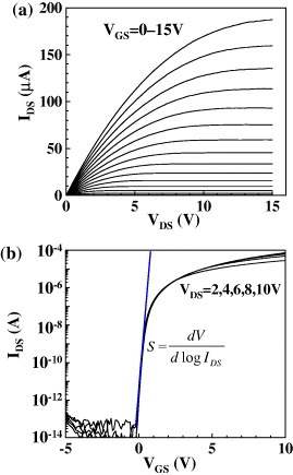
Typical output (a) and transfer (b) electrical characteristics of an a-IGZO TFT. The TFT is formed on a 150-nm-thick a-SiO2/n+-Si wafer with a top-contact structure (the dielectric constant of a-SiO2 is 3.9ε0). The TFT was annealed in air at 400 °C before forming the source/drain electrodes. The device dimensions are W/L=300/50 μm and tc=40 nm.
Device performance is evaluated in terms of several parameters as follows. On-current Ion is particularly important for current-driving devices such as OLEDs. However, Ion depends on the device geometry (i.e. channel width W, length L and thickness tc), the gate insulator material (i.e. dielectric constant εi and gate capacitance CG) and the applied voltages. Therefore, it is normalized into the field-effect (FE) mobility using an analytical equation based on the following gradual channel approximation (see [82–84] for the fundamental physics and analysis of TFTs and FETs):
Here, μ denotes the carrier mobility in the channel and Vth is a pseudo-constant called the threshold voltage. However, the observed IDS is usually lower than expected from equation (1) because defects in the channel, gate insulator and channel/gate insulator interface trap charge carriers. Therefore, the value of μ obtained from equation (1) and the experimental TFT characteristics is approximated as
Here, μd denotes the drift mobility in the channel, NGS is the total carrier density induced by VGS estimated as NGS=CG(VGS–Vth) and Nt,tot denotes the density of carriers trapped by defects. The thus-obtained μ value is called the field-effect mobility μFE (more specifically, the TFT mobility) and is used to assess the TFT performance.
Different values of μFE are obtained using different approximations as shown in figures 8(a)–(c), and it is important to check their consistency. Saturation mobility (μsat) is obtained from IDS in the saturation regime (i.e. when VDS is markedly above the pinch-off voltage Vp = VGS–Vth) under the condition VDS≫Vp using the following equation:
The values of μsat and Vth are deduced by plotting IDS1/2 versus VGS as shown in figure 8(a). Note that VDS must be larger than Vp and that there is a large deviation from linearity for low-VDS data. Even taking a large VDS of 10 V, a slight nonlinearity remains and the deduced parameters vary with μsat=8.2–12.6 cm2 V-1 s-1 and Vth=0.48–0.93 V, as indicated by the red and blue lines in figure 8.
Figure 8.
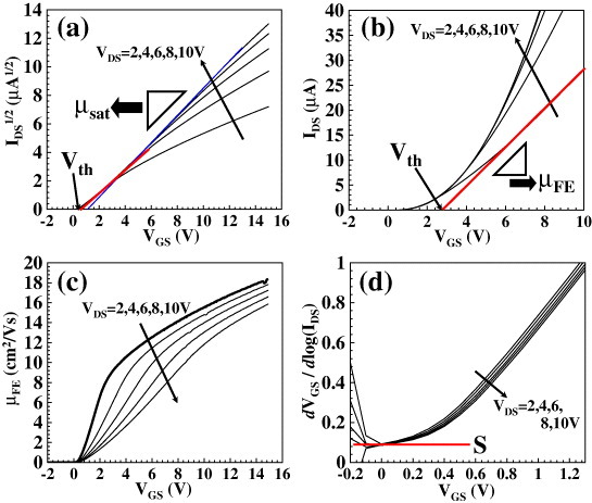
Analysis of characteristics of the a-IGZO TFT shown in figure 7. (a) Saturation mobility μsat, (b) field-effect mobility μFE, (c) μFE as a function of VGS and (d) S value. Note that only the data at VDS=10 V are valid for evaluating μsat in (a) and that VDS=2 V (the thick curve) should be used for μFE in (c).
As explained above, field-effect mobility is a general term including μsat, while it is also used as a specific definition. In this case, μFE is obtained from transfer characteristics in the linear IDS–VGS region (i.e. at VDS ∼ 0≪VGS) using the following equation:
The values of μFE and Vth are obtained by plotting IDS versus VGS as shown in figure 8(b) (13.7 cm2 V-1 s-1 and 2.63 V, respectively, using the red line). Note that VDS must be as small as possible (e.g. ≪0.1 V). Usually IDS–VGS curves are nonlinear; therefore, the value of μFE changes with VGS as shown in figure 8(c), and is represented by the maximum value (Note that only the data for VDS=2 V (the thick line) can be used for evaluating μFE because VDS must be small).
whereas crystalline Si and a-Si:H TFTs exhibit a maximum in their μFE–VGS curves [85], μFE monotonically increases up to 18 cm2 V-1 s-1 for a-IGZO. This result can be interpreted as reduction of the apparent carrier mobility due to interface scattering in the high-field region in silicon, but not in an a-IGZO TFT fabricated on an atomically flat SiO2/c-Si substrate because the interface scattering is not significant. However, maxima in μFE–VGS curves are observed in other a-IGZO TFTs, for example, in an etch-stopper-type inverted staggered TFT on glass that exhibits a large μFE of 35.8 cm2 V-1 s-1 [81]. The low values of μFE in the low-VGS region are caused by carrier trapping, as follows from equation (2).
The above analysis of a-IGZO TFT (figures 7 and 8) reveals that the two values of mobility, μsat and μFE, are consistent with each other and that the above equations are reliable for evaluating a-IGZO TFTs.
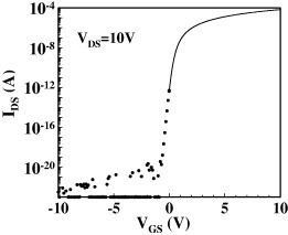
For practical applications, the off-current (Ioff) is also an important parameter because it determines the minimum power consumption of a device. Usually Ioff<10-12 A is required for FPDs, and the a-IGZO TFT shown in figure 7(b) has a much smaller value of ∼10-14 A. From the values of Ion and Ioff, the on-to-off current ratio Ron/off=Ion/Ioff is defined, which exceeds 109 for an a-IGZO TFT. The origin of Ioff is discussed in section 5.7.
TFT characteristics: subthreshold voltage swing parameter S
Another important TFT parameter is the subthreshold voltage swing (S value), which reflects the value of VGS required to obtain a 10 times larger IDS in the subthreshold region (i.e. VGS<Vth). It is defined as S=dVGS/d log10IDS. The S value is also dependent on VGS as shown in figure 8(d), and usually the smallest value of S is taken.
The importance of the S value is that it determines the minimum VGS required to turn a TFT from the off state to the on state, roughly estimated as ΔVGS,min=S×Ron/off. a-IGZO TFTs have an S value of ∼100 meV decade-1, which is comparable to that of poly-Si TFTs; this is a reason why a-IGZO TFTs operate at rather small voltages (<5 V, see figure 7).
The S value also provides important information about the quality of a TFT. It is related to the trap density in the band gap (subgap traps) at the Fermi level (Dsg) as
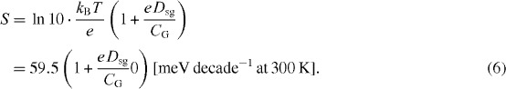 |
From this equation, the S value of a metal-insulator-semiconductor (MIS)-type FET should be larger than 59.5 mV decade-1 at 300 K and a steeper transfer curve should correspond to a higher-quality channel with fewer defects. The value of Dsg for the a-IGZO TFT described in figure 8(d) is ∼1011 cm-2eV-1. This Dsg value includes contributions from the bulk channel region Nsg and the interface Dit, and it is important to separate them to clarify the origin of the defects. A recent study reported that Dit=0.82×1011 cm-2eV-1 and Nsg=3.2×1016 cm-3eV-1 for a TFT annealed in wet oxygen at 400 °C [86]. This is discussed in section 5.8 in relation to TFT stability.
Comparison with a-Si:H TFT
Figure 9 shows the characteristics of an a-Si:H TFT. There are several differences compared with the a-IGZO TFT graphs in figure 7. In particular, (i) Ion is 1000 times smaller at ∼10-6 A, (ii) the S value is much larger at ∼0.4 V decade-1, (iii) Ioff is smaller at 10-13 A but increases with decreasing VGS and (iv) the IDS–VDS curves are nonlinear even for small VDS. As explained above, Ion and S depend on the device dimensions and should be normalized, for example, into μFE and Dsg. The above analysis yields μsat=0.24–0.60 cm2 V-1 s-1, Vth=0.2–4 V and Dsg ∼ 1012 cm-2eV-1, that is, the FE mobilities are 10 times smaller and the defect density is 10 times larger in a-Si:H TFTs than in a-IGZO TFTs. These values reflect the low mobilities of a-Si:H (∼0.8 cm2 V-1 s-1 for electrons and ∼0.002 cm2 V-1 s-1 for holes [87]). Because of the low mobilities, the present a-Si:H technology is considered unsuitable for future displays, and owing to the large defect density, a-Si:H TFTs require relatively high operating voltages.
Figure 9.
Typical output (a) and transfer (b) electrical characteristics of an a-Si:H TFT. The TFT has an inverted staggered structure with a 200-nm-thick a-SiNx:H gate insulator (dielectric constant εi=7.3ε0). The device dimensions are W/L=28/6 μm and tc=200 nm.
Electrode structures and materials
The nonlinearity of the IDS–VDS curves of the a-Si:H TFT in figure 9(a) for small VDS is caused by the large contact resistance, mostly due to the series resistance between the top source/drain electrodes and the bottom channel region (the so-called current crowding effect [88]). Similar effects have also been observed for a-IGZO TFTs, for example, in the first sputtered a-IGZO TFT [66]. The current crowding effect is examined via the channel thickness dependence in reference [89].
The nonlinearity of the IDS–VDS curves is also affected by the source/drain material and by the contact structure. We analyzed the contact resistance of various channel materials with the transmission line model [90] and found that Ti and ITO are the best electrodes [91]. The contact resistance and interface electric characteristics strongly depend on the electronic structure and carrier density of the channel surface; therefore, several treatments have been employed to improve contacts, such as Ar plasma treatment [92] and the insertion of highly doped a-IZO or a-IGZO. A drawback of oxide semiconductors is that they are easily reduced by chemical and physical treatments, such as Ar or hydrogen plasma treatment or annealing in Ar or hydrogen, but this property can also be used in a sophisticated fabrication process for co-planar homojunction TFTs [93, 94] and self-aligned processes [95–97].
It should also be noted that multilayer electrode structures such as Ti/Au (i.e. Au on Ti) and Ti/Al/Ti [3] are also used for electrodes. The Au layer protects the bottom reactive metal and decreases the contact resistivity. The Ti layer not only improves the adhesion of the top layer but also reduces the resistivity of the contact with the channel.
Subgap states and mobility model
As explained above, the S value reflects the density of subgap traps, and knowledge of this density (subgap DOS, Dsg(E)) is important for improving the TFT characteristics. Figure 10 shows a schematic Dsg(E) for a-Si:H and a-IGZO; a-Si:H has tail states below the conduction band minimum (CBM) and above the valence band maximum (VBM), and their energy dependence follows the Urbach law as Dsg(E) ∝ exp (E/Eu) (Eu is called the Urbach energy). Different values of Eu are deduced by different methods, but typically Eu ∼25 meV for the conduction band tail and Eu ∼50 meV for the valence band tail in a-Si:H. For doped a-Si:H, donor and acceptor levels also appear, and their different charge states are labeled as D-/D0/D+ in figure 10(a). A similar subgap DOS has been revealed for a-IGZO as shown in figure 10(b) [5], but there are some differences. As discussed above, S and Dsg are smaller in a-IGZO TFTs than in a-Si:H TFTs.
Figure 10.
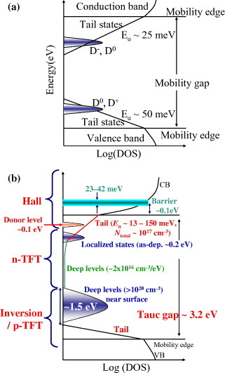
Schematic models of subgap DOS in (a) a-Si:H and (b) a-IGZO.
Reflecting this result, the subgap DOS measured by other methods such as device simulation (technology computer-assisted design, TCAD) [98] and the capacitance–voltage (C–V) method [99] substantiated that the subgap DOS in a-IGZO is one-two orders of magnitude smaller than that in a-Si:H (figure 11(a)). The C–V analysis also shows that the hysteresis in the electrical characteristics of the unannealed a-IGZO TFT (figure 11(b)) is related to an extra subgap DOS at 0.1–0.3 eV below CBM, although this energy level would be too shallow to quantitatively explain the slow response time of the hysteresis (longer than tens of seconds).
Figure 11.
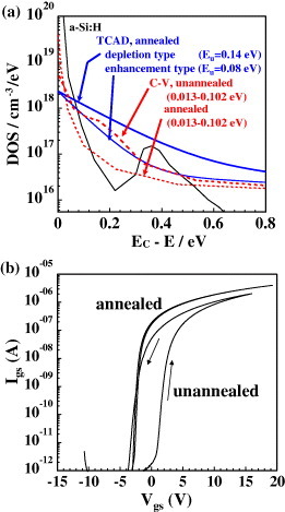
(a) Subgap DOS of a-IGZO obtained by device simulations (TCAD) and the C–V method (C–V). Depletion-type and enhancement-type a-IGZO TFTs were annealed in air at 400 °C. The DOS of a-Si:H is also shown for comparison. (b) Transfer characteristics of unannealed and annealed a-IGZO TFTs, which correspond to ‘C–V, unannealed’ and ‘annealed’ in (a), respectively.
The subgap DOS of a-IGZO varies for different a-IGZO TFTs. The larger DOS in a depletion-type TFT than in an enhancement-type TFT is explained by the larger density of donors, and thus of defect states, in the depletion-type TFT. The smaller DOS in an annealed TFT than in an unannealed TFT indicates that the annealing in air at 400 °C reduces the defect density and also annihilates the shallow defects in the 0.1–0.3 eV range, removing the hysteresis as shown in figure 11(b). The subgap DOS is separated into the interface (Dit) and the bulk (Nsg) regions (figure 12(a)), which reveals that annealing decreases Dit from 4.8×10¹¹ to 0.82×1011 cm-2 eV-1 cm-2 eV-1 and Nsg from 7.0×10¹⁶ to 3.2×1016 cm-3 eV-1 [86].
Figure 12.
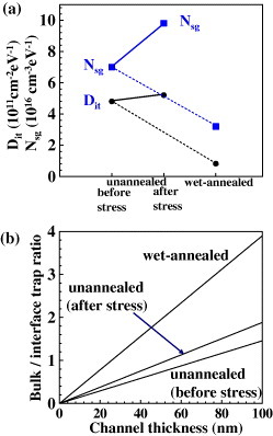
(a) Concentrations of interface (Dit, circles) and bulk defects (Nsg, squares) for unannealed and annealed a-IGZO TFTs before and after constant current stress tests, and (b) concentration ratios of bulk/surface defects, Nsgtc/Dit, as functions of channel thickness tc.
The subgap DOS of annealed a-IGZO TFTs is larger when deduced by device simulation than when deduced by the C–V method. This is because in the device simulation it is assumed that the electron mobility is constant and does not depend on carrier density, which is unrealistic as shown in figure 13(a) (the mechanism is discussed on the basis of the percolation conduction model in section 6.2, see figure 13(b)). In contrast, the C–V method does not require the assumption of the mobility model and can provide more reliable DOS data. Therefore, deducing an accurate subgap DOS and mobility model is still challenging [100]. Jeon and co-workers combined a photo-excited C–V method and device simulation and extracted the variation of effective mobility with VGS [101–104]. We also extracted the dependence of mobility on the electron density (Ne) using a combined field-effect method and found that a universal μ(Ne) model explains the different characteristics of a-IGZO TFTs subjected to different annealing treatments. The universal model follows the relation in the analytical percolation conduction model μ (Ne)=μ0 exp (−eφ eff (Ne)/kB
T) [105] with effective potential barrier height  , where φ eff0 (Ne )=φ 0−eσ φ
2 /( 2kB
T)−EBM (Ne ) is the effective barrier height measured from the Fermi level, and a1 and a2 are correction constants [106].
, where φ eff0 (Ne )=φ 0−eσ φ
2 /( 2kB
T)−EBM (Ne ) is the effective barrier height measured from the Fermi level, and a1 and a2 are correction constants [106].
Figure 13.
(a) Hall mobilities of InGaO3(ZnO)m as functions of electron density. (b) Illustration to explain the percolation conduction model. c-IGZO1 and c-IGZO5 represent crystalline phases with m = 1 and 5, respectively. HQ and LQ denote high-quality and low-quality, respectively, as defined in [107].
Deep subgap states: off current
The schematic electronic structure in figure 10(b) also shows an interesting structure above VBM. As observed in the hard x-ray photoemission spectrum (HX-PES) shown in figure 14(b), a-IGZO has a high density of occupied states above VBM with an energy width of ∼1.5 eV [107] (Note that the assignment of the valence band peaks is shown in figure 14(a), which will be compared with the density functional theory (DFT) calculation result in section 6.5). Much smaller but similar structures have also been reported in crystalline (Zn,Mg)O [108]. For a-IGZO, DFT calculations of oxygen-deficient a-IGZO suggest that a possible origin of these levels is an oxygen vacancy with a free space comparable to the size of an oxygen ion [109–111]. These deep states are important in understanding why a-IGZO TFTs do not exhibit an inversion operation, which is observed in crystalline Si FETs and also in some a-Si:H TFTs as shown in figure 9(b).
Figure 14.
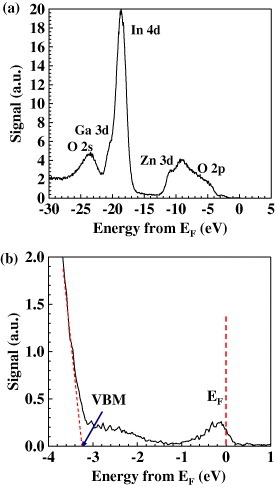
Hard x-ray photoemission spectra (HX-PES) of the (a) valence band region and (b) band-gap region. VBM is obtained by extrapolating the onset signal of the valence band spectrum as shown by the red line.
The large band gap (∼3.2 eV) [107, 109, 110] and the strongly localized valence band in a-IGZO [110] cannot explain the flat Ioff at negative VGS in figure 7(b) because the standard MIS FET model predicts that holes are induced by the inversion of band bending at negative VGS markedly below the band-gap value. Therefore, one possible explanation for the low and flat Ioff is that the source/drain contacts form a strong Schottky contact for holes and block the hole current. The device simulation in figure 15, based on the parameters and the subgap DOS model in [98], reveals that Ioff should be <10-20 A for an ideal TFT, which should be due to the Schottky contact for holes.
Figure 15.
Simulated transfer curve of a-IGZO TFT. The parameters are taken from [98]. The scatter in the reverse-bias currents is due to their extremely low values.
However, it is difficult to believe that oxide semiconductors form a stable and good Schottky contact [112–114], because oxide semiconductor–metal contacts easily exhibit an ohmic behavior, which is explained by the formation of conductive layers by a reduction reaction [115]. As is known for poly-Si TFTs, direct contact between an electrode and a channel results in a strong electric field at the interface and causes a leakage current due to tunneling, hot electron injection and generation-recombination current by the Shockley–Reed–Hall (SRH) mechanism; therefore, a lightly doped drain structure is employed. A similar mechanism should apply to a-IGZO TFTs; although the band gap is much larger for a-IGZO, the SRH mechanism can still be efficient owing to the surface reduction layer having a high density of defect states.
The deep-subgap DOS above VBM in figure 14(b) provides another possible explanation of the low Ioff. The subgap DOS extends up to ∼1.5 eV above VBM, and its density exceeds 1020 cm-3 even for high-quality, weakly doped a-IGZO films [116]. This density is larger than the electron density that can be induced by VGS (<1018 cm-3), as estimated from the relation Ne ∼CG·VGS/e based on the TFT dimensions in figure 7. In such a case, the Fermi level is pinned in the subgap DOS and thus there should be no mobile holes in the valence band. According to a recent angle-resolved hard x-ray photoemission spectroscopy (AR-HX-PES) study, the deep part of the DOS is mostly concentrated in the surface region [116], but it still remains a possible origin of the pinning centers because the detection limit of HX-PES is above 1019 cm-3, and such a density is still sufficiently high to pin the Fermi level in conventional TFT structures.
Figure 14(b) shows the peak structure around the Fermi energy EF, suggesting that a high density of electrons exists near the conduction band. Similar structures have been reported in highly doped a-IZO [117] and can be attributed to doped electrons. We estimate the corresponding densities to be >5×10¹⁹, but these values are larger than the carrier density that can be induced by VGS and cannot be achieved in TFTs. The AR-HX-PES results showed no systematic relationship between the shallow DOS and the electron density measured using the Hall effect [116].
Stability
The long-term stability and reliability of TFTs are the most important issues for their mass production. The stability of AOS TFTs has been intensively studied in recent years. As mentioned above, a-IGZO TFTs have high mobilities of above 10 cm2 V-1 s-1 even when fabricated at room temperature; however, the uniformity and stability are poor for unannealed TFTs [118, 119]. Therefore, most a-IGZO TFTs in prototype displays have been annealed at a temperature above 300 °C (lower annealing temperatures have been applied recently). We reported that such high-temperature annealing is necessary to oxidize a-IGZO and reduce the concentration of native donor defects in as-deposited a-IGZO, even in a pure O2 atmosphere; electrical conductivity increases with annealing temperature up to ∼300 °C and then starts decreasing [118]. This result indicates that O2 molecules do not have sufficient oxidizing power to passivate the defects in a-IGZO below 300 °C. We also found that annealing is more effective in wet oxygen than in dry oxygen, which was attributed to the stronger oxidation power provided by H2O molecules. Thermal annealing removes weak chemical bonds, particularly Zn–O-related bonds, and forms stable a-IGZO. Constant-current stress tests revealed that annealed a-IGZO TFTs are much more stable than unannealed TFTs with the saturation values of the Vth shift (ΔVth) less than 2 V [119].
Some groups, including ours, have reported that the time dependence of ΔVth follows a stretched exponential law [120, 121]. Most results of ΔVth under bias stress tests exhibit a positive shift, which is explained by the following contributions: the trapping of positive charges in (i) the gate insulator, (ii) the channel-gate insulator interface, (iii) the bulk of the channel and (iv) the back-channel surface, as well as (v) the creation of acceptor-type deep traps (i.e. unoccupied defects that can accept extra electrons) and (vi) a decrease in the donor concentration. Contribution (vi) can be ruled out because it is difficult to believe that the defect density can decrease during a degradation test. Regarding to our studies [86, 119], contribution (i) can also be excluded because we used stable thermally oxidized SiO2 formed on a Si wafer. But this mechanism is valid for other practical device structures that employ SiO2, SiON or SiNx gate insulators and are not formed by high-temperature oxidation of single-crystalline silicon.
There have been reports of other ΔVth(t) dependences. An exponential dependence of ΔVth(t) has been reported for a constant–voltage stress test and explained by charge tunneling [122]. It is pointed out that most of the instability of bottom-gate a-IGZO TFTs with the back-channel surface exposed to the atmosphere originates from the adsorption/desorption of oxygen and water molecules [123, 124]; they proposed a field-induced adsorption/desorption model [125].
The instability due to the exposed back channel is solved by adopting dense, gas-tight passivation layers (see, for example, [126]) and employing a top-gate structure in which the gates act as passivation layers [127]. Actually, most of the recent a-IGZO TFTs have employed passivation layers made of SiO2 [128], SiNx [93], Al2O3 [129, 130] or TiOx [3, 131]. It has also been found that the transfer characteristics of annealed a-IGZO TFTs under bias stress tests only exhibit parallel shifts; i.e. the values of S and mobility are not affected. This behavior is explained by the formation of deep traps, which reduce the density of free electrons in the channel.
We reported that this situation is different for unannealed TFTs fabricated at room temperature, which also exhibit the degradation of S values, and that the increase in the subgap DOS near CBM must also be considered [119]. This degradation is recovered by aging at room temperature in air for over 10 h [132]. We also observed that only applying negative-bias stress does not change Vth. The instability against positive bias stress discussed above and the high stability against negative-bias stress suggest that the positive-bias instability is related to the current flow. Uraoka and co-workers observed Joule heating by the drain current in a-IGZO TFTs and concluded that a positive ΔVth is induced by the gate voltage and that a negative ΔVth is induced by the drain voltage and is caused by the Joule heating [133]. Jeong et al [36] gave a good overview of the instability issues reflected in the above description.
More recently, illumination stability and negative bias—light illumination (NBL) stability have become more important because the bias stability problem for annealed TFTs has almost been solved by employing passivation layers. The photoresponse of AOS TFTs was reported for a-Zn–Sn–O TFTs [134] and a-IGZO TFTs [135, 136]. As can be seen in the typical transfer characteristics under monochromatic illumination in figure 16(a) [86], a-IGZO TFTs respond to photon energies above 2.3 eV, which is lower than the band gap (3.1 eV). Illumination increases Ioff and induces negative parallel shifts of Vth. The threshold photon energy corresponds well to the energy levels of the subgap DOS above VBM detected by HX-PES (figure 14(b)); therefore, it is attributed to the excitation of electrons from deep subgap states to the conduction band.
Figure 16.
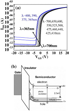
(a) Typical response to monochromatic light of transfer characteristic of annealed a-IGZO TFT. The photon flux was fixed at ∼1×10¹⁴ photons (cm-2 s-1). The blue dashed lines correspond to illumination above the band gap (>3.1 eV) and the black solid lines correspond to subgap illumination. (b) Model to explain NBL instability.
A similar photoresponse is also observed in steady-state photocurrent measurements of a-IGZO films [137], which show that the mobility-lifetime product decays slowly with the corresponding Urbach energies of ∼0.24 eV for unannealed a-IGZO and ∼0.16 eV for annealed a-IGZO. The photoresponse is reversible and very slow with a time constant exceeding thousands of seconds. This is attributed to the relaxation of metastable donor states with activation energies of 0.9–1.1 eV, and a similar model was proposed by Takechi et al [136].
An enhanced negative Vth shift is observed if a negative bias is applied with illumination (i.e. NBL stress) [138]. Lee et al reported that the NBL stability depends on the quality of the initial a-IGZO layers; i.e. although initial performance of high-quality and low-quality a-IGZO TFTs is similar, the latter are rapidly degraded by stress [139]. We found that low-quality films have a much higher deep-subgap DOS, although their Hall mobilities and TFT characteristics appear similar to those of high-quality films [4]. These results indicate that only the electrical characteristics themselves cannot be used as an indicator of film quality, and it is important to improve the film quality to as high as possible to produce stable a-IGZO TFTs.
Lee et al [140] proposed a hole-trap model to explain the NBL instability. In this model, photoexcitation occurs from the valence band to subgap electron traps; electrons are localized at the subgap traps and holes are transported to traps in a channel—gate insulator interface or a gate insulator. We consider a similar mechanism but with the Fermi level in the a-IGZO channels rather high in the band gap above 0.5 eV below CBM (i.e. ∼2.5 eV above VBM) for the usual electron density [5], and with a small subgap DOS near CBM as discussed in section 5.6; therefore, the excitation to electron traps cannot explain the photoresponse under the 2.3 eV subgap illumination (note that almost all the subgap states are fully occupied below the Fermi level). Therefore, we consider that the subgap photon excitation mostly occurs from the deep-subgap DOS to the conduction band. Lee et al [140] also pointed out that moisture enhances the NBL instability [140]. Sony reported that the use of a dc-sputtered AlOx passivation layer suppressed the photoresponse to a cold cathode fluorescent lamp [130]. For poly-ZnO TFTs, the Kyoto University and Kochi University of Technology groups reported that the photoleakage current originates from the large photoresponse in the source region [141].
TFT modeling
Many subgap DOS and mobility models and analytical models have been reported for a-IGZO TFTs; however, combined and unified models have not been established yet. Here, we simply list the references for device simulation models [98, 142, 143], DOS models based on C–V methods [99], combinations of C–V methods and device simulations [100–104, 106], mobility models [105, 144], subthreshold models based on the Meyer–Neldel rule [145, 146], temperature dependences [143, 147] and circuit design [148, 149].
Fundamental properties and physics of a-IGZO
Origin of large electron mobility in a-IGZO: pseudo-band structure
Hereafter, we discuss the fundamental physics and properties of AOSs. The first issue is why AOS TFTs have a good performance superior to that of a-Si:H TFTs, even though both AOSs and a-Si:H are amorphous. Before the report on transparent amorphous oxide conductors in 1995 [24–27], amorphous conductors were thought to have poor electronic conductivity because of hopping conduction in the disordered structure. This is the case for a-Si:H, where both electrons and holes migrate by hopping and not by band conduction, which is why the electron mobilities are as low as <1 cm2 V-1 s-1 (see section 5.4 and [87]). In contrast, the electron mobilities in AOSs easily exceed 10 cm2 V-1 s-1, and band conduction is observed, as evidenced by the clear Hall voltage signals and the degenerated temperature dependence of the Hall mobility [1, 144, 150]. This difference is explained by chemical bonding in [4]. The sp3 hybridized orbitals that form the carrier transport paths in Si are markedly distorted by disorder and form deep localized states. This results in the hopping conduction and the low drift mobilities in a-Si:H. In contrast, the electron paths in oxides of typical metals are formed mainly by s orbitals of the metal cations, and the overlaps between the wave functions of adjacent metal cations are not altered significantly by the disorder in AOSs, thus enabling band conduction and high mobilities.
This chemical bonding view is supported by first-principles DFT calculations. Figure 17 shows pseudo-band structures of a-InGaZnO4 and a-Si. Note that band theory is not applicable to non-periodic systems, but periodic calculations are still helpful to for understanding the stable atomic configurations and the nature of chemical bonds even for amorphous materials. In particular, the width of a band in such a (pseudo-)band structure reflects the local effective mass and transfer integrals [151, 152]. Figure 17(a) shows that the CBM band at ∼0.7 eV has a large dispersion with a bandwidth of ∼1 eV, similar to that of crystalline InGaZnO4 (c-IGZO) (the band effective masses are calculated as me∗=0.2 me for a-IGZO [153] and 0.18 me for c-IGZO [111]), indicating that the electrons in a-IGZO are delocalized.
Figure 17.
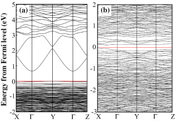
Pseudo-band structures of (a) a-InGaZnO4 and (b) a-Si.
Calculations for a-Si (performed for a Si64 unit cell using a similar procedure to that in [153]) show that all the bands have very small widths, much less than 0.5 eV, indicating the suppression of band conduction. The band dispersion in a-Si is markedly suppressed because of the strong spatial directivity of the sp3 hybridized orbitals.
Similar results were obtained for a-IGZO in the high-energy conduction band region above 3 eV and the valence band region. The former is formed mainly by the p orbitals of metal cations and the latter is formed by the p orbitals of oxygen ions, whereas the CBM band is mainly composed of the s orbitals of metal cations. These results support the chemical bonding considerations above. Note that the valence band dispersion is very small and that isolated bands are found (at –0.2–0 eV) in a-IGZO, indicating that holes are strongly localized.
Carrier transport mechanism
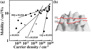
In–Ga–Zn–O exhibits unusual carrier transport properties as shown in figure 13(a). In particular, (i) its electron mobility increases with increasing free-electron density, (ii) the maximum Hall mobility is similar for crystalline InGaO3(ZnO)m [154] and a-IGZO. The reason for (ii) is explained in section 6.1: the band dispersions, i.e. the effective masses, are similar for c-IGZO and a-IGZO because their CBM bands are formed by the s orbitals. Behavior (i) is opposite that of single-crystalline semiconductors, in which the carrier mobility usually decreases with increasing carrier density because of scattering on the ionized donors or acceptors.
Behavior (i) is explained by a percolation conduction model [105, 144, 150, 154]. As illustrated in figure 13(b), a distribution of potential barriers is formed above CBM owing to the disordered structure. Electrons take shorter transport paths at high temperatures even if these paths have high potential barriers (path (i) in figure 13(b)). They take a longer path (ii) with lower barriers at lower temperatures because they do not have sufficient thermal energy to pass the high potential barriers. In this model, the distribution of the potential barrier heights is characterized by the center energy (φ0) and distribution width (σφ). The model reproduces the temperature (T) dependences of Hall measurements as shown in figures 18(a) and (b). The distributed potential barriers result in the deviation from simple thermal activation; i.e. the Arrhenius plot of conductivity (σ) shows nonlinear behavior in figure 18(b) and a better straight line is obtained in the log σ∼T-n (n∼ 1/4) plot. Such behavior is usually explained by Mott's variable-range hopping, but it cannot be applied to a-IGZO because this material exhibits clear Hall voltage signals.
Figure 18.
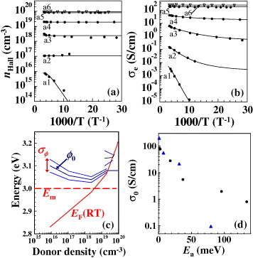
(a, b) Temperature dependences of (a) electron density and (b) conductivity measured using the Hall effect. The symbols show experimental data and the solid lines were calculated using the percolation conduction model. (c) Electronic structure in the conduction band of a-IGZO extracted from the data in (a, b). (d) Examination of the Meyer–Neldel rule. The circles show c-IGZO data and triangles correspond to a-IGZO.
At intermediate electron densities, a weak localization behavior is observed in which σ follows the relation σ(T)=σ0+ηTp/2+λT1/2. Here σ0, η and λ are constants and p reflects the carrier scattering mechanism. For example, p=1 corresponds to photon scattering [155–157]. This behavior can be explained by the percolation conduction model. Weak localization is also observed in amorphous In–O and In–Zn–O and is confirmed by the magnetic field response [158–161]. At lower electron densities, a Hall voltage anomaly appears in a-IGZO films at low temperatures (<120 K) as seen in the deviation of the calculated electron densities from the measured values (figure 18(a)).
Semiconductor statistics analysis of nHall(T) data yields donor levels at 100–150 meV for c-IGZO and at 110 meV below CBM for a-IGZO [105], and the percolation conduction model indicates that the potential barriers have an average height of 40–120 meV and a width of 20–30 meV as shown in figure 18(c).
It would also be interesting to examine the Meyer-Neldel (MN) rule [162], which is valid for many semiconductors including a-Si:H [163, 164]. Conventionally σ is expressed as σ=σ0 exp(-Ea/kBT), where σ0 is a prefactor and Ea is the activation energy. The MN rule indicates that ln σ0 and Ea are linearly related, i.e. σ0=σ00 exp(AEa),A >0, and this behavior in a-Si:H is related to the localized tail states [165]. The ln σ0–Ea plot is presented in figure 18(d), but both c-IGZO and a-IGZO exhibit negative values of A. This behavior is called the ‘anti-MN rule’ and is observed, for example, in hydrogenated microcrystalline silicon (μc-Si:H) [166]. A regular MN relation was reported for a-IGZO TFTs [145, 146] in a large Ea region that corresponds to a low VGS and a low carrier density (Ne). This changes to the anti-MN rule for low Ea<80 meV [146], which is consistent with the data in figure 18(d) and similar to the case of μc-Si:H.
Let us consider effective masses. The effective mass of a-IGZO (In:Ga:Zn=1:1:1) is estimated to be ∼0.34 me from free-carrier absorption in highly doped a-IGZO films [150]. This value is similar to that of c-IGZO (0.32 me) and is consistent with the chemical bonding view discussed in section 6.1. Medvedeva [167] reports that electron effective masses in multicomponent transparent oxides can be estimated from their chemical composition. Canon investigated AOSs in the In-X-O system (X=Al, Si, Ge, etc) with various compositions and found a clear relation between the estimated effective mass and μsat [168, 169].
As described above, it is easy to obtain a Hall mobility above 10 cm2 V-1 s-1 for a-IGZO (In:Ga:Zn=1:1:1), but larger mobilities are obtained for In-rich and Ga-poor compositions [170]. Especially, Zn-doped amorphous indium oxide with ∼10 wt% ZnO, which is called IZO, exhibits very high mobilities of up to 54 cm2 V-1 s-1 [171]. The mobility of a-IZO increases with increasing Ne for Ne<1020 cm-3 and decreases at higher Ne. Such a decrease at high Ne is not observed for a-IGZO, while the increase in mobility with Ne extends to a wider range of Ne. It should be noted that the decrease in μ in the high Ne range is attributed not to conventional ionized impurity scattering but to other defects which are responsible for the `gray’ optical absorption in highly doped a-IZO.
In figure 19, the optical band gap is plotted against Ne2/3 for a-IGZO [5] and a-IZO [171]. The figure shows that the optical band gap increases with increasing Ne, which is due to the band-filling effect, that is, the Burstein–Moss shift ΔEgBM
The DOS effective mass mde is obtained from the slope of this plot to be ∼0.56 me for a-IZO. For a-IGZO, the ΔEgBM−Ne2/3 plot does not follow a straight line, which might be due to the nonparabolic bands or the band-narrowing effect [5].
Figure 19.
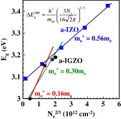
Effects of band filling in a-IGZO [5] and a-IZO [165]; the effective masses m*e were calculated using the straight lines in the figure.
Optical properties
Band gap values of AOSs are usually estimated from a Tauc plot [172], which has the form αE=[B(E−Eg)]r (α is the absorption coefficient, E is the photon energy, and B and r are constants). Assuming parabolic bands and the vanishing of the k-selection rule for optical transitions, which is valid for a crystal, r=2 is usually employed in the Tauc plot. The estimated band gap (Tauc gap) is ∼3.2 eV for high-quality a-IGZO films (In:Ga:Zn=1:1:1) and tends to decrease to ∼3.0 eV for poor-quality films. It has also been reported that the Tauc-Lorentz model [173, 174] closely fits to the optical spectra of a-IGZO and c-IGZO [110, 175]. As discussed in relation to the deep subgap DOS and the NBL instability in sections 5.6–5.8, subgap optical absorption is important for the TFT stability [86]. It was found that optical absorption spectra just below the band gap follow the Urbach law with an Urbach energy of ∼150 meV [109].
Optical spectra also provide information about the subgap DOS. The a-IGZO films in figure 20 have band gaps of 3.0–3.2 eV, but there is observable optical absorption in the photon energy range from 2.0 eV to the band gap values (figures 20(b) and (c)). The widths of these subgap optical absorption features correspond well to the deep-subgap DOS above VBM observed by HX-PES in figure 14(b), and they are considered to have the same origin.
Figure 20.
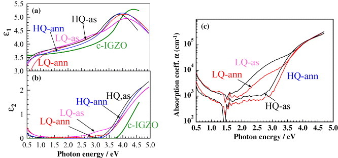
Optical spectra of various a-IGZO. HQ, LQ, as and ann denote high-quality, low-quality, as-deposited and annealed films, respectively (see [107]). (a) Real and (b) imaginary parts of dielectric function. (c) Optical absorption spectrum. [110].
Structure analysis
It is difficult to deduce the atomic structure of an amorphous material. The structure of AOSs was studied by grazing-incidence x-ray scattering (GIXS) and x-ray absorption fine structure (XAFS) combined with molecular dynamics (MD), reverse Monte–Carlo simulations and DFT calculations. Utsuno et al have reported the structures of a-In2O3 [176] and a-IZO [177] and found the number of edge-sharing network structures decreases and the number of In–Zn corner-sharing structures increases with increasing Zn content. We constructed a-IGZO models from MD/DFT calculations based on the coordination structure obtained from XAFS, which showed that the coordination numbers around the cations are similar but slightly smaller than those in the corresponding crystals [5, 153]. Cho et al reported that the coordination structure of the Zn ions is distorted; they suggested that holes are localized on the Zn atoms [178] as on the basis of a DFT result for crystalline ZnO [179]. This view of the localized holes is consistent with DFT pseudo-band calculations for a-IGZO [110, 111], but the verification of hole states is very difficult for a-IGZO because it is a wide-band-gap n-type semiconductor with almost no holes, unless illuminated.
The common conclusions of these studies are (i) the nearest-neighbor bond distances are similar in AOSs and the corresponding crystals, (ii) the coordination numbers of cations are similar or slightly smaller than those in the corresponding crystals (e.g. 4.5–6 for In, 4.3–5 for Ga-O and 4.6–5 for Zn-O), (iii) InOn polyhedra tend to form edge-sharing networks. The In-In distances are different between crystalline In2O3, c-IGZO and a-IGZO because of different angles in the connecting InOn polyhedra.
Electronic structures, doping, impurities and defects
There have been several reports on theoretical calculations of the electronic structure and defects in c-IGZO [181–186] and a-IGZO [109–111, 153, 185, 187]. The pseudo-band structure is shown in figure 17(b) and the projected DOS is shown in figure 21, which corresponds to the peak in the valence band of HX-PES in figure 14(b). The calculated energy levels are underestimated because DFT provides energy levels as types of chemical potentials [188], which are smaller than ionization potentials. In addition, it is known that the incorporation of Coulomb repulsion is important for Zn 3d electrons [179] because omission of it raises the energy levels of Zn 3d and results in an overestimation of the Zn 3d–O 2p interaction and the VBM dispersion and in the further underestimation of the band gap.
Figure 21.
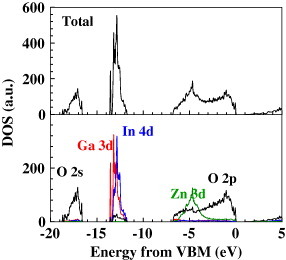
Total and projected DOSs of a-IGZO calculated using a (InGaZnO4)17 cell.
DFT calculations have provided the following information. Different structures with different densities from 5.8 to 6.1 g cm-3 can be stable ([153] and unpublished data). The film density measured by grazing-incidence x-ray reflectivity (GIXRR) was ∼6.1 g cm-3. This value is ∼4% smaller than that of crystalline InGaZnO4 (x-ray density, 6.379 g cm-3) but is in good agreement with the DFT results.
Oxygen deficiency in a-IGZO results in both deep, fully occupied states and shallow donor states in the band gap, which depend on the local structure of the oxygen defect [109]. A large open space in the structure traps electrons and forms a deep level similar to the deep-subgap DOS observed by HX-PES. It simultaneously forms a shallow unoccupied trap because the coherence of the CBM band is broken by the vacancy site [110]. If such a large open space is not formed in oxygen-deficient a-IGZO, then shallow donor states are formed that contributes to the enhancement of electronic conductivity.
Figure 22 shows several oxygen deficiency structures. If an oxygen vacancy site is coordinated by a small number of cations (a) or if it is adjacent to a large open space (b), then deep traps and shallow traps are formed, whereas if an oxygen vacancy site is coordinated by a large number of cations with dense edge-sharing networks, then a shallow donor state is created. Whereas this tendency does not always hold, numerous calculations have confirmed it to be a general trend. This implies that the elimination of open spaces should be effective for making high-quality a-IGZO with fewer defects. Jeong et al came to a similar conclusion. They reported a variation in the a-IGZO density from 5.50 to 6.27 g cm-3 for different deposition conditions; denser films had smaller S values and thus fewer defects [189]. We speculate that such an open space may also be related to the metastable donor states observed by steady-state photoconductivity measurements [137].
Figure 22.
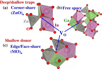
Local coordination structures of some oxygen deficiencies. The small red spheres represent O ions, green spheres are Ga, gray spheres are Zn and pink spheres are In atoms. The red spheres indicated by the arrows are oxygen vacancy sites. ‘Corner-share’, ‘Free space’ and ‘Edge/Face-share’ describe the structures around the oxygen vacancy sites.
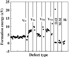
DFT calculations provide the defect formation energies summarized in figure 23. The minimum formation energies are 2.0 eV for an oxygen vacancy (VO), 6.1 eV for an indium vacancy (VIn), 4.0 eV for a zinc vacancy (VZn) and 5.1 eV for a gallium vacancy (VGa) at the reduction limit. Takechi et al estimated the defect formation energy from the temperature dependences of TFT characteristics. They obtained a value of 1.05 eV, which corresponds to an activation energy of 0.35 eV [147]. This value is, however, much smaller than the high-temperature (<300 °C) conductivity activation energies of 0.65–1.5 eV [118], which correspond to the defect formation energies of 2–4.5 eV and agree well with the DFT results. Figure 23 also provides the formation energies of other defects such as O–O and metal–metal (M–M) linkages, as well as that of excess hydrogen at a bond center (Hi) at the reduction limit, showing that these defects can be easily formed in a-IGZO.
Figure 23.
Formation energies for various defects in a-IGZO calculated by DFT.
Regarding hydrogen doping, DFT calculations showed that the incorporation of a hydrogen atom into a-IGZO always results in a shallow donor state [110, 111], but the incorporation of a H2 molecule would not change the chemical bonds and electronic structure (unpublished).
It has been reported that a-IGZO films deposited by sputtering contain hydrogen with a concentration above 3×1020 cm-3 which further increases to 2×1021 cm-3 with increasing H2O pressure during the deposition; however TFTs using these a-IGZO channels exhibit a positive Vth [190]. On the other hand, we observed that the low-temperature (∼200 °C) annealing of a-IGZO films in a diluted H2 gas increases the carrier density to ∼1020 cm-3. These results appear contradictory but can be explained using the DFT results and the electronic structure in figure 10(b). DFT calculations for H-incorporated a-IGZO suggest that hydrogen atoms, but not molecules, form –OH bonds and shallow donors. In addition, even if the incorporated hydrogen creates donors, they might be compensated by the deep traps as observed by HX-PES. This is an important issue to be clarified in the near future.
References
- Nomura K, Ohta H, Takagi A, Kamiya T, Hirano M. and Hosono H. Nature. 2004;432:488. doi: 10.1038/nature03090. [DOI] [PubMed] [Google Scholar]
- Kim H D, Park J-S, Mo Y G and Kim S S. 2009. 9th Int. Meeting on Information Display (12–16 October 2009, Seoul, Korea) 3-1 [Google Scholar]
- Hung M-C, Lin W-T, Chang J J, Chen P-L, Wu C-Y, Lin C-J, Chiu H-L, Huang C-Y and Kao Y-C. 2010. Int. Workshop on Transparent Amorphous Oxide Semiconductors 2010 (25–26 January 2010, Tokyo, Japan) [Google Scholar]
- Kamiya T. and Hosono H. NPG Asia Mater. 2010;2:1522. [Google Scholar]
- Kamiya T, Nomura K. and Hosono H. J. Disp. Technol. 2009;5:273. doi: 10.1109/JDT.2009.2021582. [DOI] [Google Scholar]
- Special Issue on Transparent Electronics 2009 J. Disp. Technol. Issue 12 [Google Scholar]
- Hahn E E. J. Appl. Phys. 1951;22:855. doi: 10.1063/1.1700063. [DOI] [Google Scholar]
- Tsukazaki A.et al2005Nat. Mater. 442. 10.1038/nmat1284 [DOI] [Google Scholar]
- Ohta H, Kawamura K, Orita M, Hirano M, Sarukura N. an an an and Hosono H. Appl. Phys. Lett. 2000;77:475. doi: 10.1063/1.127015. [DOI] [Google Scholar]
- Look D C, Claflin B, Alivov Y I and Park S J. 2004. Phys. Status Solidi a 201 2203 10.1002/pssa.200404803 [DOI] [Google Scholar]
- Tsukazaki A, Ohtomo A. and Kawasaki M. Appl. Phys. Lett. 2006;88:152106. doi: 10.1063/1.2193727. [DOI] [Google Scholar]
- Ohtomo A. and Hwang H Y. Nature. 2004;427:423. doi: 10.1038/nature02308. [DOI] [PubMed] [Google Scholar]
- Kamiya T. and Kawasaki M. MRS Bull. 2008;33:1061. [Google Scholar]
- Boesen G F. and Jacobs J E. Proc. IEEE. 1968;56:2094. doi: 10.1109/PROC.1968.6813. [DOI] [Google Scholar]
- Weimer P K. Proc. IRE. 1962;50:1462. doi: 10.1109/JRPROC.1962.288190. [DOI] [Google Scholar]
- Klasens H A. and Koelmans H. Solid-State Electron. 1964;7:701. doi: 10.1016/0038-1101(64)90057-7. [DOI] [Google Scholar]
- Aoki A. and Sakakura H. Japan. J. Appl. Phys. 1970;9:582. doi: 10.1143/JJAP.9.582. [DOI] [Google Scholar]
- Furuta M, Matsuda T, Hiramatsu T, Furuta H, Hirao T, Yoshida M, Hokari H, Ishii H an and Kakegawa M. 2006. Proc. 13th Int. Display Workshop p 677 [Google Scholar]
- Hirao T, Furuta M, Furuta H, Matsuda T, Hiramatsu T, Hokari H, Yoshida M, Ishii H. and Kakegawa M. J. Soc. Inf. Disp. 2007;15:17. doi: 10.1889/1.2451545. [DOI] [Google Scholar]
- Park S-H K, Hwang C-S, Lee J-I, Chung S M, Yang Y S, Do L-M and Chu H Y. 2006. Digest of SID2006 (4–9 June 2006, San Francisco, USA) p 25 [Google Scholar]
- Park S-H K, Hwang C-S, Ryu M, Yang S, Byun C, Shin J, Lee J-I, Lee K, Oh M S. and Im S. Adv. Mater. 2009;21:678. doi: 10.1002/adma.200801470. [DOI] [Google Scholar]
- Hebard A F. Appl. Phys. Lett. 1982;41:1130. doi: 10.1063/1.93408. [DOI] [Google Scholar]
- Bellingham J R. J. Physique. 1990;2:6207. [Google Scholar]
- Hosono H, Kikuchi N, Ueda N. an an and Kawazoe H. J. Non-Cryst. Solids. 1996;198–200:165. doi: 10.1016/0022-3093(96)80019-6. [DOI] [Google Scholar]
- Yasukawa M, Hosono H, Ueda N. and Kawazoe H. Japan. J. Appl. Phys. 1995;34:L281. doi: 10.1143/JJAP.34.L281. [DOI] [Google Scholar]
- Hosono H, Kikuchi N, Ueda N, Kawazoe H. and Shimidzu K. Appl. Phys. Lett. 1995;67:2663. doi: 10.1063/1.114329. [DOI] [Google Scholar]
- Hosono H, Yamashita Y, Ueda N, Kawazoe H. and Shimidzu K. Appl. Phys. Lett. 1996;68:661. doi: 10.1063/1.116501. [DOI] [Google Scholar]
- Hosono H, Maeda H, Kameshima Y. and Kawazoe H. J. Non-Cryst. Solids. 1998;227–230:804. doi: 10.1016/S0022-3093(98)00169-0. [DOI] [Google Scholar]
- Orita M, Ohta H, Hirano M, Narushima S and Hosono H. 2001. Phil. Mag. B 81 501 [Google Scholar]
- Nomura K, Ohta H, Ueda K, Kamiya T, Hirano M. and Hosono H. Science. 2003;300:1269. doi: 10.1126/science.1083212. [DOI] [PubMed] [Google Scholar]
- Staebler D L. and Wronski C R. Appl. Phys. Lett. 1977;31:292. doi: 10.1063/1.89674. [DOI] [Google Scholar]
- Street R A. Technology and Applications of Amorphous Silicon. Berlin: Springer; 2000. [Google Scholar]
- Jahinuzzaman S M, Sultana A, Sakariya K, Servati P. an and Nathan A. Appl. Phys. Lett. 2005;87:023502. doi: 10.1063/1.1993766. [DOI] [Google Scholar]
- Higashi S, Abe D, Hiroshima Y, Miyashita K, Kawamura T, Inoue S. and Shimoda T. Japan. J. Appl. Phys. 2002;41:3646. doi: 10.1143/JJAP.41.3646. [DOI] [Google Scholar]
- Kamiya T, Durrani Z A K, Ahmed H, Sameshima T, Furuta Y, Mizuta H and Lloyd N. 2003. J. Vac. Sci. Technol. B 21 1000 10.1116/1.1570849 [DOI] [Google Scholar]
- Jeong J K, Mo Y-G, Ryu M K and Yang S. 2010. Int. Workshop on Transparent Amorphous Oxide Semiconductors 2010 (25–26 January 2010, Tokyo, Japan) [Google Scholar]
- Kwon J Y, Jung J S, Son K S, Kim T S, Ryu M K, Park K B, Park Y S, Lee S Y and Kim J M. 2008. Digest of 15th Int. Workshop on Active-Matrix Flatpanel Displays and Devices 287 (2–4 July 2010, Tokyo, Japan) [Google Scholar]
- Matsueda Y. 2010. Digest of Int. Transistor Conf. 2010 (28–29 January 2010, Hyogo, Japan) p 314 [Google Scholar]
- Song I, Kim S, Yin H, Kim C J, Park J, Kim S, Choi H S, Lee E. an and Park Y. IEEE Electron Device Lett. 2008;29:549. doi: 10.1109/LED.2008.920965. [DOI] [Google Scholar]
- Ito M, Kon M, Okubo T, Ishizaki M and Sekine N. 2005. Proc. Int. Display Workshop/Asia Display 2005 (6–9 December 2005, Takamatsu, Japan) p 845 [Google Scholar]
- Lee H N, Kyung J W, Kang S K, Kim D Y, Sung M C, Kim S J, Kim C N, Kim H G and Kim S T. 2006. Proc. Int. Display Workshop 2006 (6–8 December 2006, Otsu, Japan) p 663 [Google Scholar]
- Jeong J K. et al 2007. 7th Int. Meeting on Information Display (27–31 August 2007, Daegue, Korea) 9-4 [Google Scholar]
- Kwon J Y. et al 2007. 7th Int. Meeting on Information Display (27–31 August 2007, Daegue, Korea) 9-3 [Google Scholar]
- Jeong J K. et al 2008. Digest of SID2008 (18–23 May 2010, Los Angeles, USA) p 1 [Google Scholar]
- Jeong J K.et al2009J. SID 1795 [Google Scholar]
- Lee J-H. et al 2008. Digest of SID2008 (18–23 May 2010, Los Angeles, USA) p 625 [Google Scholar]
- Kawamura T, Uchiyama H, Saito S, Wakana H, Mine T, Hatano M, Torii K an an an an an and Onai T. 2008. Digest of International Electron Devices Meeting 2008 (15–17 December 2008, San Francisco, USA) [Google Scholar]
- Lu H-H, Ting H-C, Shih T-H, Chen C-Y, Chuang C-S and Lin Y. 2010. Digest of SID2010 (23–28 May 2010, Seattle, USA) p 1136 [Google Scholar]
- Kim H D, Park J-S, Mo Y G and Kim S S. 2009. Digest of Int. Meeting on Information Display 2009 (12–16 October, Seoul, Korea) p 35 [Google Scholar]
- Osada T, Akimoto K, Sato T, Ikeda M, Tsubuku M, Sakata J, Koyama J, Serikawa T and Yamazaki S. 2009. Digest of 16th Int. Workshop on Active-Matrix Flatpanel Displays and Devices (1–3 July 2009, Nara, Japan) 3-3 [Google Scholar]
- Osada T, Akimoto K, Sato T, Ikeda M, Tsubuku M, Sakata J, Koyama J, Serikawa T and Yamazaki S. 2009. Digest of SID2009 (31 May–5 June 2009, San Antonio, USA) p 284 [Google Scholar]
- Osada T, Akimoto K, Sato T, Ikeda M, Tsubuku M, Sakata J, Koyama J, Serikawa T and Yamazaki S. 2009. Digest of SID2009 (31 May–5 June 2009, San Antonio, USA) p 184 [Google Scholar]
- Ohta Y. et al 2009. Digest of Int. Display Workshop 2009 (9–11 December 2009, Miyazaki, Japan) AMD7-4 [Google Scholar]
- Seo H-S, Bae J-U, Kim D-W, Ryoo C I, Kang I K, Min S-Y, Kim Y-Y, Han J-S, Kim C-D an and Hwang Y. 2010. Int. Workshop on Transparent Amorphous Oxide Semiconductors 2010 (25–26 January 2010, Tokyo, Japan) [Google Scholar]
- Ito M, Miyazaki C, Ikeda N and Kokubo Y. 2009. 16th Int. Workshop on Active-Matrix Flatpanel Displays and Devices (1–3 July 2009, Nara, Japan) S-2 [Google Scholar]
- Sung M-C, Lee H-N, Kim C N, Kang S K, Kim D Y, Kim S-J, Kim S K, Kim S-K, Kim H-G and Kim S-t. 2007. 7th Int. Meeting Information Display (27–31 August 2007, Daegue, Korea) 9–1 [Google Scholar]
- Park J-S, Kim T, Stryakhilev D, Lee J-S, An S-G, Pyo Y-S, Lee D-B, Mo Y G, Jin D-U. and Chung H K. Appl. Phys. Lett. 2009;95:013503. doi: 10.1063/1.3159832. [DOI] [Google Scholar]
- Arihara K, Kano M, Motai K, Naitou Y, Kadowaki M, Nakajima H, Tsuboi T, Kato C, Kishimoto Y and Maeda H. 2009. Digest of Int. Display Workshop 2009 (9–11 December 2009, Miyazaki, Japan) FLX4-3 [Google Scholar]
- Ito M, Kon M, Miyazaki C, Ikeda N, Ishizaki M, Ugajin Y. and Sekine N. IEICE Trans. Electron. 2007;E90-C:2105. doi: 10.1093/ietele/e90-c.11.2105. [DOI] [Google Scholar]
- Jeong J K. et al 2007. 47th Int. Meeting on Information Display (27–31 August 2007, Daegue, Korea) 9-4 [Google Scholar]
- Song Y W, Hwang K H, Yoon S G, Ha J H, Kim K N, Lee J H an and Kim S C. 2010. Digest of SID2010 (23–28 May 2010, Seattle, USA) p 144 [Google Scholar]
- Hsieh H-H. et al 2010. Digest of SID2010 (23–28 May 2010, Seattle, USA) p 140 [Google Scholar]
- Yin H, Kim S, Kim C J, Song I, Park J, Kim S. an and Park Y. Appl. Phys. Lett. 2008;93:172109. doi: 10.1063/1.3012386. [DOI] [Google Scholar]
- Chen M-C, Chang T-C, Huang S-Y, Chen S-C, Hu C-W, Tsai C-T. and Sze S M. Electrochem. Solid-State Lett. 2010;13:H191. doi: 10.1149/1.3360181. [DOI] [Google Scholar]
- Seo J W, Park J-W, Lim K S, Kang S J, Hong Y H, Yang J H, Fang L, Sung G Y. and Kim H-K. Appl. Phys. Lett. 2009;95:133508. doi: 10.1063/1.3213390. [DOI] [Google Scholar]
- Yabuta H, Sano M, Abe K, Aiba T, Den T, Kumomi H, Nomura K, Kamiya T. and Hosono H. Appl. Phys. Lett. 2006;89:112123. doi: 10.1063/1.2353811. [DOI] [Google Scholar]
- Sakata J. et al 2009. Digest of 16th Int. Workshop Active-Matrix Flatpanel Displays and Devices (1–3 July 2009, Nara, Japan) AMD4/OLED4-2 [Google Scholar]
- Kurata T, Yanagi Y, Isobe T, Akamatsu Y, Arai M, Kiyota J, Ishibashi S an an and Saito K. 2010. 57th Spring Meeting of Japanese Society for Applied Physics (17–20 March 2010, Kanagawa, Japan) 17a-TL5 [Google Scholar]
- Ukai Y. 2007. Thin-Film Transistors (Hakumaku Transistor Gijutsu no Subete) (in Japanese) [Google Scholar]
- Hung C-C, Lin W-T, Tu C-H, Kao Y-C, Wu C-Y, Chang J-J an and Chen P-L. 2010. Digest of 17th Int. Workshop on Active-Matrix Flatpanel Displays and Devices (5–7 July 2010, Tokyo, Japan) pp 3–4 [Google Scholar]
- Mo Y G, Kim M, Kang C K, Jeong J H, Park Y S, Choi C G, Kim H D and Kim S S. 2010. Digest of SID 2010 (23–28 May 2010, Seattle, USA) p 1037 [Google Scholar]
- Yun P S and Koike J. 2010. 57th Spring Meeting of Japanese Society for Applied Physics (17–20 March 2010, Kanagawa, Japan) 17a-TL4 [Google Scholar]
- Ito M, Miyazaki C, Ikeda N, Ishizaki M and Ugajin Y. 2010. Int. Workshop on Transparent Amorphous Oxide Semiconductors 2010 (25–26 January 2010, Tokyo, Japan) [Google Scholar]
- Lee D-H, Chang Y-J, Herman G S. and Chang C-H. Adv. Mater. 2007;19:843. doi: 10.1002/adma.200600961. [DOI] [Google Scholar]
- Lim J H, Shim J H, Choi J H, Joo J, Park K, Jeon H, Moon M R, Jung D, Kim H. and Lee H-J. Appl. Phys. Lett. 2009;95:012108. doi: 10.1063/1.3157265. [DOI] [Google Scholar]
- Ryu M K, Park K, Seon J-B, Park J, Kee I, Lee Y and Lee S Y. 2009. Digest of SID2009 (31 May–5 June 2009, San Antonio, USA) 15.3 [Google Scholar]
- Seon J-B, Ryu M-K, Park K-B, Kee I, Lee Y, Koo B-W and Lee S Y. 2009. Digest of Int. Display Workshop 2009 (9–11 December 2009, Miyazaki, Japan) AMD8-2 [Google Scholar]
- Lai Y-C. et al 2009. Digest of Int. Display Workshop 2009 (9–11 December 2009, Miyazaki, Japan) AMD8-3 [Google Scholar]
- Lim J H, Shim J H, Choi J H, Joo J, Park K, Jeon H, Moon M R, Jung D, Kim H. an and Lee H-J. Appl. Phys. Lett. 2009;95:012108. doi: 10.1063/1.3157265. [DOI] [Google Scholar]
- Kim M, Han J, Lee H J, Ahn T K, Shin H S, Park J-S, Jeong J K, Mo Y-G. and Kim H D. Appl. Phys. Lett. 2007;90:212114. doi: 10.1063/1.2742790. [DOI] [Google Scholar]
- Kagan C R, and Andry P, , editors. Thin-Film transistors. New York: Marcel Dekker; 2003. [Google Scholar]
- Sze S Z. Physics of Semiconductor Devices. 2nd edn. New York: Wiley; 1981. [Google Scholar]
- Street R A. Technology and Applications of Amorphous Silicon. Berlin: Springer; 2000. [Google Scholar]
- Martin S, Chiang C-S, Nahm J-Y, Li T, Kanicki J. an an and Ugai Y. Japan. J. Appl. Phys. 2001;40:530. doi: 10.1143/JJAP.40.530. [DOI] [Google Scholar]
- Nomura K, Kamiya T and Hosono H. 2010. J. SID at press [Google Scholar]
- Fritzsche H and Chen K-J. 1983. Phys. Rev. B 28 4900 10.1103/PhysRevB.28.4900 [DOI] [Google Scholar]
- Chen C-W, Chang T-C, Liu P-T, Lu H-Y, Wang K-C, Huang C-S, Ling C-C. and Yuen T. IEEE Electron Device Lett. 2005;26:731. doi: 10.1109/LED.2005.855405. [DOI] [Google Scholar]
- Takechi K, Nakata M, Eguchi T, Yamaguchi H. and Kaneko S. Japan. J. Appl. Phys. 2009;48:081606. doi: 10.1143/JJAP.48.081606. [DOI] [Google Scholar]
- Reeves G K. and Harrisson H B. IEEE Electron Device Lett. 1982;3:111. doi: 10.1109/EDL.1982.25502. [DOI] [Google Scholar]
- Shimura Y, Nomura K, Yanagi H, Kamiya T, Hirano M. and Hosono H. Thin Solid Films. 2008;516:5899. doi: 10.1016/j.tsf.2007.10.051. [DOI] [Google Scholar]
- Park J-S, Jeong J K, Mo Y-G. and Kim H D. Appl. Phys. Lett. 2007;90:262106. doi: 10.1063/1.2753107. [DOI] [Google Scholar]
- Sato A, Abe K, Hayashi R, Kumomi H, Nomura K, Kamiya T, Hirano M. and Hosono H. Appl. Phys. Lett. 2009;94:133502. doi: 10.1063/1.3112566. [DOI] [Google Scholar]
- Ahn B D, Shin H S, Kim H J, Park J-S. and Jeong J K. Appl. Phys. Lett. 2008;93:203506. doi: 10.1063/1.3028340. [DOI] [Google Scholar]
- Park J.et al2008Appl. Phys. Lett. 93053501. 10.1063/1.2966145 [DOI] [Google Scholar]
- Wu C-H, Hsieh H-H, Chien C-W. an and Wu C-C. J. Disp. Technol. 2009;5:515. doi: 10.1109/JDT.2009.2026189. [DOI] [Google Scholar]
- Kim S, Park J, Kim C, Song I, Kim S, Park S, Yin H, Lee H-I, Lee E. and Park Y. IEEE Electron Device Lett. 2009;30:374. doi: 10.1109/LED.2009.2014181. [DOI] [Google Scholar]
- Hsieh H-H, Kamiya T, Nomura K, Hosono H. and Wu C-C. Appl. Phys. Lett. 2008;92:133503. doi: 10.1063/1.2857463. [DOI] [Google Scholar]
- Kimura M, Nakanishi T, Nomura K, Kamiya T. and Hosono H. Appl. Phys. Lett. 2008;92:133512. doi: 10.1063/1.2904704. [DOI] [Google Scholar]
- Lee S, Park S, Kim S, Jeon Y, Jeon K, Park J-H, Park J, Song I, Kim C J, Park Y, Kim D M. and Kim D H. IEEE Electron Device Lett. 2010;31:231. doi: 10.1109/LED.2009.2039634. [DOI] [Google Scholar]
- Jeon K.et al2008Appl. Phys. Lett. 93182102. 10.1063/1.3013842 [DOI] [Google Scholar]
- Park J-H.et al2008IEEE Electron Device Lett. 291292. 10.1109/LED.2008.2006415 [DOI] [Google Scholar]
- Park J-H.et al2009IEEE Electron Device Lett. 301069. 10.1109/LED.2009.2028042 [DOI] [Google Scholar]
- Park J-H.et al2010J. Electrochem. Soc. 157H272. 10.1149/1.3273203 [DOI] [Google Scholar]
- Kamiya T, Nomura K. an an an an and Hosono H. Disp. Technol. 2009;5:462. doi: 10.1109/JDT.2009.2022064. [DOI] [Google Scholar]
- Kimura M, Kamiya T, Nakanishi T, Nomura K. and Hosono H. Appl. Phys. Lett. 2010;96:262105. doi: 10.1063/1.3455072. [DOI] [Google Scholar]
- Nomura K, Kamiya T, Yanagi H, Ikenaga E, Yang K, Kobayashi K, Hirano M. and Hosono H. Appl. Phys. Lett. 2008;92:202117. doi: 10.1063/1.2927306. [DOI] [Google Scholar]
- Ohsawa T.et al2009Appl. Phys. Lett. 94042104. 10.1063/1.3075578 [DOI] [Google Scholar]
- Kamiya T, Nomura K, Hirano M an and Hosono H. 2008. Phys. Status Solidi c 5 3098 10.1002/pssc.200779300 [DOI] [Google Scholar]
- Kamiya T, Nomura K and Hosono H. 2009. Phys. Status Solidi a 206 860 10.1002/pssa.200881303 [DOI] [Google Scholar]
- Kamiya T, Nomura K and Hosono H. 2010. Phys. Status Solidi a 207 1698 10.1002/pssa.200983772 [DOI] [Google Scholar]
- Kamiya T, Tajima K, Nomura K, Yanagi H and Hosono H. 2008. Phys. Status Solidi a 205 1929 10.1002/pssa.200778850 [DOI] [Google Scholar]
- Ip K, Thaler G T, Yang H, Han S Y, Li Y, Norton D P, Pearton S J, Jang S. and Ren F. J. Cryst. Growth. 2006;287:149. doi: 10.1016/j.jcrysgro.2005.10.059. [DOI] [Google Scholar]
- Ozgur U, Alivov Y I, Liu C, Teke A, Reshchikov M, Dogan S, Avrutin V, Cho S-J. and Morkoc H. J. Appl. Phys. 2005;98:041301. doi: 10.1063/1.1992666. [DOI] [Google Scholar]
- Mosbacker H L, Strzhemechny Y M, White B D, Smith P E, Look D C, Reynolds D C. and Litton C W. Appl. Phys. Lett. 2005;87:012102. doi: 10.1063/1.1984089. [DOI] [Google Scholar]
- Nomura K, Kamiya T and Hosono H , to be submitted [Google Scholar]
- Shibuya T, Yoshinaka M, Shimane Y, Utsuno F, Yano K, Inoue K, Ikenaga E, Kim J J, Ueda S, Obata M. and Kobayashi K. Thin Solid Films. 2010;518:3008. doi: 10.1016/j.tsf.2009.09.170. [DOI] [Google Scholar]
- Nomura K, Kamiya T, Ohta H, Hirano M. and Hosono H. Appl. Phys. Lett. 2008;93:192107. doi: 10.1063/1.3020714. [DOI] [Google Scholar]
- Nomura K, Kamiya T, Hirano M. and Hosono H. Appl. Phys. Lett. 2009;95:013502. doi: 10.1063/1.3159831. [DOI] [Google Scholar]
- Tober E D, Kanicki J. and Crowder M S. Appl. Phys. Lett. 1991;59:1723. doi: 10.1063/1.106230. [DOI] [Google Scholar]
- Lee J-M, Cho I-T, Lee J-H. and Kwon H-I. Appl. Phys. Lett. 2008;93:093504. doi: 10.1063/1.2977865. [DOI] [Google Scholar]
- Suresh A. and Mutha J F. Appl. Phys. Lett. 2008;92:033502. doi: 10.1063/1.2824758. [DOI] [Google Scholar]
- Kang D, Lim H, Kim C, Song I, Park J, Park Y. and Chung J. Appl. Phys. Lett. 2007;90:192101. doi: 10.1063/1.2723543. [DOI] [Google Scholar]
- Park J-S, Jeong J K, Chung H-J, Mo Y-G. and Kim H D. Appl. Phys. Lett. 2008;92:072104. doi: 10.1063/1.2838380. [DOI] [Google Scholar]
- Jeong J K, Yang H W, Jeong J H, Mo Y-G. and Kim H D. Appl. Phys. Lett. 2008;93:123508. doi: 10.1063/1.2990657. [DOI] [Google Scholar]
- Ryu M K. et al 2009. Digest of Int. Meeting on Information Display 2009 (12–16 October Seoul, Korea) 26-4 [Google Scholar]
- Jeong J K, Yang S, Cho D-H, Park S-H K, Hwang C-S. an and Cho K I. Appl. Phys. Lett. 2009;95:123505. doi: 10.1063/1.3236694. [DOI] [Google Scholar]
- Jeong B-S. et al 2009. Digest of Int. Meeting on Information Display 2009 (12–16 October, Seoul, Korea) p 1040 [Google Scholar]
- Ryu M K. et al 2009. Digest of Int. Meeting on Information Display 2009 (12–16 October, Seoul, Korea) p 330 [Google Scholar]
- Arai T, Morosawa N, Tokunaga K, Terai Y, Fukumoto E, Fujimori T, Nakayama T, Yamaguchi T an an and Sasaoka T. 2010. Digest of SID2010 (23–28 May 2010, Seattle, USA) p 1033 [Google Scholar]
- Seo H-S, Bae J-U, Kim D-H, Park Y, Kim C-D, Kang I B, Chung I-J, Choi J-H. and Myoung J-M. Electrochem. Solid State Lett. 2009;12:H348. doi: 10.1149/1.3168522. [DOI] [Google Scholar]
- Nomura K, Kamiya T, Kikuchi Y, Hirano M. and Hosono H. Thin Solid Films. 2010;518:3012. doi: 10.1016/j.tsf.2009.09.193. [DOI] [Google Scholar]
- Fujii M, Uraoka Y, Fuyuki T, Jung J S. and Kwon J Y. Japan. J. Appl. Phys. 2009;48:04C091. doi: 10.1143/JJAP.48.04C091. [DOI] [Google Scholar]
- Görrn P, Lehnhardt M, Riedl T. and Kowalsky W. Appl. Phys. Lett. 2007;91:193504. doi: 10.1063/1.2806934. [DOI] [PubMed] [Google Scholar]
- Fung T-C, Chuang C-S, Nomura K, Shieh H-P D, Hosono H. and Kanicki J. J. Inf. Disp. 2008;9:21. [Google Scholar]
- Takechi K, Nakata M, Eguchi T, Yamaguchi H. and Kaneko S. Japan. J. Appl. Phys. 2009;48:010203. doi: 10.1143/JJAP.48.010203. [DOI] [Google Scholar]
- Lee D H, Kawamura K, Nomura K, Kamiya T. and Hosono H. Electrochem. Solid State Lett. 2010;13:H324. doi: 10.1149/1.3460302. [DOI] [Google Scholar]
- Ha T-J, Kim S-J, Choi S-H, Lee S-Y, Park H-S and Han M-K. 2010. Digest of 17th Int. Workshop on Active-Matrix Flatpanel Displays and Devices (5–7 July 2010, Tokyo, Japan) p 49 [Google Scholar]
- Lee W-G, Youn K-S, Chung K-J, Lee D-H, Ryu H-Y, Choi Y-J, Souk J-H, Park J-W and Shin S-T. 2010. Int. Workshop on Transparent Amorphous Oxide Semiconductors 2010 (25–26 January 2010, Tokyo, Japan) [Google Scholar]
- Lee K-H, Jung J S, Son K S, Park J S, Kim T S, Choi R, Jeong J K, Kwon J-Y, Koo B. and Lee S. Appl. Phys. Lett. 2009;95:232106. doi: 10.1063/1.3272015. [DOI] [Google Scholar]
- Kamada Y, Fujita S, Hiramatsu T, Matsuda T, Furuta M and Hirao T. 2010. Digest of SID2010 (23–28 May 2010, Seattle, USA) p 1029 [Google Scholar]
- Fung T-C, Chuang C-S, Chen C, Abe K, Cottle R, Townsend M, Kumomi H. and Kanicki J. J. Appl. Phys. 2009;106:084511. doi: 10.1063/1.3234400. [DOI] [Google Scholar]
- Godo H, Kawae D, Yoshitomi S, Sasaki T, Ito S, Ohara H, Miyanaga A and Yamazaki S. 2009. Digest of SID2009 (31 May–5 June 2009, San Antonio, USA) P-9 [Google Scholar]
- Kamiya T, Nomura K. and Hosono H. Appl. Phys. Lett. 2010;96:122103. doi: 10.1063/1.3364131. [DOI] [Google Scholar]
- Takechi K, Nakata M, Eguchi T, Yamaguchi H. and Kaneko S. Japan. J. Appl. Phys. 2009;48:078001. doi: 10.1143/JJAP.48.078001. [DOI] [Google Scholar]
- Chen C, Abe K, Kumomi H. and Kanicki J. IEEE Trans. Electron. Device. 2009;56:1177. doi: 10.1109/TED.2009.2019157. [DOI] [Google Scholar]
- Takechi K, Nakata M, Eguchi T, Yamaguchi H. and Kaneko S. Japan. J. Appl. Phys. 2009;48:011301. doi: 10.1143/JJAP.48.011301. [DOI] [Google Scholar]
- Chen C, Abe K, Kumomi H. and Kanicki J. J. Soc. Inf. Disp. 2009;17/6:525. doi: 10.1889/JSID17.6.525. [DOI] [Google Scholar]
- Chen C, Abe K, Fung T-C, Kumomi H. and Kanicki J. Japan. J. Appl. Phys. 2009;48:03B025. doi: 10.1143/JJAP.48.03B025. [DOI] [Google Scholar]
- Takagi A, Nomura K, Ohta H, Yanagi H, Kamiya T, Hirano M. and Hosono H. Thin Solid Films. 2005;486:38. doi: 10.1016/j.tsf.2004.11.223. [DOI] [Google Scholar]
- Singh J. and Shimakawa K. Advances in Amorphous Semiconductors. London: CRC Press, Taylor and Francis Group; 2003. [Google Scholar]
- Kivelson S, Gelatt C D Jr. 1979. Phys. Rev. B 19 5160 10.1103/PhysRevB.19.5160 [DOI] [Google Scholar]
- Nomura K, Kamiya T, Ohta H, Uruga T, Hirano M an and Hosono H. 2007. Phys. Rev. B 75 035212 10.1103/PhysRevB.75.035212 [DOI] [Google Scholar]
- Nomura K, Ohta H, Ueda K, Kamiya T, Hirano M. and Hosono H. Appl. Phys. Lett. 2004;85:1993. doi: 10.1063/1.1788897. [DOI] [Google Scholar]
- Lee P A. and Ramakrishnan T V. Rev. Mod. Phys. 1985;57:287. doi: 10.1103/RevModPhys.57.287. [DOI] [Google Scholar]
- Liu X D, Jiang E Y. and Li Z Q. J. Appl. Phys. 2007;102:073708. doi: 10.1063/1.2786916. [DOI] [Google Scholar]
- Kaveh M. and Mott N F. J. Phys. C: Solid State Phys. 1981;14:L177. doi: 10.1088/0022-3719/14/8/003. [DOI] [Google Scholar]
- Bellingham J R, Graham M, Adkins C J. and Phillips W A. J. Non-Cryst. Solids. 1991;137–138:519. doi: 10.1016/S0022-3093(05)80169-3. [DOI] [Google Scholar]
- Shinozaki B, Makise K, Shimane Y, Nakamura H. and Inoue K. J. Phys. Soc. Japan. 2007;76:074718. doi: 10.1143/JPSJ.76.074718. [DOI] [Google Scholar]
- Makise K, Funaki M, Shinozaki B, Yano K, Shimane Y, Inoue K. and Nakamura H. Thin Solid Films. 2008;516:5805. doi: 10.1016/j.tsf.2007.10.037. [DOI] [Google Scholar]
- Fujimoto A, Kitamura M, Kobori H, Yamasaki H, Sugimura A, Ando A, Kawanaka H, Naitoh Y and Shimizu T. 2010. Physica E 42 1134 10.1016/j.physe.2009.11.083 [DOI] [Google Scholar]
- Meyer W. and Neldel H. Z. Tech. Phys. 1937;12:588. [Google Scholar]
- Metsellar R. and Oversluizen G. J. Solid State Chem. 1984;55:320. doi: 10.1016/0022-4596(84)90284-6. [DOI] [Google Scholar]
- Wagner D, Irsigler P. and Dunstan D J. J. Non-Cryst. Solids. 1983;59–60:413. doi: 10.1016/0022-3093(83)90608-7. [DOI] [Google Scholar]
- Abtew T A, Zhang M L, Pan Y. and Drabold D A. J. Non-Cryst. Solids. 2008;354:2909. doi: 10.1016/j.jnoncrysol.2007.09.103. [DOI] [Google Scholar]
- Ram S K, Kumar S. and Cabarrocas P R. J. Non-Cryst. Solids. 2008;354:263. doi: 10.1016/j.jnoncrysol.2007.07.039. [DOI] [Google Scholar]
- Medvedeva J E. Eur. Phys. Lett. 2007;78:57004. doi: 10.1209/0295-5075/78/57004. [DOI] [Google Scholar]
- Goyal A, Iwasaki T, Itagaki N, Den T. an and Kumomi H. Proc. Mater. Res. Soc. Fall Meeting. 2008;1109E:1109-B04-03. [Google Scholar]
- Kumomi H.et al2009J. Disp. Technol. 5531. 10.1109/JDT.2009.2025521 [DOI] [Google Scholar]
- Nomura K, Takagi A, Kamiya T, Ohta H, Hirano M. an and Hosono H. Japan. J. Appl. Phys. 2006;45:4303. doi: 10.1143/JJAP.45.4303. [DOI] [Google Scholar]
- Leenheer A J, Perkins J D, van Hest M F A M, Berry J J, O'Hayre R P and Ginley D S. 2008. Phys. Rev. B 77 115215 10.1103/PhysRevB.77.115215 [DOI] [Google Scholar]
- Tauc J. Amorphous and Liquid Semiconductors. New York: Plenum; 1979. [Google Scholar]
- Jellison G E., Jr and Modine F A. Appl. Phys. Lett. 1996;69:371. doi: 10.1063/1.118064. [DOI] [Google Scholar]
- Jellison G E., Jr and Modine F A. Appl. Phys. Lett. 1996;69:2137. doi: 10.1063/1.118155. [DOI] [Google Scholar]
- Kang D, Song I, Kim C, Park Y, Kang T D, Lee H S, Park J-W, Baek S H, Choi S-H. an and Lee H. Appl. Phys. Lett. 2007;91:091910. doi: 10.1063/1.2773952. [DOI] [Google Scholar]
- Utsuno F, Inoue H, Yasui I, Shimane Y, Tomai S, Matsuzaki S, Inoue K, Hirosawa I, Sato M. and Honma T. Thin Solid Films. 2006;496:95. doi: 10.1016/j.tsf.2005.08.256. [DOI] [Google Scholar]
- Utsuno F, Inoue H, Shimane Y, Shibuya T, Yano K, Inoue K, Hirosawa I, Sato M. and Honma T. Thin Solid Films. 2008;516:5818. doi: 10.1016/j.tsf.2007.10.046. [DOI] [Google Scholar]
- Cho D-Y, Song J, Na K D, Hwang C S, Jeong J H, Jeong J K. and Mo Y-G. Appl. Phys. Lett. 2009;94:112112. doi: 10.1063/1.3103323. [DOI] [Google Scholar]
- Wei S-H and Zunger A. 1988. Phys. Rev. B 37 8958 10.1103/PhysRevB.37.8958 [DOI] [PubMed] [Google Scholar]
- Kang I-J and Park C H. 2010. Int. Workshop on Transparent Amorphous Oxide Semiconductors 2010 (25–26 January 2010, Tokyo, Japan) [Google Scholar]
- Orita M, Tanji H, Mizuno M, Adachi H and Tanaka I. 2000. Phys. Rev. B 61 1811 10.1103/PhysRevB.61.1811 [DOI] [Google Scholar]
- Lee W-J, Choi E-A, Bang J, Ryu B. and Chang K J. Appl. Phys. Lett. 2008;93:111901. doi: 10.1063/1.2980583. [DOI] [Google Scholar]
- Omura H, Kumomi H, Nomura K, Kamiya T, Hirano M. and Hosono H. J. Appl. Phys. 2009;105:093712. doi: 10.1063/1.3089232. [DOI] [Google Scholar]
- Takahashi M, Kishida H, Miyanaga A and Yamazaki S. 2009. Proc. 16th Int. Display Workshop AMD8-2 [Google Scholar]
- Walsh A, Silva J L F D. and Wei S-H. Chem. Mater. 2009;21:5119. doi: 10.1021/cm9020113. [DOI] [Google Scholar]
- Medvedeva J E and Hettiarachchi C L. 2010. Phys. Rev. B 81 125116 10.1103/PhysRevB.81.125116 [DOI] [Google Scholar]
- Omura H, Iwasaki T, Kumomi H, Nomura K, Kamiya T, Hirano M. and Hosono H. Proc. Mater. Res. Soc. Fall Meeting. 2008;1109E:1109-B04-02. [Google Scholar]
- Janak J F. 1978. Phys. Rev. B 18 7165 10.1103/PhysRevB.18.7165 [DOI] [Google Scholar]
- Jeong J H, Yang H W, Park J-S, Jeong J K, Mo Y-G, Kim H D, Song J. an and Hwang C S. Electrochem. Solid State Lett. 2008;11:H157. doi: 10.1149/1.2903209. [DOI] [Google Scholar]
- Aoi T, Oka N, Sato Y, Hayashi R, Kumomi H. and Shigesato Y. Thin Solid Films. 2010;518:3004. doi: 10.1016/j.tsf.2009.09.176. [DOI] [Google Scholar]