

Abstract
Superconducting materials have contributed significantly to the development of modern materials science and engineering. Specific technological solutions for their synthesis and processing helped in understanding the principles and approaches to the design, fabrication and application of many other materials. In this review, we explore the bidirectional relationship between the general and particular synthesis concepts. The analysis is mostly based on our studies where some unconventional technologies were applied to different superconductors and some other materials. These technologies include spray-frozen freeze-drying, fast pyrolysis, field-assisted sintering (or spark plasma sintering), nanoblasting, processing in high magnetic fields, methods of control of supersaturation and migration during film growth, and mechanical treatments of composite wires. The analysis provides future research directions and some key elements to define the concept of ‘beautiful’ technology in materials science. It also reconfirms the key position and importance of superconductors in the development of new materials and unconventional synthesis approaches.
Keywords: superconductors, nanopowders, thin films, coated conductors, composites, cables, nanodots, whiskers, precipitates, pinning centers, critical current density, Sr–Ca–Cu–O, Y–Ba–Cu–O, Tl–Ba–Ca–Cu–O, MgB2, Nb3Sn, MoO3, La0.8Sr0.2Ga0.9Mg0.1O3, La1−xSrxMnO3, Ag, MgO
Introduction
Human history shows a permanent need for beauty. While beauty is a subjective notion, there have been attempts to introduce it into precise sciences. For example, in mathematics a formula is beautiful if ‘it is simple, surprising, a touch of lightness’ [1]. A beautiful technology, mainly looking at computer science field, was described as ‘a happy marriage of simplicity and power’ [2]. For nanoscience and nanotechnology in the WTEC Panel Report on Nanostructure Science and Technology by National Science and Technology Council of US (1999), this concept was expressed as ‘Small is beautiful! People must start thinking in unconventional ways if we are to take full advantage of the opportunities in this new and revolutionary field’.
The combination of superconductivity and unconventional methods for synthesis and processing of the materials seems to be one powerful candidate to look closer for the criteria defining a ‘beautiful’ technology in materials science. The reasons are related to the fact that superconductivity remains among the most fascinating and challenging unsolved questions in materials physics. Due to this and due to its uniqueness, superconducting materials and superconducting applications requires very often new and unconventional technological approaches and concepts in materials synthesis and processing for a high degree of properties control, enhancement and optimization. To adapt or create a technology as a function of the material specifics and of the targeted application is common in materials science, but the combination between superconductors and unconventional technologies has a second important dimension. Superconductors are well known to be very sensitive materials to external factors. Although this is considered a strong disadvantage for commercial production and fast application, sensitivity of superconductors can be a key advantage in better understanding the effects involved in unconventional synthesis and processing technologies. Superconductors play a major role in this direction, indirectly contributing to the development of advanced new technologies and new materials. Noteworthy, this aspect is rarely mentioned whenever the importance and priorities versus superconductors are presented.
In this article, we briefly review some of our results with an emphasis on the bi-directional specific-general relationships observed for different superconductors (mainly technical ones) and some other selected materials and their unconventional processing and synthesis methods. Expectations are that many presented ideas can be extrapolated to other complex materials, such as multicomponent, composite and nanomaterials. The idea of this presentation is also to reveal some aspects that very often are not discussed in the review articles on superconductors and their processing. Rare are also cases when superconductors are carefully discussed in the review articles on synthesis and processing of materials. The unconventional methods we have applied are spray-frozen freeze-drying (SFFD), fast pyrolysis (FP), field-assisted sintering technique (FAST), nanoblasting (NB), processing in high magnetic fields (PEMF), methods of control of supersaturation and migration during film growth (MSMF), and mechanical treatments of composite wires (MT). Many of these techniques use extreme conditions, such as high and low temperatures or pressures and magnetic and electric fields; they result in nonequilibrium growth processes and, consequently, in material properties that cannot be achieved by conventional methods.
Experimental details, results and discussion
Powders and bulk materials (SFFD, FP, NB and FAST methods)
Agglomeration is one of the most serious problems related to powder synthesis and processing. The targeted materials are often formed only at high temperatures where the particle growth and sintering are hard to avoid – a common example is the conversion of salt nanopowders into a certain oxide phase. As a result, the possible advantages of having a nanopowder in the initial stages of synthesis/processing can be easily lost.
The SFFD method [6, 7] (figure 1) results in salt powders with particle sizes of 100–300 nm. They have a high compositional uniformity (each particle has the same composition), a high degree of mixing at the molecular level, a certain shape (solid or hollow sphere) and a high surface area-to-volume ratio. These powders agglomerate, but the agglomerates are ‘soft’ and can easily be broken mechanically. Large amount of powder can be obtained in one batch, which is a favorable factor for large-scale industrial production. The specific features of such nanopowders lead to their extremely high reactivity and, hence, in many cases, to the formation of phases that are inaccessible through conventional solid state or flux techniques.
Figure 1.

Spray-frozen freeze-drying (SFFD) method: a solution is sprayed through an air nozzle into a liquid nitrogen bath, and water from the produced solid frozen particles is sublimated. In the next processing steps, dried powders are thermally decomposed to oxides.
The extremely high reactivity of Bi(Pb)–Sr–Ca– Cu–nitrate SFFD powders converted to oxide powders was studied experimentally and compared with the reactivity of powders produced by other methods [5]. Noteworthy, in the Bi(Pb)–Sr–Ca–Cu–O system (BSCCO), superconducting phases Bi-2212 and Bi-2223 with the respective critical temperatures, Tc, of 80 and 110 K are used for the fabrication of commercial superconducting wires and tapes. In our studies of BSCCO SFFD nitrate powders, we have identified intermediate phases with unusual structure or stability domains ([4] and references therein). This result is scientifically interesting, but detrimental to the main purpose of synthesizing high-temperature superconductor (HTS) phases such as Bi-2212 and particularly Bi-2223. During the decomposition of the BSCCO-nitrate nanopowder, owing to the partial melting and particle interdiffusion within the agglomerates, intermediate stable Sr–Ca–Cu–O phases with a large particle size are easily formed. These phases should be consumed in the subsequent reaction stages to form the desired HTS phases. However, the large size of the intermediate Sr–Ca–Cu–O phases translates into the long distances that must be covered by the atoms of these phases to reach the reaction sites where superconducting phases nucleate. This leads to long synthesis time, particularly for Bi-2223, for which hundreds of hours (200–250 h) are usually needed to obtain the desired phase purity and quality. There are several solutions to this problem:
to decrease the reactivity of the powder using, e.g. SFFD acetates instead of nitrates [6] or mixtures of SFFD nitrate and/or prereacted oxide powders of Bi-2212 and CaCuO2 (0011) [4, 7];
to introduce Bi-2223 particles as preferential nucleation sites uniformly distributed in the SFFD reacting powder [8];
to introduce intermediate grinding steps [4], and
to apply an unconventional processing.
Here we elaborate on solution (4) since the other possibilities are local, although successful to some extent [4]. This is because solutions (1–3) are strongly dependent in a highly complex way on the type of the precursor powder type and on the processing history.
SFFD powders have a very high mixing homogeneity and, therefore, each nanoparticle has the right composition to produce, after thermal decomposition, the targeted phase. To apply the high-temperature conditions in the desired location and decompose each particle, we have used the following two methods.
First, we have designed a simple experimental setup in which the precursor salt powder, after mechanical treatment to break the soft aggregates produced by SFFD, is poured into a long hot tube. During the fall (flight), individual particles can quickly heat up, decompose and react to form a superconducting material. This approach was named fast pyrolysis method, FP (figure 2(a)). Although this method allows only a limited technological control, it is decreasing the conversion time to the Bi-2223 superconducting phase from hundreds of hours to tens of hours or less [3, 4]. Bi-2223 can be detected after just 5 min of heating at the reaction temperature (figure 3(a)).
Figure 2.

Schematics of (a) fast pyrolysis (FP), (b) field-assisted sintering technique (FAST) and (c) continuous field-assisted sintering or rolling. P denotes applied pressure.
Figure 3.

(a) Real part of ac magnetic susceptibility plotted versus temperature for SFFD BSCCO powders thermally decomposed with fast pyrolysis. The time of heating at reaction temperature increases in the sequence 0, 5, 10, 20, 30, 60, 90, 240 and 1080 min in the arrow direction. Bi-2223 was detected after 5 min of heating. (b) Pinning force by Kramer scaling for pure MgB2 and for MgB2 (MB) with additions of 5 wt.% SiC (MBSC) or B4C (MBBC) sintered by FAST. For the MgB2 sample, there is a deviation from the usual linear behavior indicating mixed pinning states. (c) Scanning electron microscopy (SEM) image (left) of high-density Fe–MgB2 metal–ceramic sandwich produced by FAST. In the right image, large and oriented iron-rich MgB2 grains (indicated by arrow) can be seen at the metal–ceramic interface.
The second idea was to apply the unconventional FAST technique (also known as spark plasma sintering) to the salt or prereacted SFFD oxide powders [4, 9] (figure 2(b)). In this method, pulsed current and dc current, as well as a moderate uniaxial pressure are applied to the graphite punches that act on the powder. The method can provide very high heating rates that hinder particle growth and is therefore useful when processing nanopowders. For many materials it was shown that in the FAST as-processed bulks the initial particle size can be preserved [10]. Another advantage of the method is that it can enhance electrodiffusion at grain boundaries due to a ‘grain boundary cleaning’ process. As a result, sintering is accelerated, and almost 100% theoretical density for many difficult-to-consolidate materials can be obtained in a relatively short time. Our experiments on reactive FAST application to SFFD powders produced bulk samples of Bi-2212 superconductor after approximately 15 min of total FAST processing time. The samples had a high density (above 90% of the theoretical value) and were relatively large (discs of 1.9 mm diameter and 2 mm thickness) [4, 9]. High-density bulk samples were obtained also for FAST sintering of commercial MgB2 superconducting powders [11], which is another difficult-to-consolidate superconductor of practical importance. Utilization of reactive FAST of SFFD nitrate powders did not result in a direct synthesis of Bi-2223, and post-annealing treatments were necessary, but the total processing time was still about 2–3 times shorter than that for the conventional processing of the same SFFD powders. Further FAST optimization is necessary for the production of Bi-2223 bulks.
FAST is also claimed to produce local plasma states and hot spots (recent experiments did not detect plasma states [12], however). The hot spots might be useful for inducing local defects, which act as pinning centers and increase the critical current density in superconductors. This idea could not be verified yet, although we have improved critical fields in MgB2 using FAST and observed an interesting mixed pinning state at intermediate temperatures and magnetic fields [11] (figure 3(b)).
FAST has several other advantages that are rarely mentioned in the literature: because of the low applied uniaxial pressure, the method can be extended to rolling [13] (i.e. conventional rolling for which electrical current is applied to the rolls) allowing continuous industrial processing (figure 2(c)). To the best of our knowledge, such machines are not available commercially [14], but this method might be useful for sintering metal-ceramic composites with or without gradients in properties. Our preliminary results using a usual FAST machine and targeting composite powder-in-tube superconducting tapes, e.g. MgB2 tapes [15], are promising. High-density Fe-foil/MgB2-sintered sandwiches (figure 3(c)) were obtained. Other interesting new ideas are related to the possibility of controlled directional growth owing to the electric field used in the FAST processing. We have reported [15] the observation of unusually large and oriented MgB2 grains at the MgB2–Fe interface (figure 3(c), right panel). These grains had a large iron content exceeding the solubility limit reported with conventional processing. An explanation for this result is missing. The situation described is convenient from the mechanical viewpoint because the adhesion between MgB2 and the metal sheath, which is rather weak for conventional powder-in-tube processing, is improved with FAST. Motivated by the idea of enhanced substitution effects when using FAST processing, we have recently succeeded in using C60 as a carbon dopant in MgB2 [16]. Carbon doping significantly enhances the critical parameters of field and current, while Tc decreases by only a few degrees [17], but the conventional doping technology has been inefficient for such doping [18]. However, it is not possible to ascribe the successful doping solely to FAST.
Nanoblasting, NB, a technique of thermal decomposition of salt nanopowders into oxides, was proposed by Vasylkiv and Sakka [19]. The previous ideas of decomposing each particle individually, within local ‘nanoreactors’, and of very fast local (shock) heating are combined in nanoblasting with other effects. These effects include blast-wave propagation inducing particle dispersion and fragmentation of agglomerates, and release of gases that remove the surplus heat. The nanoreactors are formed by mixing the powder and an explosive agent such as cyclotrimethylenetrinitramine (also known as RDX, cyclonite, hexogen or T4) (figure 4(a)). This method alters the particle growth processes and allows not only to obtain nanopowders, but also to synthesize new materials or to modify the solubility, stability domains and properties of the known materials. For a combined reactive NB+FAST processing, we have observed in normally paramagnetic La0.8Sr0.2Ga0.9Mg0.1O3–Ce samples a ferromagnetic behavior when the particle size was smaller than 14 nm [20] (figures 4(b)–(d)). Moreover, a giant magnetoresistive effect is induced in these nanopowders at temperatures below room temperature. The relationship between NB or NB+FAST processing and the obtained properties is not yet understood. The magnetic transition from the usual paramagnetic state to a ferromagnetic one is considered to be intrinsic to many other nanomaterials [21]. This transition can be used as a quick check if the synthesized material contains nanosized grains. The results presented in this paragraph may redefine the importance of different materials: for example, La0.8Sr0.2Ga0.9Mg0.1O3–Ce is currently investigated for solid oxide fuel cell applications and it was never considered a magnetic material.
Figure 4.

(a) Chemical structure of the explosive agent cyclotrimethylenetrinitramine used in the NB processing. (b, c) Magnetic moment measured versus temperature in zero-field-cooling and field-cooling arrangements for La0.8Sr0.2Ga0.9Mg0.1O3–Ce samples produced by NB+FAST. Note the paramagnetic behavior in the sample (b) when the particle size is 30 nm (maximum FAST temperature of 1350 °C) and the magnetoresistive one for the sample (c) when the particle size is 14 nm (1250 °C). The ferromagnetic M-H hysteresis of the sample (c) is shown in panel (d).
Reactive FAST has recently yielded La0.8Sr0.2Ga0.9Mg0.1O3 nanoceramics with the particle size as low as 9–20 nm [22]. In the synthesis, we used starting mixtures of unreacted La/Sr- and Ga/Mg-based compounds with a very different morphology and relatively large particle size. However, reactive-FAST transformed them into high-density, pure, nanosized solid electrolyte ceramics. This result contradicts the current trend in the materials science to produce fine and stable (already reacted) powders and to preserve their particle size during sintering. It indicates that nano features of a material at different stages of processing are not the key target and, in fact, the functionality of the final product is the most important parameter. As a closing remark, we note that the reactive approach to FAST processing is poorly reflected in the literature.
Whiskers and thin films (PEMF and MSMF methods)
1D and 2D crystals in the form of whiskers, thin films and related hierarchical or hetero- structures with nano- and micrometer dimensions are interesting electronic materials, but they are not yet available for many multicomponent compositions. Microwhiskers of HTS can be easily obtained [23], but only a few articles report the growth of HTS nanowhiskers [24].
The growth of whiskers is affected by magnetic fields in the PEMF method. For different materials including HTS, processing in magnetic fields changes the morphology, improves the crystal quality and reduces the grain size in bulk samples and thin films [25]. One explanation for the smaller grain size is that the radius of the nucleus is proportional to 1/H2, and thus, a higher magnetic field results in a smaller stable nucleus [26]. The effects of magnetic field on the growth are not yet well understood.
Our experiments [23, 27, 28] indicated that for processing in magnetic fields, the diameter of the Bi-2212 whiskers decreased up to about 40 times, the aspect ratio significantly changed, fewer defects were observed, and the transition into the superconducting state was sharper, suggesting a better crystalline quality (figure 5(a)). The smallest width of the Bi-2212 whiskers was about 100 nm, which is still large compared with nanowhiskers of other materials, and with the physical limit considered 10 nm or less. The magnetic field seems also to affect the morphology, and we found, for the growth in a magnetic field, whiskers of Bi-2212 with cuboid shape instead of the usual ribbons. This effect is stronger for whiskers of non-superconducting compounds such as CuO. There, 2D and 3D growths leading to blade like plates and prism like crystals in zero field changes to a preferential 1D growth of ribbons and cuboid microwhiskers (figure 6).
Figure 5.

(a) Superconducting transition (zero field cooling) for Bi-2212 whiskers grown in 0 and 7 T. A smaller transition width is obtained for the whiskers grown in a magnetic field, where the transition widths are defined between Tc and the temperatures indicated with arrows for each curve. (b) SEM image of the whiskers grown in a field of 7 T (orientation of the field is indicated) and (c) SEM image of the whiskers grown in zero field.
Figure 6.

CuO obtained during the growth of Bi-2212 HTS whiskers in zero field and in a magnetic field of 10 T. Note the change from 2D and 3D growths in zero field (SEM images on the left) to 1D structures (right) of cuboid (top) or ribbon like (bottom) morphology.
The magnetic field is also useful to induce the alignment of magnetically anisotropic materials such as HTS. In a magnetic field, Bi-2212 whiskers grow parallel to each other and with the a-axis (along the whisker axis) perpendicular to the substrate (figure 5(b)). A brush like array of superconducting whiskers is obtained, and the growth of other orientations, which is observed in zero field (figure 5(c)), is suppressed.
Thermomagnetic processing improves the texture and microstructure of the HTS tapes and wires thereby increasing the critical current density. We have also observed an increase in the n-value of Bi-2212 tapes and wires, which is an important parameter for the winding of the magnetic coils [29]. In turn, the progress in thermomagnetic processing or growth itself depends on the availability of high magnetic fields that are generated by coils fabricated from superconductors. This proves once again the importance of superconductors for materials science and technology, as schematically illustrated in figure 7. For superconductors, the relationship is self-contained, resulting in a closed loop.
Figure 7.

Relationship between superconductors or other materials, magnetic field generation and unconventional thermomagnetic synthesis/processing technologies.
It is still early to conclude on the importance of magnetic field application to the growth of nanomaterials and superconductors. Apart from the introduced approaches and results, it should be added that the search for new methods of flux, thermo-electro-magnetic growth, and of other type, targeting for example, a switch from incongruent melting to a congruent one, would produce significant economic advantages. Incongruent melting behavior is specific for most HTS phases of practical relevance. To the best of our knowledge transition from incongruent to congruent melting in HTS under thermo electric or magnetic processing was not demonstrated for HTS.
Whiskers and films of HTS can be used to fabricate conventional mesa structure showing tunneling effects. In particular, for superconductors, these are Josephson tunneling effects (figure 8(a)) on which one can develop superconducting nanoelectronics applications such as supercomputers, Superconducting Quantum Interference Devices (SQUIDs), ultra-fast oscillators, terahertz generators and so on. By taking advantage of the 1D nature of whiskers, a twisted Josephson junction was proposed in [30] and realized through the sintering of two Bi-2212 superconducting whiskers one on top of the other (figure 8(b)). One interesting question is on the possibility of assembling such junctions through direct controlled growth rather than through post-growth or indirect processing (such as sintering in the above example). A second related question is about the possibility to grow composite twisted junctions, i.e. to have a stack of whiskers of different materials with controlled directions. In literature, most of the tree like or flower like hierarchical structures composed of 1D whiskers or objects such as wires, bars, or tubes and reproducing well the geometry of the twisted junctions, are made of 1D objects of the same material. Furthermore, in most cases, the use of a 1D template/substrate object ends up with the growth of a 1D composite object: simply speaking, the initial 1D object is covered or filled in by the second material. We have shown that twisted composite structures such as hierarchical composite tree like or flower like objects can be grown. We obtained structures of MoO3 whiskers on sillimanite fibers [31]. We used a simple vapor transport method. Within our method, thermal gradient and curved surface of the substrate (sillimanite fiber) are both important for the directional growth control and formation of the hierarchical composite object (figure 9). This example is expected to be applied for other materials and to encourage search for new ideas of size, directional and shape control generating new types of composite materials.
Figure 8.
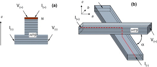
Schematics of a conventional mesa (a), and of a twisted Josephson junction fabricated from whiskers (b). Also indicated in (b) are HTS lattice parameters, the layered structure composed of alternative superconducting (S) and normal (insulating, I) blocks and the current path through the S-I-S layers.
Figure 9.

A composite hierarchical tree like structure of α-MoO3 whiskers on a sillimanite fiber (silicon-aluminium oxide, SAO; see SEM image) and the growth through the vapor transport. Lattice parameters are indicated for MoO3.
One direction of much activity and potential for applied superconductivity is fabrication of HTS coated conductors. To answer why superconducting coated conductors (so-called second-generation conductors) are important and expected to exceed the working characteristics of the current commercial powder-in-tube conductors (first generation conductors) we shall first look at the crystal structure of the HTS cuprates. They all have a layered structure of Cu–O superconducting blocks and non-superconducting blocks alternating along the c-axis. This structure results in highly anisotropic properties. A large conventional single crystal with perfect Cu–O planes would be an ideal conductor of a superconducting current along the ab-plane, Iab . On the other hand, in the real HTS granular material, it is well known that high-angle grain boundaries even in the c-axis textured material (e.g. powder-in-tube conductors) are not perfectly transparent to the passing Iab . This happens because of low coherence length in HTS, which is shorter than the grain boundary thickness. However, in the epitaxial and c-axis oriented thin films, the path of easy current flow is preserved in the ab-plane because of the continuity of Cu–O planes (figure 8(a)). Such 3D epitaxial films of kilometer length are the basis for the coated conductors and they resemble a single crystal. A certain wavy morphology of the grain boundaries in the c-axis oriented conductors may, however, support the flow of the superconducting current [32]; it allows the presence of certain high-angle boundaries, but still requires complex growth control.
Another important problem is related to pinning and vortex motion. HTSs are type-II superconductors and their crystal structure contains non-superconducting blocks. Magnetic field can penetrate HTS and this penetration depends on the direction of the applied magnetic field. Even for the weakest penetration when a magnetic field is perpendicular to the ab-plane, Abrikosov vortices develop and they can easily move (most likely within the ab-plane) resulting in undesired dissipation. To pin the vortices, convenient and good candidates are columnar defects with their axis parallel to the c-axis of the 3D epitaxial HTS films. Size, distribution, density, type of the columnar structures and of the associated nanodefects are essential for pinning and for improvement of the critical current density, Jc, in HTS thin films and coated conductors. The introduction in a controlled way of pinning sites into superconductors is called ‘pinning engineering’. One of the first methods of introducing 1D columnar defects was irradiation with energetic particles [33]. This method was efficient but impractical, and therefore, was abandoned in favor of other techniques. One early example is the growth of an array of MgO nanowires perpendicular to the surface of the substrate [34]. Some of our recent results [35] are shown in figure 10. On the substrate with nanowires a thin HTS film is grown. Another early method is the growth of self-assembled nanodots of different materials on the surface of the substrate. These nanodots can be of artificial type, e.g. Ag grown by physico-chemical deposition methods [36, 37] (figure 11(a)) or of natural type such as Ca [38] (figure 11(b)). Calcium is a common impurity in the low-quality single crystal MgO substrate and precipitates on the surface of the MgO substrate when heating the substrate at high temperatures. Films of HTS are deposited on substrates with nanodots and it is considered that from the top of the nanodot a dislocation parallel to c-axis of the film develops and plays the role of the columnar defect significantly enhancing Jc (figure 12). Nanodots were also produced by surface reconstruction of the substrates or buffers (e.g. CeO2 [39]) under controlled annealing or precipitation of a certain phase as nanodots (e.g. Y2O3 in Y123 HTS films [40]). Precipitation of oriented nanorods (e.g. BaZrO3 in Y-123 [41]) was also demonstrated. New approaches to control pinning can be imagined and it is expected significant progress. Advantages are in the independent control of pinning significantly increasing transport characteristics, while single crystal high quality properties are preserved. It should be noted that crystal perfection depends on the growth mode, very often this being specific for a certain growth technology. In fact, there is a complex relationship between the film growth (method), defects, nanodots/rods/precipitates features, growth of nanodots/rods/precipitates and superconducting practical characteristics of the films or coated conductors. The image of pinning engineering in HTS we have presented is rather simplified to show the current trend in this field of applied superconductivity. Some details of these complex relationships can be found in recent review articles on coated conductors [42] and on nanodots for pinning in HTS [43].
Figure 10.

Self-assembled Au nanodots (atomic force microscopy, AFM, image) grown by PLD on a substrate and used as a template for further growth of MgO array of nanowires (SEM image to the right).
Figure 11.

Self-assembled Ag nanodots grown by rf sputtering on (001)SrTiO3 single-crystal substrate with terraces and natural Ca nanodots precipitated on the surface of the (001)MgO substrate.
Figure 12.

Critical current density plotted versus magnetic field for Tl-1223 HTS (Tl–Ba–Ca–Cu–O and Tl–Ba–Sr–Ca–Cu–O) grown on (001)SrTiO3 substrates with and without nanodots (NDs). Arrows indicate the enhancement of Jc.
Nanodots can be useful for some other purposes in applied superconductivity. We proposed the use of nanodots to reduce the noise in electronics devices such as SQUID [44]. A different idea starting from the growth features of the nanodots is addressed in the next paragraph. The accumulated experience with nanodots and superconductors can be relevant for other materials and their applications.
For applications of thin films in HTS electronics devices, the most used is the conventional mesa geometry (figure 8(a)). It implies the growth of composite layered structures as well as integration possibilities. For multicomponent materials and heterostructures based on HTS, magneto resistant oxides such as manganites or molibdates there is always the problem of obtaining films with flat and clean surfaces without precipitates or segregates. Precipitates-segregates are Cu-rich phases for HTS (figure 14(a)) or Mn-rich phases for manganites.
Figure 14.

(a) Optical microscopy image of the surface of a SmBa2Cu3O7 film grown by MOCVD. (b) Schematic drawing showing the principle of ‘double migration length’ for the precipitate removal in the growth of a film on a substrate with artificial steps. (c) and (d): Optical images of the Bi-2223 films grown on substrates containing artificial steps of the respective widths of 60 and 20 μm. For the 60 μm step, 10 μm-wide regions at the step edge (dashes in panel c) are free of precipitates. At the step width of 20 μm, the entire step is free of precipitates and the condition of ‘double migration length’ is fulfilled. (e) and (f) show substrates with steps (60 and 20 μm) indicated by circles. Substrate (f) was used for the growth of precipitate-free HTS thin films. On these films successful fabrication of intrinsic Josephson junctions with mesa geometry was demonstrated in [47].
Before presenting our solution to the removal of the undesired precipitates-segregates we shall observe in figure 11 the following: nanodots from figure 11(a) are aligned following the terraces of the substrate, while in the figure 11(b) there are no terraces and the location of the nanodots is random. A closer look on the aligned nanodots shows that they are preferentially located at the edge or at the center of a terrace. For certain growth conditions and substrates with terraces, one can obtain (figure 13) nanodots connected into a network of parallel nanowalls (nanowires). The conclusion is that by controlling the substrate surface (e.g. terraces) and growth technological parameters it is possible to engineer the precise location of the nanodot. This approach is expected to be an important future step for controlled pinning in the films, further enhancing Jc, or improving tuning possibilities of Jc.
Figure 13.

AFM image of the parallel Ag nanowalls (wires) grown by rf sputtering on (100)SrTiO3 with terraces.
A similar idea was used to remove the undesired precipitates/segregates on the surface of the film during its deposition. We used artificial steps fabricated by ion milling on the substrate surface [45]. The concept (figure 14(b)) is that the width of steps should be smaller than the double of the migration length of the atomic species deposited on the substrate. For the ‘double migration condition’, the distance to the step edges is sufficiently small so that all precipitates/segregates can migrate and attach to the step edges because the free energy is the lowest at these locations. For HTS such as BSCCO and RE-123 (RE=Y, Sm), this translates in depositing films on steps with the width of about 20 μm (figure 14). For manganites such as La1−xSrxMnO3 the step width should be about 7 μm [46]. The film parts grown on the steps are clean and can be used for device fabrication or integration. This method has several advantages: it is simple, independent of deposition technique and materials of the film and substrate. It does not require changing the established technology, and thus, the investment costs are low. Steps can have any shape and can be obtained by any method as long as the rule of ‘double migration length’ is obeyed. By using substrates with predefined width and depositing films at different temperatures, parameters such as surface diffusion length and activation energy can be experimentally extracted.
Another problem in the thin films growth of multicomponent materials is the roughness of the surface. For HTS thin films by vapor-deposition methods the growth is by a layer-by-layer growth mechanism. Each layer has the thickness of half the c-axis lattice parameter for Bi-2212 or Bi-2223 HTS phases. But, most reports show a roughness of (m×c/2), where m is an integer usually being larger than 3 (figure 15(a)). The meaning is that atomic species arriving on the substrate cannot migrate on the surface (surface diffusion) and generate complete and flat layers. The idea in this case is to give more time for surface spreading and growth of continuous flat layers before the next layer is deposited. The method of ‘interrupted growth’ yielded excellent results, and superconducting films of Bi-2223 with roughness less than c/2 were obtained [47] (figure 15(b)). ‘Interrupted growth’ consists of on/off cycles of deposition. During the off-state the growth conditions are not changed and just a shutter is used to temporary stop the deposition of the film. This method was proposed and initially thought to be specific for pulsed laser deposition (PLD) or layer-by-layer growth of heterostructures by molecular beam epitaxy (MBE) [48, 49]. We demonstrated that it can also be successful for the metal-organic chemical vapor deposition (MOCVD) growth of HTS and that the principles of supersaturation and migration control apply to various growth methods. The advantages of the interrupted growth are simplicity, universality (at least for thin films growing through a 2D layer-by-layer growth mechanism), and compatibility with existing technologies.
Figure 15.

AFM images of Bi-2223 MOCVD thin films grown by (a) conventional continuous deposition and (b) interrupted growth. Height profiles along the indicated lines are presented in the bottom panels.
Wires of Nb3Sn (MT methods)
The superconductor industry is currently relying on Nb3Sn superconducting wires. They are composites with Nb3Sn filaments embedded in a matrix of other materials, which serve various functions, such as barrier, thermal stabilizer, and mechanical reinforcement. Nb3Sn is very sensitive to strain/stress that suppresses superconductivity. After bringing them to the final desired shape through multistep mechanical processing, the Nb3Sn composite wires are reacted at 600–700 °C, and then used at low temperatures. Therefore, owing to the different thermal expansion coefficients of the materials from the composite wire, the residual compressive strain/stress on the Nb3Sn filaments cannot be avoided. Noteworthy, residual stress/strain occurrence is specific for many composites and generates different problems. Cycles of multiple loading–unloading mechanical treatments were proposed. They were designed to induce stepwise plastic deformations of the plastic materials from the composite wire and, through this, gradually to release the compressive strain without breaking the brittle Nb3Sn filaments. The goal is to obtain a zero-strain state for all Nb3Sn filaments in the composite wire. This is not trivial and requires controlled 3D spatial distribution of the loading force. 1D and 2D loadings of tensile and bending type were proposed in [50, 51], respectively. Bending cycles have the advantage that they can apply to industrial processing by passing the wire between pulleys of certain diameters (figure 16).
Figure 16.

Arrangement of pulleys for release of the residual strain in the composite Nb3Sn superconducting wires.
We have also proposed cycles of 3D type realized by applying loading–unloading cycles of torsion or combinations of torsion and bending [52, 53]. Complex 3D (bending + torsion) mechanical treatment of different commercial wires improved their critical superconducting characteristics toward the theoretical limits (figure 17). 3D mechanical treatments can be also easily applied at industrial scale, for example, by controlling the rotation speed of the wire passing through the pulleys. The improved superconducting characteristics of the wires directly translate into higher magnetic fields generated by the react-and-wind magnetic coils. Remarkable is that 3D complex mechanical processing approach is universal (it does not depend on Nb3Sn wires type), simple, and can easily be scaled up to an industrial level with very low investment cost. By its nature, it is independent, i.e. it requires no changes to the current technology for Nb3Sn wire synthesis/processing and coil fabrication. Torsion loading might also be useful for studying the quantitative dependence of the superconducting characteristics on strain. We have also shown that these ideas can be applied to the fabrication (knitting) of strain-free Nb3Sn cables [54, 55].
Figure 17.

Mechanical treatments of (a) Nb3Sn wire produced by Furukawa Electric Co. Ltd, Japan. (b) and (c): The experimental arrangements for torsion and bending on short samples, respectively (1, press to fix the wire; 2, quartz tube; 3, Nb3Sn wire; 4, holder). (d) Critical current, Ic, plotted versus applied magnetic field, B, for the following wires: as-reacted, after cycles of alternate bending (15 times with an optimum bending strain ε=0.8%, B n15(0.8)), alternate torsion (15 times with an optimum torsion angle ϕ=60°, T n15/60°) and alternate torsion and bending (6 torsion and 9 bending steps in the following sequence 3×[(ϕ=60° ×n=2)+ (ε=0.8% ×n=2)+(ε=0.2% ×n=1)], T+B n15). The enhancement of Ic after mechanical processing is indicated by the arrow.
Conclusions
The presented results suggest that correct identification of the problem is necessary for designing a technological solution that would minimize the disadvantages of a certain material. Different unconventional technologies were briefly presented and they have much in common. They are based on concepts and approaches that obey the following criteria:
simplicity (easy to apply),
universality (does not depend on processing methods and can be applied to many materials),
independence from current technologies (there is no need to modify, reconsider or re-optimize current technologies), and they are
surprising, innovative, smart, powerful and allow new possibilities of growth/ processing/ properties control.
Application of such technologies results in different important advantages such as:
new industrial developments or easy integration with the current technologies;
cost-saving by reduction of the necessary time and effort to readjust or upgrade the existing technologies. They are also working against the necessity to invest in sophisticated and expensive processing technologies and equipment;
generation of high quality materials, materials with new properties or new materials otherwise not available;
generation of new ideas (and problems) in fundamental and applied sciences.
It is noteworthy that for many new unconventional technologies the fundamental aspects are still not well understood (e.g. growth under electrical and magnetic fields, nanoblast, superconductivity–train–rocessing relationship, vortex phase diagram in general and versus processing). Further materials synthesis/processing progress for these methods is expected, but at the same time, a sustained research on indicated unconventional methods is mandatory with and without involvement of superconductors.
We also conclude that apart from their value for applications in different fields (power, energy, medicine, transportation, fast electronics and communications) superconductors are playing a major role in development of materials science.
The criteria from the conclusions can be taken for a definition of a ‘beautiful’ technology in materials science.
Acknowledgment
AC acknowledges the financial support of the European Commission through the Marie Curie Excellence Grant MEXT-CT-2006-041111 ‘NanoTechPinningHTS’, the ESF-NES Network. PB acknowledges financial support from Alexander von Humboldt Foundation and MANA. PB and GA acknowledge financial support from PNII PCCE 239/2008-9/2010, Romania. PB, SA and KW acknowledge financial support from NEDO, Japan. The authors are grateful for collaboration, technical assistance, useful discussions and encouragement received from the members of several groups at NIMP, METAV, AIST, NIMS, Mainz University, University of California (Davis), Tohoku University, National Technical University of Ukraine (KPI), University of Sao Paulo, and Normal University of Beijing. PB, SA and KW thank Furukawa Electric Co Ltd for providing samples of N3Sn wires.
References
- Aigner M. 2008. Presentation at Alexander von Humboldt Annual Meeting (Berlin, Germany, 16 June) [Google Scholar]
- Gelernte D. Machine Beauty: Elegance and the heart of technology. New York Basic Books, A Member of Perseus Books Groups; 1998. ISBN 0-465-04516-2 [Google Scholar]
- Badica P, Aldica G. and Mandache S. Supercond. Sci. Technol. 1999;12:162. doi: 10.1088/0953-2048/12/3/010. [DOI] [Google Scholar]
- Badica P. and Aldica G. J. Optoelectron. Adv. Mater. 2003;5:1029. [Google Scholar]
- Yavuz M, Maeda H, Vance L, Liu H K. and Dou S X. Supercond. Sci. Technol. 1998;11:1166. doi: 10.1088/0953-2048/11/10/058. [DOI] [Google Scholar]
- Primo V, Sapina F, Sanchis M J, Ibanez R, Beltran A. and Beltran D. Solid State Ionics. 1993;63:872. doi: 10.1016/0167-2738(93)90209-L. [DOI] [Google Scholar]
- Aldica G. and Badica P. Rom. J. Phys. 2000;45:493. [Google Scholar]
- Iurchenko I A, Alexeev A F, Yurchenko D O, Badica P, Gridasova T Y, Morozov V V, Nemirovsky A V. and Peklun V F. Physica. 2003;384(C):111. doi: 10.1016/S0921-4534(02)01804-X. [DOI] [Google Scholar]
- Badica P, Aldica G, Groza J R, Bunescu M-C. and Mandache S. Supercond. Sci. Technol. 2002;15:32. doi: 10.1088/0953-2048/15/1/307. [DOI] [Google Scholar]
- Groza J R. and Zavaliangos A. Mater. Sci. Eng. 2000;287(A):171. doi: 10.1016/S0921-5093(00)00771-1. [DOI] [Google Scholar]
- Sandu V, Aldica G, Badica P, Groza J R. and Nita P. Supercond. Sci. Technol. 2007;20:836. doi: 10.1088/0953-2048/20/8/020. [DOI] [Google Scholar]
- Hulbert D M, Anders A, Dudina D V, Andersson J, Jiang D, Unuvar C, Anselmi-Tamburini U, Lavernia E. and Mukherjee A K. J. Appl. Phys. 2008;104:033305. doi: 10.1063/1.2963701. [DOI] [Google Scholar]
- Raitchenko A I. Osnovi protzhessa spekania poroshkov propuskaniem electritcheskovo toka ed. ‘Metallurghia’, 128 pages (in Russian) 1987 [Google Scholar]
- Grasso S, Sakka Y. and Maizza G. Sci. Technol. Adv. Mater. 2009;10:053001. doi: 10.1088/1468-6996/10/5/053001. [DOI] [PMC free article] [PubMed] [Google Scholar]
- Aldica G, Sandu V, Plapcianu C, Badica P. and Groza J R. J. Phys.: Conf. Series. 2009;150:052006. doi: 10.1088/1742-6596/150/5/052006. [DOI] [Google Scholar]
- Miu L, Aldica G, Badica P, Ivan I, Miu D. and Jakob G. Supercond. Sci. Technol. 2010;23:095002. doi: 10.1088/0953-2048/23/9/095002. [DOI] [Google Scholar]
- Dou S X, Soltanian S, Horvat J, Wang X L, Zhou S H, Ionescu M, Liu H K, Munroe P. and Tomsic M. Appl. Phys. Lett. 2002;81:3419. doi: 10.1063/1.1517398. [DOI] [Google Scholar]
- Lim H J, Jang S H, Hwang S M, Choi J H, Joo J, Kang W N. and Kim C. Physica. 2008;468(C):18. [Google Scholar]
- Vasylkiv O. and Sakka Y. Nano Lett. 2005;5:2598. doi: 10.1021/nl052045+. [DOI] [PubMed] [Google Scholar]
- Vasylkiv O, Borodianska H, Badica P, Zhen Y. and Tok A. J. Nanosci. Nanotechnol. 2009;9:141. doi: 10.1166/jnn.2009.J008. [DOI] [PubMed] [Google Scholar]
- Sundaresan A, Bhargavi R, Rangarajan N, Siddesh U. and Rao C N R. Phy. Rev. 2006;74(B):161306. doi: 10.1103/PhysRevB.74.161306. [DOI] [Google Scholar]
- Borodianska H, Badica P, Uchikoshi T, Sakka Y. and Vasylkiv O. J. Alloys Comp. 2011;509:2535. doi: 10.1016/j.jallcom.2010.11.079. [DOI] [Google Scholar]
- Badica P, Togano K, Awaji S, Watanabe K. and Kumakura H. Supercond. Sci Technol. 2006;19:R81. doi: 10.1088/0953-2048/19/10/R01. [DOI] [Google Scholar]
- Chen W M. Phys. Rev. 1998;57(B):7503. doi: 10.1103/PhysRevB.57.7503. [DOI] [Google Scholar]
- Awaji S, Ma Y, Chen W P, Maeda H, Watanabe K. and Motokawa M. Curr. Appl. Phys. 2003;3:391. doi: 10.1016/S1567-1739(03)00097-X. [DOI] [Google Scholar]
- Derango P, Lees M, Lejay P, Suplica A, Tournier R, Ingold M, Germi P. and Pernet M. Nature. 1991;349:770. doi: 10.1038/349770a0. [DOI] [Google Scholar]
- Badica P, Togano K, Awaji S, Watanabe K, Iyo A. and Kumakura H. J. Cryst. Growth. 2004;269:518. doi: 10.1016/j.jcrysgro.2004.05.115. [DOI] [Google Scholar]
- Badica P. and Togano K. J. Mater. Res. 2005;20:3358. doi: 10.1557/jmr.2005.0413. [DOI] [Google Scholar]
- Awaji S, Inoue T, Takahashi K, Badica P, Nishijima G. and Watanabe K. IEEE Trans. Appl. Supercond. 2009;19:3071. doi: 10.1109/TASC.2009.2018211. [DOI] [Google Scholar]
- Takano Y, Hatano T, Fukuyo A, Ishii A, Arisawa S, Tachiki M. and Togano K. Supercond. Sci. Technol. 2001;14:765. doi: 10.1088/0953-2048/14/9/327. [DOI] [Google Scholar]
- Badica P. Cryst. Growth Design. 2007;7:794. doi: 10.1021/cg060893s. [DOI] [Google Scholar]
- Feldmann D M, Holesinger T G, Feenstra R. and Larbalestier D C. J. Am. Ceram. Soc. 2008;91:1869. doi: 10.1111/j.1551-2916.2008.02273.x. [DOI] [Google Scholar]
- Civale L, Marwick A D, Worthington T K, Kirk M A, Thomson J R, Krusinelbaum L, Sun Y, Clem J R. and Holtzberg F. Phys. Rev. Lett. 1991;67:648. doi: 10.1103/PhysRevLett.67.648. [DOI] [PubMed] [Google Scholar]
- Yang P D. and Lieber C M. J. Mater. Res. 1997;12:2981. doi: 10.1557/JMR.1997.0393. [DOI] [Google Scholar]
- Crisan A, Tanner J L, Mikheenko P. and Abell J S. Optoelectron. Adv. Mater.—Rapid Commun. 2009;3:231. [Google Scholar]
- Crisan A, Fujiwara S, Nie J C, Sundaresan A. and Ihara H. Appl. Phys. Lett. 2001;79:4547. doi: 10.1063/1.1428632. [DOI] [Google Scholar]
- Crisan A, Badica P, Fujiwara S, Nie J C, Sundaresan A, Iyo A. and Tanaka Y. IEEE Trans. Appl. Supercond. 2003;13:3726. doi: 10.1109/TASC.2003.812527. [DOI] [Google Scholar]
- Badica P, Sundaresan A, Crisan A, Nie J C, Hirai M, Fujiwara S, Kito H. and Ihara H. Physica. 2003;383(C):482. doi: 10.1016/S0921-4534(02)01836-1. [DOI] [Google Scholar]
- Nie J C, Yamasaki H, Yamada H, Nakagawa Y, Develos-Bagarinao K. and Mawatari Y. Supercond. Sci. Technol. 2004;17:845. doi: 10.1088/0953-2048/17/7/005. [DOI] [Google Scholar]
- Haugan T, Barnes P N, Wheeler R, Meisenkothen F. and Sumption M. Nature. 2004;430:867. doi: 10.1038/nature02792. [DOI] [PubMed] [Google Scholar]
- McManus-Driscoll J L.et al Nat. Mater. 2004;3:439. doi: 10.1038/nmat1156. [DOI] [PubMed] [Google Scholar]
- Holesinger T G.et al Adv. Mater. 2008;20:391. doi: 10.1002/(ISSN)1521-4095. [DOI] [Google Scholar]
- Matsumoto K. and Mele P. Supercond. Sci. Technol. 2010;23:014001. doi: 10.1088/0953-2048/23/1/014001. [DOI] [Google Scholar]
- Crisan A, Badica P, Fujiwara S, Nie J C, Sundaresan A, Tanaka Y. and Ihara H. Appl. Phys. Lett. 2002;80:3566. doi: 10.1063/1.1478782. [DOI] [Google Scholar]
- Endo K, Badica P, Sato H. and Akoh H. Adv. Mater. 2004;16:1894. doi: 10.1002/(ISSN)1521-4095. [DOI] [Google Scholar]
- Ishii Y, Sato H, Sawa A, Yamada T, Akoh H, Endo K, Kawasaki M. and Tokura Y. Appl. Phys. Lett. 2004;85:3800. doi: 10.1063/1.1807969. [DOI] [Google Scholar]
- Endo K, Badica P, Sato H. and Akoh H. Supercond. Sci. Technol. 2006;19:S221. doi: 10.1088/0953-2048/19/5/S12. [DOI] [Google Scholar]
- Koster G, Rijnders G J H M, Blank D H A. and Rogalla H. Appl. Phys. Lett. 1999;74:3729. doi: 10.1063/1.123235. [DOI] [Google Scholar]
- Bove P, Rogersand D J. and Hosseini Teherani F. J. Cryst. Growth. 2000;220:68. doi: 10.1016/S0022-0248(00)00639-4. [DOI] [Google Scholar]
- Ochiai S. and Osamura K. Cryogenics. 1992;32:584. doi: 10.1016/0011-2275(92)90045-C. [DOI] [Google Scholar]
- Awaji S, Watanabe K. and Katagiri K. Supercond. Sci. Technol. 2003;16:733. doi: 10.1088/0953-2048/16/6/313. [DOI] [Google Scholar]
- Badica P, Oguro H, Awaji S, Nishijima G. and Watanabe K. J. Phys: Conf. Ser. 2008;97:012036. doi: 10.1088/1742-6596/97/1/012036. [DOI] [Google Scholar]
- Badica P, Oguro H, Awaji S, Nishijima G. and Watanabe K. Supercond. Sci. Technol. 2007;20:810. doi: 10.1088/0953-2048/20/8/015. [DOI] [Google Scholar]
- Watanabe K, Oguro H, Badica P, Awaji S, Nishijima G, Tsubouchi H. and Meguro S. J. Phys: Conf. Ser. 2008;97:012008. doi: 10.1088/1742-6596/97/1/012008. [DOI] [Google Scholar]
- Awaji S, Watanabe K, Oguro H, Nishijima G, Tsubouchi H, Miyoshi K. and Meguro S. Fusion Eng. Design. 2006;81:2473. doi: 10.1016/j.fusengdes.2006.07.058. [DOI] [Google Scholar]