Abstract
Recent progress in photoactive organic field-effect transistors (OFETs) is reviewed. Photoactive OFETs are divided into light-emitting (LE) and light-receiving (LR) OFETs. In the first part, LE-OFETs are reviewed from the viewpoint of the evolution of device structures. Device performances have improved in the last decade with the evolution of device structures from single-layer unipolar to multi-layer ambipolar transistors. In the second part, various kinds of LR-OFETs are featured. These are categorized according to their functionalities: phototransistors, non-volatile optical memories, and photochromism-based transistors. For both, various device configurations are introduced: thin-film based transistors for practical applications, single-crystalline transistors to investigate fundamental physics, nanowires, multi-layers, and vertical transistors based on new concepts.
Keywords: Organic field-effect transistor, Phototransistor, Light-emitting transistor, Optical memory, Photochromism
Introduction
Organic electronic devices have been extensively investigated owing to their many potential advantages, including cost effectiveness, large-scale manufacture, wet processability, and mechanical compatibility with flexible displays. These advantages make it possible to open a new paradigm called ‘plastic electronics’, which is expected to complement silicon electronics [1–5]. The organic field-effect transistor (OFET) is a key device of plastic electronics [6–8]. After many years of efforts to develop new organic compounds [9, 10] and thin-film growth techniques [11, 12], field-effect carrier mobility has reached 20 cm2 Vs−1, which is high enough for practical applications [13]. These high performances have been achieved in thin films prepared under well-optimized conditions, including deposition temperature and growth rate [14]. The next stage for commercialization is to establish a cost-effective process for large-scale device integration. In addition, a new trend has recently appeared for incorporating novel functionalities into conventional OFETs. Various functions derived from organic molecules are integrated into OFETs; e.g., gas sensing, optical switching, memory, spintronics, and light emission [15–21]. These functionalities can be realized owing to the diversity of organic materials. For example, molecular structures, whether small molecules or polymeric materials, can be designed according to required functions. Among optical functionalities in particular, molecular structures are tuned to adjust light-emitting and light-absorbing wavelengths. These diversities are strong points of organic materials.
This article reviews photoactive OFETs, in which optical functionalities are incorporated into conventional transistors. Photoactive OFETs can be categorized into light-emitting and light-receiving OFETs, as summarized in figure 1. An essential point of light-emitting OFETs (LE-OFETs) is how to enhance carrier recombination between electrons and holes. Light emissivity, injection of holes and electrons, and their transport should be well balanced. From this viewpoint, ambipolar transistors are more advantageous than unipolar ones. Additionally, novel device structures have been proposed recently, with the aim of improving these factors. The major merits of light-receiving OFETs (LR-OFETs) are the wide wavelength range of light absorption and the high responsivity of organic materials to light stimulation. Light signals can be effectively converted into electrical current and amplified in the transistor structures. These merits enable us to develop various LR-OFETs, such as phototransistors, and non-volatile memory and optical switching devices. Phototransistors show the effective photoelectric conversion of the organic materials to the fullest. Non-volatile memory and photochromism in transistors have other fascinating characteristics: light irradiation permits multi-level memory and switching, which are unavailable in inorganic counterparts.
Figure 1.
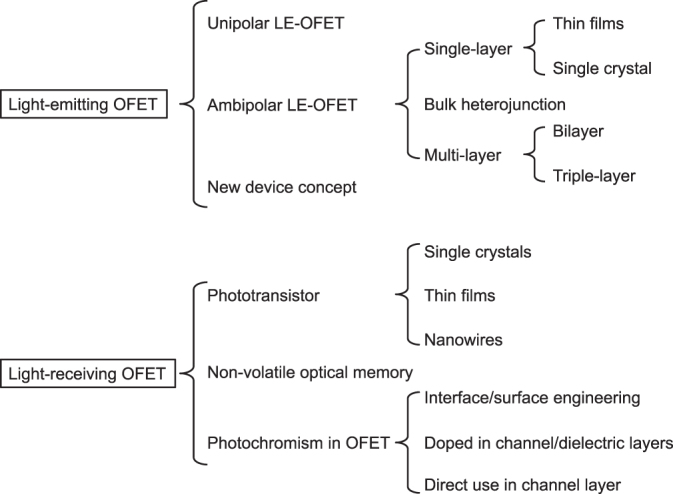
Categorization of photoactive organic field-effect transistors (OFETs).
The first part of this article focuses on the LE-OFETs, with an emphasis on the evolution of the device structures from single-layered unipolar to multi-layered ambipolar transistors. The second part features the LR-OFETs, in which the diversity of molecular functions enables various device operations, including optical sensors, memory, and switches.
Light-emitting OFETs
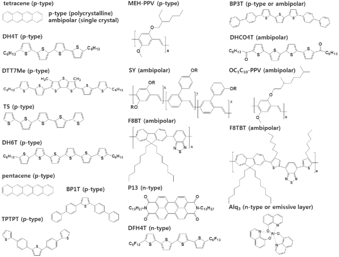
LE-OFETs combine functions of both organic light-emitting diodes (OLEDs) and OFETs. Since the creation of the first LE-OFET from tetracene thin films [22], novel combinations of both electrical switching and light-emitting properties in an individual organic transistor have allowed new functional optoelectronic devices. Electrical switching is enabled by modulation of the current flow between the source and drain electrodes under tuned gate bias voltage, while electroluminescence (EL) takes place by electron–hole recombination in the transistor channel. One approach to LE-OFET development is to optimize device configurations to balance these physical phenomena. Another approach is to design chemical structures for the transistor channels. Figure 2 shows the chemical structures of LE-OFETs. Positively charged electric carriers (holes) are dominant in the organic semiconductors with large ionization energy. These hole transport materials are referred to as p-type semiconductors while organic semiconductors with large electron affinities allow electron transport and are categorized as n-type semiconductors. Some of them can transport both holes and electrons; these are ambipolar semiconductors. The active layers, in which holes and electrons are transported and recombine to emit light, are composed of a single material or a combination of these heterogeneous materials. Such device structures have been realized with a number of molecular and polymeric semiconductors by thermal evaporation or solution processes.
Figure 2.
Chemical structures of organic compounds for LE-OFETs.
In addition, LE-OFETs are considered as excellent systems to investigate physical processes such as charge-carrier injection, exciton formation, energy/charge transfer, charge trapping, and electroluminescence in organic-based devices [23–25]. A full understanding of these processes would provide not only opportunities to simplify circuit design, but also new potential applications of organic semiconductors, such as highly integrated optoelectronics and electrically pumped organic lasers [17]. This section describes various approaches to developing these features in LE-OFETs.
Unipolar LE-OFET
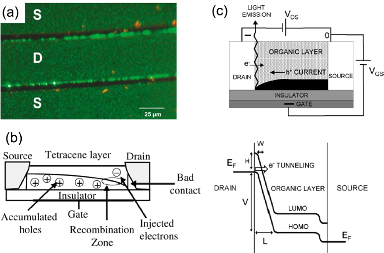
Tetracene is a representative OFET material of the acene family with an EL characteristic. Hepp et al first observed light emission in a single-layered tetracene FET [22]. LE-OFET devices with an interdigitated pattern of gold source and drain electrodes were fabricated in a bottom-gate and bottom-contact configuration. Importantly, the light emission was observed only along the drain electrode (figure 3(a)); carrier recombination occurred in the tetracene film near the drain electrode. The emission spectrum of this device coincides with the typical light emission from a tetracene thin film, with a peak at 540 nm. In this unipolar device, the major carriers are holes. The question is how electrons are injected into the tetracene film. Hepp et al considered that the charge injection mechanisms (supplying holes from the source and electrons from the drain) are different owing to imperfections in the electrical contact. They attributed electron injection into the tetracene layer to poor contact at the electrode–organic interface (figure 3(b)). On the other hand, Santato et al explained the electron injection by a phenomenological model: a steep voltage drop at the drain–tetracene interface causes a distortion in the highest occupied molecular orbital (HOMO) and the lowest unoccupied molecular orbital (LUMO) of tetracene molecules, which induces electron tunneling from the metal work function level to the LUMO of tetracene [26]. The device structure and an energy level diagram are given in figure 3(c). In this manner, the mismatch in the carrier injection is a drawback of the unipolar LE-OFETs.
Figure 3.
(a) Optical image of electroluminescence. (b) Schematic view of carrier processes, including hole accumulation, electron injection, and electron–hole recombination in the tetracene-based LE-OFET. Reprinted from [22] with permission; © 2003, American Physical Society. (c) Working principle of an LE-FET device. The main electronic process takes place when the device is operated in standard p-type mode. Energy-level diagram shows the mechanism of electron injection from the drain electrode into the organic layer. Reprinted from [26] with permission; © 2004, Elsevier.
Early in LE-OFET development, excellent breakthroughs were reported in relation to organic electronics. One of them was flexibility of devices. Muccini’s group developed a tetracene-based LE-OFET on a flexible, transparent plastic film, which worked as both substrate and gate dielectric. LE-OFETs on plastic substrates thus opened a way to flexible devices combining the switching function of a transistor and light emission [27]. Another breakthrough was the solution process for producing organic devices based on oligothiophene compounds [28, 29]. Muccini’s group reported the dithienothiophene derivative 2,6-bis-(5′-hexyl-[2,2′]bithiophen-5-yl)-3,5-dimethyl-dithieno[3,2-b;2′,3′-d]thiophene (DTT7Me). LE-OFETs were successfully fabricated by drop casting [29]. This is the first demonstration of a solution-processed LE-OFET based on non-polymeric materials.
Ambipolar LE-OFET
As mentioned above, an imbalance in carrier injection and transport in unipolar transistors inhibits light emission. Device configurations should be optimized to address this problem. Figure 4 illustrates typical configurations of LE-OFETs [23, 30]: single-layer, bulk heterojunction, and bilayer structures. The device structures are composed of a single organic layer, which is capable of transporting electrons as well as holes, or a bilayer of two unipolar transport materials. Both holes and electrons are simultaneously injected into the channel from the electrodes under a suitable gate bias. To realize such ambipolar transistor operation, adequate selection of metal electrode materials is also essential because carrier injection is dependent on the work functions of metals. The position of light emission can be controlled within the channel area depending on the applied gate (Vg) and source-drain voltages (Vds). Well-balanced carrier mobilities between holes and electrons are thus preferred [23–25].
Figure 4.
Schematic illustrations of ambipolar LE-OFETs consisting of (a) single layer, (b) bulk heterojunction, and (c) bilayer heterojunction LE-OFET structures.
Single-layer LE-OFET (thin films, single crystal)
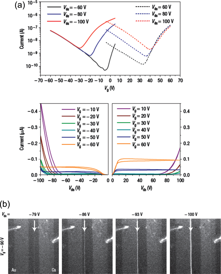
Zaumseil et al developed a single-layer LE-OFET with poly(2-methoxy-5-(3,7-dimethyloctoxy)-p-phenylene-vinylene) (OC1C10-PPV) as an active layer. Characteristic of this device is asymmetric electrodes; Au and Ca electrodes were used for hole and electron injection, respectively [31]. Figure 5(a) shows the typical transfer and output characteristics at various Vds and Vg bias voltages. These results show that both electrons and holes are effectively injected into the active layer. The carrier mobilities of electrons and holes are well balanced, and are estimated to be 3 × 10⁻³ and 6 × 10⁻⁴ cm2 Vs−1, respectively. Figure 5(b) shows the movement of the light emission positions in the OC1C10-PPV layer. As indicated by the arrow, the emission positions shifted with a change in Vds from –79 V to –100 V at a constant gate bias voltage (Vg = −90 V). A narrow line of light appears near the Ca contact when Vds exceeds the threshold bias for an electron accumulation layer. The emission zone moves gradually from the Ca electrode towards the Au electrode with increasing |Vds|. Zaumseil et al also fabricated ambipolar LE-OFETs with poly(9,9-di-n-octylfluorene-alt-benzothiadiazole) (F8BT) and poly((9,9-dioctylfluorene)-2,7-diyl-alt-[4,7-bis(3-hexylthien-5-yl)-2,1,3-benzothiadiazole]-2′,2″-diyl) (F8TBT) [32–38]. On the basis of theoretical models, they clarified that the ambipolar regime can be regarded as a series of saturated electron–hole channels within the transistor channel. The maximum external quantum efficiency of F8BT was 0.8%, which is better than that of single-layer F8BT LED (ca. 0.5%). It is consistent with complete recombination of all charges and a singlet exciton fraction of 25%. According to spin statistics, electron–hole recombination leads to a 25% singlet and 75% triplet state population. In the case of organic molecules, only singlets emit light (fluorescence), while the triplet excitation energy is transferred into heat.
Figure 5.
(a) Transfer and output characteristics of an OC1C10-PPV ambipolar LE-OFET. (b) Digital images of visible light emission from the OC1C10-PPV channel at constant gate voltage (Vg = −90 V) with different Vds. The hole-injecting electrode (Au) and electron-injecting electrode (Ca) are indicated. Reprinted from [31] with permission; © 2006, Nature Publishing Group.
In the abovementioned studies, thin films for the transistors were prepared by solution processes or vacuum deposition. These thin-film-based device and growth processes are suitable for device applications. Separately, single crystals are very useful for fundamental research to understand the nature of carrier transport and recombination as well as light emission because of their perfect lattice structure, although single crystals are far from being of practical use for active layers. For example, Takahashi and co-workers have reported the first ambipolar light-emitting transistor of a tetracene single crystal [39], in which electrons and holes were injected from Mg and Au electrodes and recombined radiatively within the tetracene channel. They demonstrated that the position of the recombination/emission zone could be moved to any position along the channel by varying the applied voltages. An inert atmosphere for device fabrication and effective use of device components, including a single crystal, polymer dielectric layer and asymmetric electrodes (Mg, Au), made possible such well organized experiments.
Bisri et al have successfully demonstrated high-performance ambipolar LE-OFETs that contain various organic single crystals, such as α,ω-bis(biphenylyl)terthiophene (BP3T), rubrene, 4,4′-diphenyl-vinylene-anthracene (DPVA), and tetraphenylpyrene (TPPy). The merits of these materials are strong luminescence and high carrier mobilities, though these properties have been believed to be mutually exclusive [40, 41]. Bright emission was demonstrated through self-waveguide edge emission, which is also achievable by single crystals. The result paves the way for developing electrically driven laser oscillations from organic materials [40].
Nakanotani et al have reported an effect of dye-doping in ambipolar LE-OFETs. Dye-doping of organic crystals permits tuning of the emission color, as well as a significant increase in light emission efficiency [42]. A high light emission was obtained by doping tetracene into a p-distyrylbenzene (P3V2) single crystal, the external EL quantum efficiency of which (∼0.64%) was one order of magnitude higher than that of a non-doped one. They elucidated that the carriers recombined on the light-emissive tetracene molecules in the P3V2 host crystal. They also achieved injection of high current density by interfacial carrier doping based on electron transfer from a five-ring oligo(p-phenylenevinylene)p-bis[(p-styryl) tyryl]-benzene (P5V4) single crystal to a molybdenum oxide layer [43].
Bulk heterojunction LE-OFET
In a bulk heterojunction structure, p-type (hole transport) and n-type (electron transport) semiconducting materials are mixed in a single active layer of the transistor. Rost et al proposed a device structure produced by co-evaporation of a 1:1 ratio of N,N′-ditridecylperylene-3,4,9,10-tetracarboxylic diimide (P13) and α-quinquethiophene (T5) for n-type and p-type material [44, 45]. The formation of excitons is associated with the relative positions of the HOMO and LUMO levels of these materials. These energy level alignments hint at which materials to choose. However, exciton formation competes with charge transport owing to the dispersed interface between these hole and electron transport materials. Compared to the layered configurations (bilayer, triple layer), bulk heterojunction presents one main advantage. The electron and hole flows are interpenetrated in the charge transport region and the p–n interface area is much more extended. This merit can promote recombination probability. However, there is a physical obstacle to efficient charge transport in the active layer [30, 44, 45]. In addition, fine adjustment of the co-evaporation of two materials is essential to obtaining well balanced carrier mobilities and improved electroluminescence.
Multi-layer LE-OFET (bilayer, triple layer)
In general, light emission in LE-OFETs consists of three steps: carrier injection from electrodes, carrier transport through active layers, and recombination at the hetero-interface. Single-layer and bulk heterojunction LE-OFETs are not relevant to these steps, even though the device fabrication processes are simple. This section describes efforts to enhance light emissivity by optimizing the carrier processes (injection, transport and recombination). A key strategy is to share each process by each device component. For this purpose, the numbers of active layers have been increased up to bilayer and triple layers, sacrificing the simplicity of device structure.
A bilayer heterojunction is a typical example of an advanced LE-OFET. In this structure, n-type and p-type semiconducting layers are stacked, and electrons and holes travel in the respective layers (figure 4(c)). Materials and growth conditions of each layer, including organic layers and metal electrodes, can be optimized; as a result, this approach offers the advantage of enhanced carrier injection and mobilities. Dinelli et al reported on a bilayer of α,ω-dihexyl-quaterthiophene (DH4T) and P13 LE-OFET that showed improved ambipolar properties with light emission [46]. The mobility was ca. 3 × 10⁻² cm2 Vs−1, the highest reported to date for ambipolar LE-OFETs, and was achieved by balanced carrier transport. They observed that EL occurred only when the bottom layer was biased by the gate electrode, and that the light emission originated from the P13 upper layer as expected from energetic considerations.
Di et al reported the first observation of visible light emission under ambient atmosphere. They used pentacene and tris-(8-hydroxyquinoline)aluminum (Alq3) as the carrier transport and light-emitting materials, respectively [47]. The laterally arranged heterojunction structures were produced by a successive inclined deposition of respective layers. They obtained light emission with Au and LiF–Al electrodes, but not with Au–Au electrodes. This result indicates that the low work function of LiF–Al electrode is effective for efficient electron injection.
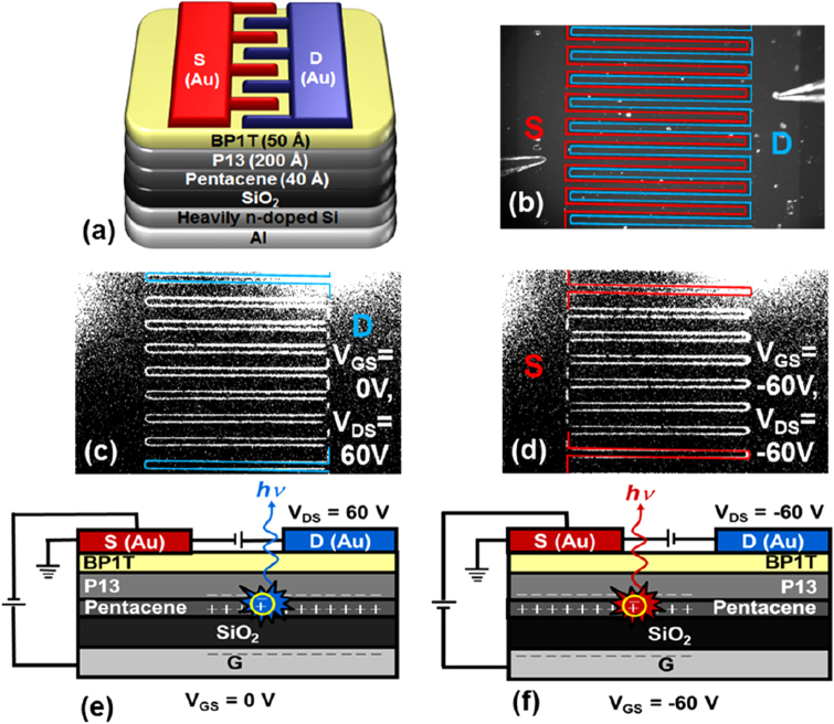
Seo et al developed a series of ambipolar heterojunction-based LE-OFETs with active layer combinations of P13/α,ω-dihexylsexithiophene (DH6T), P13/tetracene, and pentacene/P13/2,5-bis(4-biphenyl) thiophene (BP1T, protective layer) [48–51]. These bilayers were successively deposited by use of a neutral cluster beam deposition (NCBD) method. An example is shown in figures 6(a) and (b). They emphasized that the NCBD technique allowed high-quality thin-film growth, and as a result, the LE-OFETs demonstrated well balanced ambipolarity and operational stability. Clear EL under ambient conditions was obtained, as shown in figures 6(c) and (d). The light-emitting area shifted from the drain side to the source side depending on the gate bias voltage (0 or –60 V). Schemes of carrier recombination and light emission are illustrated in figures 6(e) and (f).
Figure 6.
(a) Schematic view of the pentacene/P13/BP1T-based LE-OFET device. (b) Photograph of device, on which the red and blue lines indicate the source and drain electrodes, respectively. CCD images show light emission from around (c) drain (Vg = 0, Vds = 60 V) and (d) source electrodes (Vg = −60 V, Vds = −60 V). (e), (f) Carrier recombination mechanisms at respective bias voltages. Reprinted from [51] with permission; © 2013, American Chemical Society.
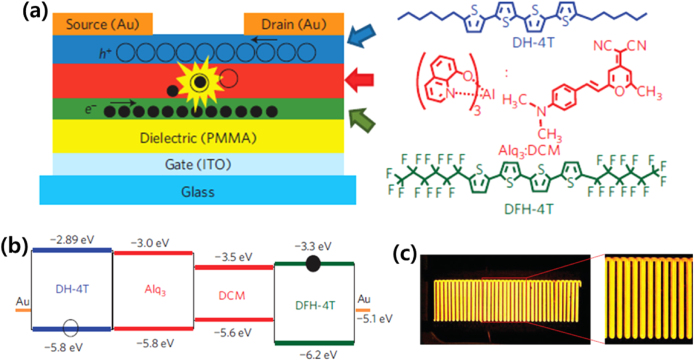
Capelli et al investigated the first triple-layer heterostructure for an LE-OFET. Here, a light-emitting layer, Alq3-doped 4-(dicyanomethylene)-2-methyl-6-(p-dimethylaminostyryl)-4H-pyran dye (DCM), was inserted between p-type (DH4T) and n-type (α,ω-diperfluorohexylquaterthiophene: DFH-4T) layers (figures 7(a), (b)) [52]. This structure enabled simultaneous suppression of electrode-induced photon losses and exciton–metal interaction, as well as exciton–charge interaction. The EL region spread over the channel (figure 7(c)), which was achieved by preventing exciton–metal quenching to reduce photon losses. Furthermore, the emission layer was separated from charge flows to suppress the exciton–charge quenching. Consequently, an external quantum efficiency of 5% was realized, exceeding the best OLEDs based on the same emitting layer and optimized transport layers (2.2%, [53]). In a similar study, they showed that the emission area in a triple-layer LE-OFET (DH4T/Alq3:PtOEP/DHF4T) can be controlled under the gate bias voltage, and the entire channel of the device can emit light [54].
Figure 7.
(a) Schematic illustrations of the device and chemical structures of the triple-layer LE-OFET. ITO stands for indium tin oxide. (b) Energy-level diagram of the triple-layer heterostructure. (C) Optical micrograph of the light emission from the triple-layer LE-OFET (Vds = Vgs = 90 V). Reprinted from [52] with permission; © 2010, Nature Publishing Group.
Heeger’s group have developed a variety of LE-OFETs using ‘Super Yellow’ (SY) material [55–60]. Their triple-layer LE-OFETs consist of a hole-transporting layer, an emissive layer (MEH-PPV, SY, and PFO), and a conjugated polyelectrolyte (CPE) layer. The CPE layer was used as an electron injection layer to improve device performance with stable Au electrodes [55]. The thin CPE layer most likely introduces ordered dipoles at the metal–organic semiconductor interface that facilitate electron injection. They demonstrated multicolor LE-OFET by adjusting different emissive layers. In particular, they reported excellent performance from solution-processed blue-emitting LE-OFETs for the first time.
New concepts of device structures
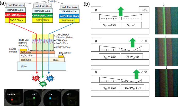
Yang et al reported a vertical LE-OFET [61]. They achieved dual functions, light-emitting diode and electrical switching transistor, by stacking a capacitor layer on an OLED. Rinzler’s group improved the device performance of the vertical LE-OFET, using a carbon nanotube network as the source electrode [62]. They demonstrated LE-OFET operation at low voltage (−3 V) with low power dissipation (6.2%) and a high aperture ratio (98%). Importantly, they demonstrated light emission in the three primary colors (figure 8(a)) [63]. The high-level performance was enabled by use of a single-wall carbon nanotube network that permits the integration of transistor operation and light emission into a single stacked device. The device performance is comparable to that of polycrystalline-silicon-backplane transistor-driven display pixels [64]. In particular, their device structure is a clear departure from conventional LE-OFET designs as it consists of an OLED inserted into a vertical OFET. The new concept design represents a significant step towards solving many outstanding issues in the fabrication of large OLED displays.
Figure 8.
Device structures based on new concepts. (a) Schematics of the vertical LE-OFET with carbon nanotube (CNT) network. Images show red, green, and blue pixels at the indicated gate voltage. DNTT, TFB, TAPC, CBP, mCP, Ir(MDQ)2, Ir(ppy)3, Firpic and 3TPYMB stand for dinaphtho-[2,3-b:2′,3′-f]thieno[3, 2–b]-thiophene, poly(9,9-dioctyl-fluorene-co-N-(4-butylphenyl)-diphenylamine), 1,1-bis[(di-4-tolyamino)phenyl]cyclohexane, 4,4-N,N-dicarbazole-biphenyl, N,N′-dicarbazolyl-3,5-benzene, iridium(III)bis(2-methyldibenzo[f,h]quinoxaline) (acetylacetonate), Fac-tris(2-phenylpyridinato)iridium(III), bis[(4,6-di-fluorophenyl)-pyradinate-N,C2′]picolinate and tris[3-(3-pyridyl)-mesityl]borane, respectively. Reprinted from [63] with permission; © 2011, Science. (b) Schematics of the split-gate LE-OFET and images of the EL zone operated under optimized gate and drain bias voltages. Reprinted from [65] with permission; © 2012 Wiley-VCH, Weinheim, Germany.
Recently, some groups have shown ingenuity in gate electrode architectures. A split-gate LE-OFET proposed by Hsu et al provides a powerful pathway for the active control of charge injection to overcome the passive response of an ambipolar material and to increase EL efficiency [65]. Two gate electrodes inserted in the gate dielectric layer can supply bias voltage independently to break the continuous channel (figure 8(b)). Adjustment of the respective bias can position the brightest luminescent area far from the metal source–drain contacts to avoid exciton quenching. Liu et al reported a dual-gate light-emitting electrochemical transistor [66]. This configuration with a confining p–n junction pushes the light emission area away from the charge-injecting electrodes. The structure also suppresses exciton quenching and enables stable light emission at a specific location within the channel.
Light-receiving OFETs
In general, organic semiconductors absorb light over a wide range, from ultraviolet (UV) to visible. The absorbed light excites the energy states of molecules to produce excitons or to induce molecular conformational changes (i.e., photoisomerization). OFETs effectively convert these light-stimulated states into electrical signals, opening a way to new optoelectronic devices, such as phototransistors, optical memory, and switching devices [15, 20, 67]. These light-receiving OFETs (LR-OFETs) are featured in this section.
Phototransistors
Photogenerated carriers can be collected into the drain electrode under appropriate source–drain and gate bias voltages. Thus, phototransistors have potential for photoelectric conversion devices, optical sensing, and switching devices. The basic device structure is a bottom-gate type, because channel layers receive light from the top. The three-terminal device configuration of transistors offers advantages over two-terminal diodes because transistors can reduce noise and amplify the electrical signal. Therefore, organic compounds for phototransistors require both high light sensitivity and high carrier mobility.
The performance of phototransistors is evaluated by parameters of photoresponsivity (R = (Ilight − Idark)/L) and photosensitivity (P = (Ilight − Idark)/Idark), where Ilight and Idark represent drain current under light and dark conditions, and L is the intensity of irradiated light. P depends on L, but R depends only on wavelength, and is normalized by L. Thus, the value of R is comparable to those of other phototransistors. Assessment criterion of R is 300 A W−1, because this value has been reported from a conventional single-crystal Si phototransistor. To overcome this criterion, various device types have been developed. This section summarizes recent progress in organic phototransistors of three device types: single crystals, thin films, and nanowires.
Single-crystal phototransistors
Single crystals allow us to explore the fundamental physics of phototransistors [67–70], as for LE-OFETs (section 2.2.1). One merit of the single crystal is high carrier mobility, which provides target values. Kim et al developed a phototransistor based on an anthracene single crystal, with a carrier mobility of 0.2–1.6 cm2 Vs−1 [67]. They observed high R of 1.0–1.1 × 10⁴ A W−1, much higher than that of the single-crystal Si phototransistor. On the basis of this excellent R value, they demonstrated a P of 1.4 × 10⁵ under a very low incident light intensity of 1.4 μW cm−2. The electron diffraction patter revealed that the anthracene single crystal has highly ordered J-type molecular packing, that is, face-to-face arrangement. The authors pointed out that the high phototransistor properties were caused by the strong intermolecular π–π interactions, enhancing the charge transport of photogenerated carriers. Jiang et al reported phototransistors with single crystals of TCNQ and TTF [69]. In particular, the TCNQ phototransistor exhibited a fast switching of 500 ms in contrast to 60 s for TTF transistor. The phenomenon is related to the band gaps and the compactness of molecular packing. The lower HOMO-LUMO gap of TCNQ (2.25 eV) compared to that of TTF (2.76 eV) allows easy excitation of electrons from HOMO to LUMO. The well-proportioned interlaced packing of face-to-face and side-by-side could result in more efficient molecular overlapping, which would effectively promote the recombination of holes and electrons generated by light irradiation. Mukherjee et al developed a similar TCNQ-based phototransistor with a faster switching speed of 10 ms [70]. Here, a polymeric gate dielectric, cross-linked poly(4-vinil phenol), was used. The polymeric gate insulator contributed to the reduction of carrier trapping sites at the interface between the gate insulator and the organic channel layer, which would lead to improvement in the switching speed. However, a low R value of about 1 mA W−1 is a bottleneck. Thus, although single crystals exhibit several strengths for phototransistors, they are not available for applications.
Thin-film phototransistors
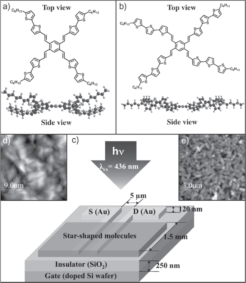
For device applications, thin films are the most suitable because of the availability of a wide range of materials and compatibility with practical device structure. However, such advantages have a trade-off relation with device performance. Cho et al achieved high values of R (2500–4300 A W−1) and P (4 × 10⁴) using 1,2,4,5-tetra(50-hexyl-[2, 20]-bithiophenyl-5-vinyl)-benzene (4(HPBT)-benzene) and 1,2,4,5-tetra(50-hexyl-[2, 20]terthiophenyl-5-vinyl)-benzene (4(HP3T)-benzene) [71]. Although these values are lower than those reported from single crystals, they are the best performance of thin-film organic phototransistors to date. Molecular structures, film morphologies, and device structures are shown in figure 9. The authors claimed that the closely packed film structures and the four-armed π-conjugation paths of the molecules played important roles on the high phototransistor performance. Pal et al produced a poly(3-hexylthiophene-2,5-diyl) (P3HT)-based phototransistor by a drop-casting technique, with R = 250 A W−1 and P = 3.8 × 10³ [72]. Of special note is the use of a solution process. Other thin-film-based phototransistors have been developed from 2,5-bis-biphenyl-4-yl-thieno[3,2-b]thiophene (BPTT) [73], titanyl phthalocyanine (TiOPc) [74], pentacene [75], and 2,7-bis-(N,N8-diphenylamino)-28,78-bis(biphenyl-4-yl)-9,98-spirobifluorene [76], with values of R from 1.3 to 82 A W−1.
Figure 9.
Molecular structures, film morphologies, and device structures of 4(HPBT)-benzene and 4(HP3T)-benzene phototransistors. Reprinted from [71] with permission; © 2008 Wiley-VCH, Weinheim, Germany.
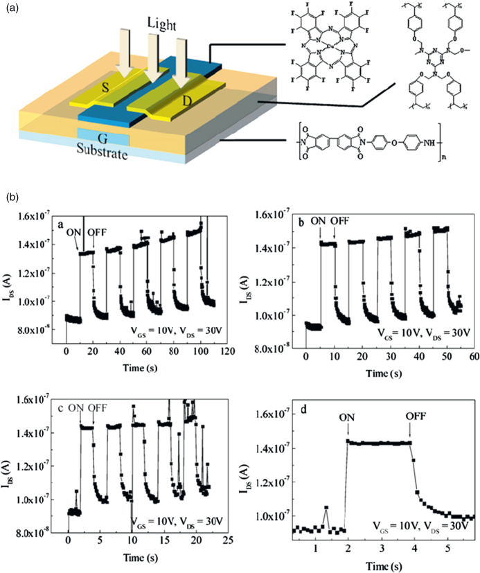
Pyo et al used fluorinated Cu-phthalocyanine (F16CuPc), which works as an n-type semiconductor, for the phototransistor channel. The R value was very low, around 1.5 mA W−1. However, a fast switching speed below 10 ms was achieved [77, 78]. In this study, a poly(4-phenoxy methylstyrene) (P4PMS) was employed as a gate insulating layer. The phenoxymethyl (-CH2OC6H5) group made the surface of P4PMS hydrophobic and prohibited the absorption of water to the dielectric. Furthermore, the dielectric had no OH groups that would act as a charge trapping site. These features of P4PMS improved switching speed. They produced a similar phototransistor with F16CuPc on a polyimide substrate to create a flexible phototransistor [79]; the device structure, molecular structures, and optical switching behaviors are shown in figure 10. They also fabricated a CMOS inverter from pentacene and F16CuPc that could control the threshold voltage from 28.6 V to 19.9 V upon illumination [80].
Figure 10.
(a) Device structure of phototransistor consisting of F16CuPc, cross-linked poly(4-vinyl phenol), and polyimide substrate. (b) Photoswitching behaviors under constant bias voltages. Reprinted from [79] with permission; © 2011 Elsevier BV.
Other distinct works to reduce operating voltage and to control threshold voltage have been reported. Salinas and Halik inserted a fullerene-attached self-assembled monolayer (C60-SAM) between a gate dielectric Al2O3 layer and transistor channel layers (pentacene and dihexylsexithiophene [DH6T]) [81]. The C60 works as an acceptor to reduce the operating voltage. Mok et al developed a phototransistor with a P3HT-TiO2 composite film [82]. The P3HT absorbs light to produce excitons, and the TiO2 enhances carrier dissociation by trapping electrons to increase the hole density in the P3HT. Such trapped carriers in turn effectively reduce the threshold voltage.
Yang et al have effectively utilized a helically shaped chiral molecule, helicene, for a photoresponsive OFET [83]. A feature of the device is that handedness, which is a unique character of chiral molecules, had been successfully applied for circularly polarized light-detection. They argued that new photonic technology, such as quantum-based optical computing and communication, would be realized by this device.
Nanowire phototransistors
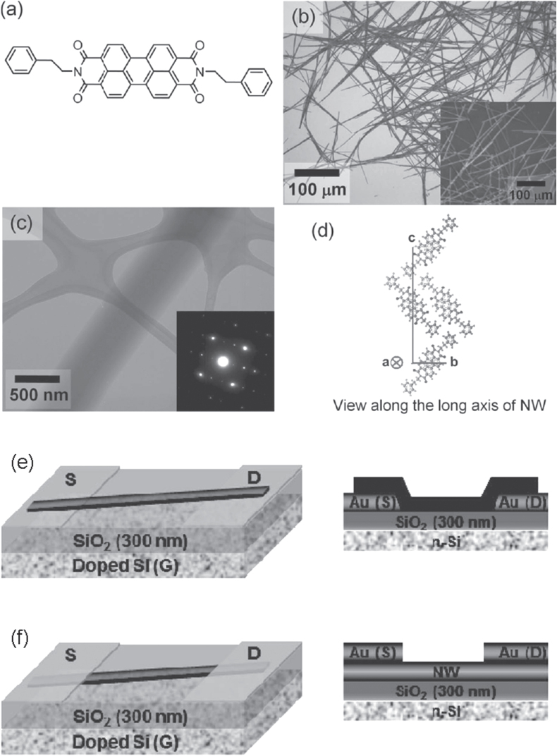
Recently, one-dimensional wire structures have attracted attention for phototransistors. The advantages of the nanowires are compatibility with flexible devices due to elongated dimension and improved carrier mobilities due to the single-crystal structure. The high surface-to-volume ratio is another merit for effective photon-carrier conversion. Hoang et al synthesized single-crystalline nanowires of π-extended porphyrin derivatives, ZnTP and H2TP, for transistor channels and achieved high performance: R = 2.2 × 10⁴ A W−1 and a carrier mobility of 2.90 cm2 Vs−1 for ZnTP [84]. The high performance of the FETs is mainly due to formation of J-aggregation of H-aggregated dimeric porphyrin pairs in the crystal structures, resulting in stronger intermolecular π–π interactions with short layer distances and enhancement of charge transport of photogenerated carriers. Yu et al developed a single-crystal nanowire phototransistor with n-type N,N′-bis(2-phenylethyl)-perylene-3,4:9,10-tetracarboxylic diimide (BPE-PTCDI) [85]; the molecular structure, microscope images of nanowires, and top- and bottom-contact device structures are shown in figure 11. The nanowires were grown along a-axis direction with the shortest π-planer distance of 3.4 Å, indicating that effective charge transport is attained along the long axis of the nanowire. The well-ordered molecular alignment achieved a high R of 1.40 × 10³ A W−1, P of 4.93 × 10³, and a mobility of 1.13 cm2 Vs−1 under an optimized wavelength of 532 nm. Excellent performance of nanowire transistors has also been achieved by using 1,3,6,8-tetrakis((4-hexyl phenyl)ethynyl)pyrene [86], highly aligned polymeric nanowires [87], and self-assembled 6,13-bis(methylthio)pentacene nanowires [88, 89].
Figure 11.
(a) Chemical structure; (b), (c) microscope images; (d) molecular packing of BPE-PTCDI nanowire ‘(NW)’. Device structures of (e) bottom- and (f) top-contact configuration. Reprinted from [85] with permission; © 2013 Wiley-VCH, Weinheim, Germany.
In spite of these advantages, there is a hurdle to be overcome. Most reported nanowires have been produced via ‘bottom-up’ self-assembly processes, but these processes do not permit precise device integration. Thus, to establish nanowire alignment techniques, ‘top-down’ techniques will be the next challenge for further development of nanowire phototransistors. The nano-imprinting technique is a promising candidate for this purpose because it enables production of well-ordered nanowire arrays [90, 91]. Furthermore, this technique improves chain alignments of π-conjugated polymers via the nano-confinement effect, which is advantageous for carrier transport [92, 93].
Photo-induced non-volatile memory
A variety of organic memory devices have been developed by using ferroelectric, conductive, and semiconducting polymers [94–96] in various device configurations, e.g., three-dimensional cross-bar structures [97, 98]. The cross-bar structure is advantageous owing to simplicity and high number density. Meanwhile, the three-terminal transistor structure offers promise for applications, in particular the effective use of light for multi-level memory operation. The basic device structure is a bottom-gate transistor, similar to that of phototransistors. The operation principle is based on photo-induced carrier generation in organic transistor channels and their trapping at the semiconductor–dielectric hetero-interface or in the dielectric layers. Thus, trapped carriers cause hysteresis in the transistor properties, i.e., variations in threshold voltage, to generate the memory function. The threshold voltage can be regulated by both pulse-gate voltage (write voltage) and light irradiation, which make multi-level memory possible.
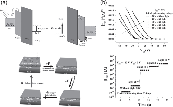
Guo et al first proposed a device consisting of pentacene or Cu-phthalocyanine for the channel layers and SiO2 layers with a polystyrene or poly(methyl methacrylate) (PMMA) surface coating for the dielectric layers [99]. A model of carrier transfer and trapping is illustrated in figure 12(a). Five-level memory operation was demonstrated by tuning light irradiation and gate voltage (figure 12(b)). They achieved a high operation speed of 1 μs and a long retention time of 250 h. Feng et al reported similar work, using a conjugated polymer, poly(9,9-dioctylfluorene), as a coating layer on SiO2 [100]. Barra et al developed the same memory device with n-type semiconducting N,N-dioctyl-3,4,9,10-perylene tetracarboxylic diimide (PTCDI-C8H) with a retention time of 20 days (480 h) [101], which is longer than those of the other organic memories such as flash memory and ferroelectric memory. These photo-assisted non-volatile memories have a potential for new applications, including flexible and disposable memory devices [18, 102, 103].
Figure 12.
(a) Energy-level diagrams to explain carrier transfer and trapping at the semiconductor–polymer interface, and illustrations of the possible mechanism of the charge generation and complexation. (b) Photo-induced variations in transistor properties and corresponding drain current levels. Reprinted from [99] with permission; © 2009 Wiley-VCH, Weinheim, Germany.
A critical issue of these memory devices is the high operating voltage of up to 200 V. Recent studies have been devoted to reducing the read and write voltages. Shang et al prepared a pentacene-based transistor with PMMA-coated Al2O3 film for the dielectric layer, with a dielectric constant (k) higher than that of SiO2 [91]. They achieved a four-level memory operation at read and write voltages lower than 10 V. The retention time was only 104 s, but read–write operation was repeatable more than 104 times. Liu et al used a similar approach (pentacene transistor on a high-k Ta2O5 film with a polymer surface coating) and achieved an operating voltage of 10–15 V and a retention time of 103–104 s [103, 104]. In these works, the operating voltage was reduced by using high-k inorganic films. In addition, Wang et al elucidated that polymeric insulating film can be used as a dielectric layer [105]. They attained a very low operating voltage of around 2 V with an ultrathin pinhole-free poly(methyl methacrylate co glycidyl methacrylate) film. Their device also works as a phototransistor with an R value of 1250 A W−1.
A strong point of organic optical memory devices is that multi-level memory is attainable by a combination of bias voltages and photo-induced carrier generation. This merit leads to high-speed operation on the order of microseconds. The next goal is to increase the number of carrier trapping sites to ensure controllable variations in the threshold voltage. This goal is critical also for large-scale integration of memory devices.
Photochromism in OFETs
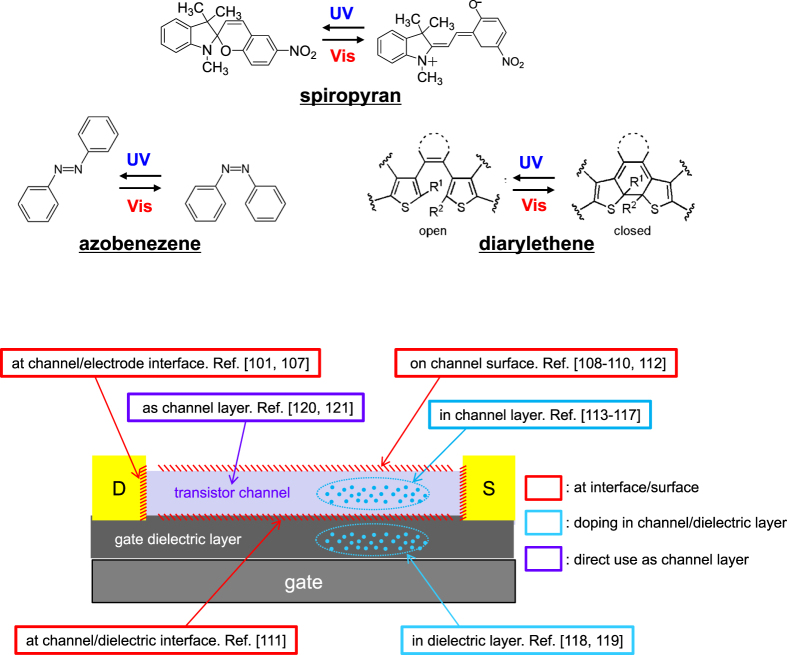
To be exact, the term of ‘photochromism’ represents only the reversible color variation involved in conformational change. However, this term is widely used to describe reversible changes in molecular conformations of organic compounds upon exposure to UV and visible light. Typical photochromism of this sort can be divided into three types: cis trans isomerization of azobenzene, non-ionic–ionic isomerization of spiropyran, and open–closed-ring isomerization of diarylethene (figure 13). These conformational changes accompany variations in physical properties, including energy levels, π-conjugation, color, and polarity. Because these photo-induced changes in physical properties can remain even after irradiation, photochromism is applicable to optical memory, switching, and sensing. A question is how we can incorporate the photochromism-originated phenomena into practical device structures. This section introduces a variety of attempts to modify transistor properties by incorporating photochromism into the OFET device configuration. As summarized in figure 13, these attempts can be categorized into three groups: interface/surface engineering, doping in channel/dielectric layers, and direct use of photochromic layers as channel layers.
Figure 13.
(a) Photochromic reactions of azobenzene, spiropyran, and diarylethene. (b) Photochromism in the organic transistor at interface/surface, in channel/dielectric layers, and as the channel layer.
Interface/surface engineering
Self-assembling monolayers with photochromic substituents have been used in OFETs. Zhang et al inserted spiropyran-SAMs at the interface of the electrode–pentacene channel [106]. Photo-induced dipole variation in spiropyran affected the carrier injection. As a result, they observed an on/off ratio of drain current (Ion/Ioff) of about 1.6. Crivillers et al reported a similar attempt [107]; an azobenzene-SAM at the electrode–N,N′-1H,1H-perfluorobutyl dicyanoperylenecarboxydiimide (PDIF-CN2) interface induced a variation in the carrier injection barrier to result in Ion/Ioff = 2.0. Additionally, azobenzene or spiropyran were attached to the surface of low-dimensional materials: graphene, carbon nanotubes, and polymer nanowires [108–110]. In these cases, photochromic molecules are near the carrier flow, and therefore photochromism can influence the drain current. Most notably, Bardavid et al achieved a high Ion/Ioff of 10 [109].
Yoshida et al inserted a diarylethene thin film at a pentacene channel–dielectric PMMA interface [111]. UV–visible light irradiation induced open–closed-ring isomerization in the diarylethene molecules. Carriers in the transistor channel were trapped or released by the corresponding reversible changes in the HOMO–LUMO levels. They reported Ion/Ioff = 5.0. Shen et al proposed a spiropyran layer on the surface of the pentacene channel [112]. However, the effect on spiropyran photochromism was very small (Ion/Ioff = 1.6), because most of the drain current runs just near the channel–dielectric interface.
Doping in channel/dielectric layers
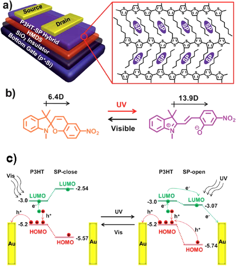
Photochromic molecules have been mixed into channel layers as dopants to modify the electrical current through the channels. These approaches can simplify fabrication process compared with the abovementioned interface/surface engineering. For example, Li et al used a spiropyran-doped P3HT film as a transistor channel [113]. The device structure and molecules are illustrated in figures 14(a) and (b). UV irradiation produced an open-ring spiropyran, which involves a reduction of the LUMO level. The lowered LUMO level enhanced electron transfer from the P3HT to the Au electrode (see energy diagram on the left of figure 14(c)). Even though the on/off ratio was very small (Ion/Ioff = 1.05), they demonstrated a repeatable photoswitching. Orgiu et al proposed a similar approach [114]; they doped diarylethene into a P3HT polymer layer. UV irradiation produced closed-ring isomers to raise the HOMO level, which can trap holes in the channel layer. The open-ring isomer has a lower HOMO level and has no impact on the drain current. In this manner, they realized optical switching of the drain current (Ion/Ioff = 5.0) through the P3HT channel. Raimondo et al doped Au nanoparticles, which were surrounded by azobenzene-SAMs, into P3HT [115]; the Au nanoparticles promoted the conformational change by a plasmon effect under irradiation.
Figure 14.
(a) Device structure with a spiropyran-doped P3HT channel layer. HMDS stands for hexamethyldisilazane. (b) Reversible conformational change of spiropyran (SP). (c) Energy-level diagrams to explain photo-induced carrier transfer between P3HT and drain electrode via spiropyran molecules. Reprinted from [113] with permission; © 2012, Royal Society of Chemistry, UK.
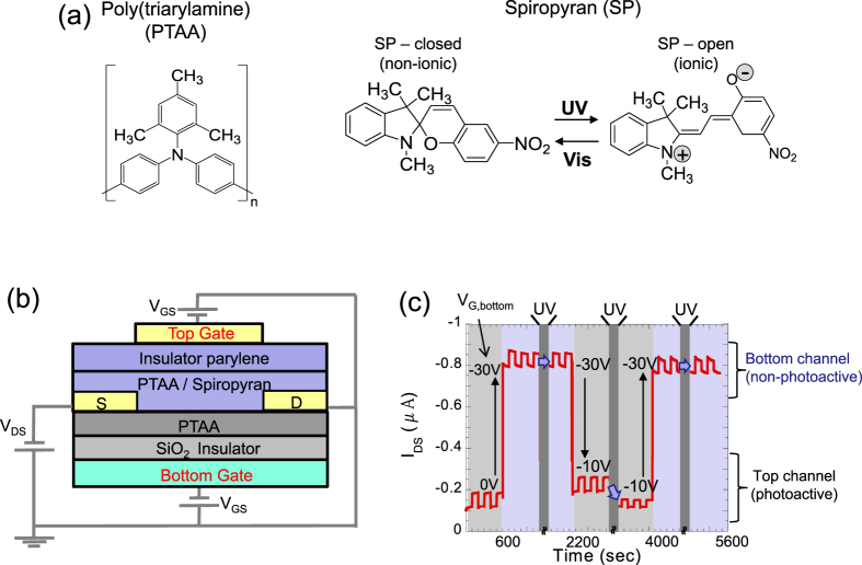
All these studies used P3HT as a host layer. P3HT forms crystalline thin films, and therefore the concentration of the dopant has an upper limit due to phase separation. To solve this problem, Ishiguro et al used poly[bis(4-phenyl) (2,4,6-trimethylphenyl)amine] (PTAA) as a channel layer, in which spiropyran was doped [116] (figure 15(a)). The amorphous structure of PTAA allows a high doping concentration of up to 70 wt%. They elucidated that the ionic polarized state of the open-ring spiropyran created scattering sites to disturb hole transport. From this fundamental work, they developed a multi-level optical switching device, in which doped and non-doped PTAA layers were stacked in a dual-gate transistor configuration [117]. The device structure and switching behavior are shown in figures 15(b) and (c).
Figure 15.
(a) Chemical structures of PTAA and spiropyran. (b) Device structure of a dual-gate transistor with spiropyran-doped and non-doped PTAA channels. (c) Photo-induced and gate bias-induced multi-level switching of drain current. Reprinted from [116] with permission; © 2013, Royal Society of Chemistry, UK.
Doping of photochromic molecules into polymeric dielectric layers is also effective to modify the transistor properties [118, 119]. The spiropyran molecules are dispersed in a PMMA dielectric layer. The photochromic reaction of spiropyran accompanies a reversible variation of the dipole moment, leading to photo-induced modification of the dielectric capacitance. An optical switching ratio of Ion/Ioff = 2.0 was reported.
Photochromic thin film as transistor channel
In the studies described above, photochromic molecules are ‘guests’ used to impose changes in the electrical current through the ‘host’ semiconducting channels. Recent studies, in contrast, have used photochromic molecules directly as transistor channels, aiming at improving the on/off ratios. Arlt et al used an azobenzene derivative for a channel layer, but the hole mobility and on/off ratio were still low: 9.8 × 10⁻⁶ cm2 Vs−1 and Ion/Ioff = 2.5 [120]. Hayakawa et al used a diarylethene molecule as the transistor channel to give a direct impact of photochromism on the drain current [121]. The photochromic change between open- and closed-ring diarylethene (figure 16(a)) is accompanied by a drastic change in π-conjugation. With this advantage, they achieved an extremely high on/off ratio of Ion/Ioff = 300 (figure 16(b)). To increase on-current, π-conjugation in open-rings should be enhanced. But, π-conjugation that is too great would hinder the photoisomerization and increase off-current. In this manner, appropriate molecular design will lead to further improvement of optical switching.
Figure 16.
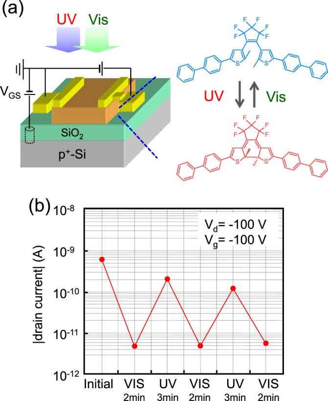
(a) Device structure and open-/closed-ring isomerization of diarylethene. (b) Photo-induced switching of drain current with high on/off ratio. Reprinted from [121] with permission; © 2013, American Chemical Society, USA.
Summary and perspectives
Since the first preparation of LE-OFET, various research approaches have enabled novel organic photonics applications using cost-effective manufacturing processes. For example, the development of LE-OFETs will lead to new display technologies, because LE-OFETs can merge OLEDs and OFETs into single devices. In addition, the expected improvements in light-emission efficiency and brightness of LE-OFETs, as well as their full compatibility with well-established electronic and photonic planar technologies, may allow the development of optical communication systems, integrated optoelectronic systems, and electrically pumped organic lasers. In contrast to LE-OFETs, LR-OFETs are still in the embryonic stage. Among them, phototransistors hold promise, because some of their parameters surpass those of conventional Si-based phototransistors. Durability needs to be improved. The reported performances of non-volatile memory and photochromic transistors are preliminary and require further efforts. However, these devices could open new frontiers for photonic and electronic devices, e.g., flexible, lightweight, high-density data storage or optical memory devices.
The device performance of both photoactive OFETs faces a number of issues. Firstly, the material design should be optimized to enhance carrier processes, such as transport, recombination, and emission/absorption of light. Secondly, deep investigation of the hetero-interfaces is required to improve the efficiency of these carrier processes. Thirdly, fine techniques of thin-film growth, either wet or dry, are necessary for precise fabrication of these hetero-interfaces. This is because the device performance can be improved by controlling the morphological and crystallographic features of the active materials at the different organic–organic, organic–metal, and organic–dielectric interfaces. Finally, further optimization of the device configurations is essential, although these developments may complicate the fabrication processes. To satisfy these requirements, interdisciplinary collaborations between organic chemists and device physicists are indispensable.
References
- Friend R H. Nature. 1999;397:121. doi: 10.1038/16393. [DOI] [Google Scholar]
- Spanggaard H. and Krebs F C. Sol. Energy Mater. Sol. Cells. 2004;83:125. doi: 10.1016/j.solmat.2004.02.021. [DOI] [Google Scholar]
- Lu G, Usta H, Risko C, Wang L, Facchetti A, Ratner M A. and Marks T J. J. Am. Chem. Soc. 2008;130:7670. doi: 10.1021/ja800424m. [DOI] [PubMed] [Google Scholar]
- Forrest S R. Nature. 2004;428:911. doi: 10.1038/nature02498. [DOI] [PubMed] [Google Scholar]
- Katz H E. Chem. Mater. 2004;16:4748. doi: 10.1021/cm049781j. [DOI] [Google Scholar]
- Lucas B, Trigauda T. and Videlot-Ackermann C. Polym. Int. 2012;61:374. doi: 10.1002/pi.3213. [DOI] [Google Scholar]
- Hasegawa T. and Takeya J. Sci. Technol. Adv. Mater. 2009;10:024202. doi: 10.1088/1468-6996/10/2/024314. [DOI] [PMC free article] [PubMed] [Google Scholar]
- Dimitrakopoulos C D. and Malenfant P R L. Adv. Mater. 2002;14:99. doi: 10.1002/(ISSN)1521-4095. [DOI] [Google Scholar]
- Heimel G, Salzmann I, Duhm S. and Koch N. Chem. Mater. 2011;23:359. doi: 10.1021/cm1021257. [DOI] [Google Scholar]
- Yamashita Y. Sci. Technol. Adv. Mater. 2009;10:024202. doi: 10.1088/1468-6996/10/2/024313. [DOI] [PMC free article] [PubMed] [Google Scholar]
- Witte G. and Wöll C. J. Mater. Res. 2004;19:1889. doi: 10.1557/JMR.2004.0251. [DOI] [Google Scholar]
- Kowarik S, Gerlach A. and Schreiber F. J. Phys.: Condens. Matter. 2008;20:024202. doi: 10.1088/0953-8984/20/18/184005. [DOI] [Google Scholar]
- Minemawari H, Yamada T, Matsui H, Tsutsumi J, Haas S, Chiba R, Kumai R. and Hasegawa T. Nature. 2011;475:364. doi: 10.1038/nature10313. [DOI] [PubMed] [Google Scholar]
- Nakayama K. Adv. Mater. 2011;23:1626. doi: 10.1002/adma.201004387. [DOI] [PubMed] [Google Scholar]
- Guo Y, Yu G. and Liu L. Adv. Mater. 2010;22:4427. doi: 10.1002/adma.v22:40. [DOI] [PubMed] [Google Scholar]
- Koopmans B, Wagemans W, Bloom F L, Bobbert P A, Kemerink M. and Wohlgenannt M. Phil. Trans. R. Soc. A. 2011;369:3602. doi: 10.1098/rsta.2011.0172. [DOI] [PubMed] [Google Scholar]
- Samuel I D W. and Turnbull G A. Chem. Rev. 2007;107:1272. doi: 10.1021/cr050152i. [DOI] [PubMed] [Google Scholar]
- Sekitani T, Yokota T, Zschieschan U, Klauk H, Bauer S, Takeuchi K, Takamiya M, Sakurai T. and Someya T. Science. 2009;326:1516. doi: 10.1126/science.1179963. [DOI] [PubMed] [Google Scholar]
- Yang G, Di C-A, Zhang G, Zhang J, Xiang J, Zhang D. and Zu D. Adv. Funct. Mater. 2013;23:1671. doi: 10.1002/adfm.v23.13. [DOI] [Google Scholar]
- Wu Y. ACS Appl. Mater. Interfaces. 2012;4:1883. doi: 10.1021/am3003389. [DOI] [PubMed] [Google Scholar]
- Naber W J M, Faez S. and van der Wiel W G. J. Phys. D: Appl. Phys. 2007;40:R205. doi: 10.1088/0022-3727/40/12/R01. [DOI] [Google Scholar]
- Hepp A, Heil H, Weise W, Ahles M, Schmechel R. and Seggern H V. Phys. Rev. Lett. 2003;91:024202. doi: 10.1103/PhysRevLett.91.157406. [DOI] [PubMed] [Google Scholar]
- Muccini M. Nat. Mater. 2006;5:605. doi: 10.1038/nmat1699. [DOI] [PubMed] [Google Scholar]
- Cicoira F. and Santato C. Adv. Funct. Mater. 2007;17:3421. doi: 10.1002/(ISSN)1616-3028. [DOI] [Google Scholar]
- Muccini M, Koopman W. and Toffanin S. Laser Photonics Rev. 2012;6:258. doi: 10.1002/lpor.201100008. [DOI] [Google Scholar]
- Santato C. Synth. Met. 2004;146:329. doi: 10.1016/j.synthmet.2004.08.028. [DOI] [Google Scholar]
- Santato C, Manunza I, Bonfiglio A, Cicoira F, Cosseddu P, Zamboni R. and Muccini M. Appl. Phys. Lett. 2005;86:024202. doi: 10.1063/1.1898429. [DOI] [Google Scholar]
- Oyamada T, Sasabe H, Adachi C, Okuyama S, Shimoji N. and Matsushige K. Appl. Phys. Lett. 2005;86:024202. doi: 10.1063/1.1870105. [DOI] [Google Scholar]
- Cicoira F, Santato C, Melucci M, Favaretto L, Gazzano M, Muccini M. and Barbarella G. Adv. Mater. 2006;18:169. doi: 10.1002/(ISSN)1521-4095. [DOI] [Google Scholar]
- Capelli R, Dinelli F, Loi M A, Murgia M, Zamboni R. and Muccini M. J. Phys.: Condens. Matter. 2006;18:024202. doi: 10.1088/0953-8984/18/33/S28. [DOI] [Google Scholar]
- Zaumseil J, Friend R H. and Sirringhaus H. Nat. Mater. 2006;5:69. doi: 10.1038/nmat1537. [DOI] [Google Scholar]
- Zaumseil J, McNeill C R, Bird M, Smith D L, Ruden P P, Roberts M, McKiernan M J, Friend R H. and Sirringhaus H. J. Appl. Phys. 2008;103:024202. doi: 10.1063/1.2894723. [DOI] [Google Scholar]
- Zaumseil J, Donley C L, Kim J-S, Friend R H. and Sirringhaus H. Adv. Mater. 2006;18:2708. doi: 10.1002/(ISSN)1521-4095. [DOI] [Google Scholar]
- Zaumseil J, Kline R J. and Sirringhaus H. Appl. Phys. Lett. 2008;92:024202. doi: 10.1063/1.2836790. [DOI] [Google Scholar]
- Naber R C G, Bird M. and Sirringhaus H. Appl. Phys. Lett. 2008;93:024202. doi: 10.1063/1.2957472. [DOI] [Google Scholar]
- Gwinner M C, Vaynzof Y, Banger K K, Ho P K H, Friend R H. and Sirringhaus H. Adv. Funct. Mater. 2010;20:3457. doi: 10.1002/adfm.v20:20. [DOI] [Google Scholar]
- Gwinner M C, Kabra D, Roberts M, Brenner T J K, Wallikewitz B H, McNeill C R, Friend R H. and Sirringhaus H. Adv. Mater. 2012;24:2728. doi: 10.1002/adma.v24.20. [DOI] [PubMed] [Google Scholar]
- Gwinner M C, Jakubka F, Gannott F, Sirringhaus H. and Zaumseil J. ACS Nano. 2012;6:539. doi: 10.1021/nn203874a. [DOI] [PubMed] [Google Scholar]
- Takahashi T, Takenobu T, Takeya J. and Iwasa Y. Adv. Funct. Mater. 2007;17:1623. doi: 10.1002/(ISSN)1616-3028. [DOI] [Google Scholar]
- Bisri S Z, Takenobu T, Yomogida Y, Shimotani H, Yamao T, Hotta S. and Iwase Y. Adv. Funct. Mater. 2009;19:1728. doi: 10.1002/adfm.v19:11. [DOI] [Google Scholar]
- Bisri S Z, Takenobu T, Sawabe K, Tsuda S, Yomogida Y, Yamao T, Hotta S, Adachi C. and Iwase Y. Adv. Mater. 2011;23:2753. doi: 10.1002/adma.201004572. [DOI] [PubMed] [Google Scholar]
- Nakanotani H, Saito M, Nakamura H. and Adachi C. Adv. Funct. Mater. 2010;20:1610. doi: 10.1002/adfm.v20:10. [DOI] [Google Scholar]
- Nakanotani H, Saito M, Nakamura H. and Adachi C. Appl. Phys. Lett. 2009;95:024202. doi: 10.1063/1.3216047. [DOI] [Google Scholar]
- Rost C, Karg S, Riess W, Loi M A, Murgia M. and Muccini M. Appl. Phys. Lett. 2004;85:1613. doi: 10.1063/1.1785290. [DOI] [Google Scholar]
- Loi M A, Rost-Bietsch C, Murgia M, Karg S, Riess W. and Muccini M. Adv. Funct. Mater. 2006;16:41. doi: 10.1002/(ISSN)1616-3028. [DOI] [Google Scholar]
- Dinelli F, Capelli R, Loi M A, Muccini M, Facchetti A. and Marks T J. Adv. Mater. 2006;18:1416. doi: 10.1002/(ISSN)1521-4095. [DOI] [Google Scholar]
- Di C, Yu G, Liu Y, Xu X, Wei D, Song Y, Sun Y, Wang Y. and Zhu D. Adv. Funct. Mater. 2007;17:1567. doi: 10.1002/(ISSN)1616-3028. [DOI] [Google Scholar]
- Seo H-S, Zhang Y, An M-J. and Choi J-H. Org. Electron. 2009;10:1293. doi: 10.1016/j.orgel.2009.07.009. [DOI] [Google Scholar]
- Seo H-S, An M-J, Zhang Y. and Choi J-H. J. Phys. Chem. C. 2010;114:6141. doi: 10.1021/jp9114699. [DOI] [Google Scholar]
- Zhang Y, Seo H-S, An M-J, Oh J-D. and Choi J-H. J. Appl. Phys. 2011;109:024202. doi: 10.1063/1.3573537. [DOI] [Google Scholar]
- Seo H-S, Kim D-K, Oh J-D, Shin E-S. and Choi J-H. J. Phys. Chem. C. 2013;117:4764. doi: 10.1021/jp311816t. [DOI] [Google Scholar]
- Capelli R, Toffanin S, Geberali G, Usta H, Facchetti A. and Muccini M. Nat. Mater. 2010;9:496. doi: 10.1038/nmat2751. [DOI] [PubMed] [Google Scholar]
- Mathushima T. and Adachi C. Appl. Phys. Lett. 2006;89:024202. doi: 10.1063/1.2410236. [DOI] [Google Scholar]
- Toffanin S, Capelli R, Koopman W, Geberali G, Cavallini S, Stefani A, Saguatti D, Ruani G. and Muccini M. Laser Photonics Rev. 2013;7:1011. doi: 10.1002/lpor.201300066. [DOI] [Google Scholar]
- Seo J H, Namdas E B, Gutacker A, Heeger A J. and Bazan G C. Adv. Funct. Mater. 2011;21:3667. doi: 10.1002/adfm.201100682. [DOI] [Google Scholar]
- Swensen J S, Soci C. and Heeger A J. Appl. Phys. Lett. 2005;87:024202. doi: 10.1063/1.2149986. [DOI] [Google Scholar]
- Swensen J S, Yuen J, Gargas D, Buratto S K. and Heeger A J. J Appl. Phys. 2007;102:024202. doi: 10.1063/1.2752582. [DOI] [Google Scholar]
- Namdas E B, Ledochowitsch P, Yuen J D, Moses D. and Heeger A J. Appl. Phys. Lett. 2008;92:024202. doi: 10.1063/1.2920436. [DOI] [Google Scholar]
- Seo J H, Namdas E B, Gutacker A, Heeger A J. and Bazan G C. Appl. Phys. Lett. 2010;97:024202. doi: 10.1063/1.3467856. [DOI] [Google Scholar]
- Hsu B B Y. ACS Nano. 2013;7:2344. doi: 10.1021/nn305566u. [DOI] [PubMed] [Google Scholar]
- Xu Z, Li S H, Ma L, Li G. and Yang Y. Appl. Phys. Lett. 2007;91:024202. doi: 10.1002/adma.200800601. [DOI] [Google Scholar]
- Liu B, McCarthy M A, Yoon Y, Kim D Y, Wu Z, So F, Holloway P H, Reynolds J R, Guo J. and Rinzler A G. Adv. Mater. 2008;20:3605. doi: 10.1002/adma.v20:19. [DOI] [Google Scholar]
- McCarthy M A, Liu B, Donoghue E P, Kravchenko I, Kim D Y, So F. and Rinzler A G. Science. 2011;332:570. doi: 10.1126/science.1203052. [DOI] [PubMed] [Google Scholar]
- Jung M H, Choi I, Chung H-J. and Kim O. Jpn J. Appl. Phys. 2008;47:8275. doi: 10.1143/JJAP.47.8275. [DOI] [Google Scholar]
- Hsu B B Y, Duan C, Namdas E B, Gutacker A, Yuen J D, Huang F, Cao Y, Bazan G C, Samuel I D W. and Heeger A J. Adv. Mater. 2012;24:1171. doi: 10.1002/adma.v24.9. [DOI] [PubMed] [Google Scholar]
- Liu J, Engquist I. and Berggren M. J. Am. Chem. Soc. 2013;135:024202. doi: 10.1021/ja308200f. [DOI] [PubMed] [Google Scholar]
- Kim K H. Adv. Mater. 2011;23:3095. doi: 10.1002/adma.v23.27. [DOI] [PubMed] [Google Scholar]
- Mukherjee B, Sim K, Shin T J, Lee J, Mukherjee M, Ree M. and Pyo S. J. Mater. Chem. 2012;22:3192. doi: 10.1039/c2jm14179e. [DOI] [Google Scholar]
- Jiang H, Yang X, Cui Z, Liu Y, Li H. and Hu W. Appl. Phys. Lett. 2009;94:024202 [Google Scholar]
- Mukherjee B, Mukherjee M, Sim K. and Pyo S. J. Mater. Chem. 2011;21:1931. doi: 10.1039/c0jm02513e. [DOI] [Google Scholar]
- Cho M Y, Kim S J, Han Y D, Park D H, Kim K H, Choi D H. and Joo J. Adv. Funct. Mater. 2008;18:2905. doi: 10.1002/adfm.v18:19. [DOI] [Google Scholar]
- Pal T, Arif M. and Khondaker S I. Nanotechnology. 2010;21:024202. doi: 10.1088/0957-4484/21/32/325201. [DOI] [PubMed] [Google Scholar]
- Noh Y-Y, Kim D-Y, Yoshida Y, Yase K, Jung B-J, Lim E. and Shim H-K. Appl. Phys. Lett. 2005;86:024202. doi: 10.1063/1.1856144. [DOI] [Google Scholar]
- Ji Z, Shang L, Lu C, Wang L, Guo J, Wang H, Li D. and Liu M. IEEE Electron Device Lett. 2012;33:1619. doi: 10.1109/LED.2012.2212412. [DOI] [Google Scholar]
- Hu Y, Dong G, Liu C, Wang L. and Qiu Y. Appl. Phys. Lett. 2006;89:024202. doi: 10.1063/1.2336722. [DOI] [Google Scholar]
- Saragi T P I, Pudzich R, Fuhrmann T. and Salbeck J. Appl. Phys. Lett. 2004;84:2334. doi: 10.1063/1.1690110. [DOI] [Google Scholar]
- Mukherjee B, Mukherjee M, Choi Y. and Pyo S. J. Phys. Chem. C. 2009;113:024202. doi: 10.1021/jp906102r. [DOI] [Google Scholar]
- Mukherjee B, Mukherjee M, Choi Y. and Pyo S. ACS Appl. Mater. Interfaces. 2010;2:1614. doi: 10.1021/am100127q. [DOI] [PubMed] [Google Scholar]
- Park J, Mukherjee B, Cho H, Kim S. and Pyo S. Synth. Met. 2011;161:143. doi: 10.1016/j.synthmet.2010.11.010. [DOI] [Google Scholar]
- Kim S, Lim T, Sim K, Kim H, Choi Y, Park K. and Pyo S. ACS Appl. Mater. Interfaces. 2011;3:1451. doi: 10.1021/am101284m. [DOI] [PubMed] [Google Scholar]
- Salinas M. and Halik M. Appl. Phys. Lett. 2013;102:024202. doi: 10.1063/1.4804595. [DOI] [Google Scholar]
- Mok S M, Yan F. and Chan H L W. Appl. Phys. Lett. 2008;93:024202. doi: 10.1063/1.2957981. [DOI] [Google Scholar]
- Yang Y, Correa da Costa R, Fuchter M J. and Campbell A J. Nature Photonics. 2013;7:634. doi: 10.1038/nphoton.2013.176. [DOI] [Google Scholar]
- Hoang M H, Kim Y, Kim M, Kim K H, Lee T W, Nguyen D N, Kim S J, Lee K, Lee S J. and Choi D H. Adv. Mater. 2012;24:5363. doi: 10.1002/adma.201202148. [DOI] [PubMed] [Google Scholar]
- Yu H, Bao Z. and Oh J H. Adv. Funct. Mater. 2013;23:629. doi: 10.1002/adfm.201201848. [DOI] [Google Scholar]
- Kim Y S. Chem. Commun. 2011;47:8907. doi: 10.1039/c1cc11589h. [DOI] [PubMed] [Google Scholar]
- Liu Y, Dong H, Jiang S, Zhao G, Shi Q, Tan J, Jiang L, Hu W. and Zhan X. Chem. Mater. 2013;25:2649. doi: 10.1002/adma.201203792. [DOI] [Google Scholar]
- Wakayama Y, Hayakawa R, Chikyow T, Machida S, Nakayama T, Egger S, de Oteyza D G, Dosch H. and Kobayashi K. Nano Lett. 2008;8:3273. doi: 10.1021/nl801649v. [DOI] [PubMed] [Google Scholar]
- Wakayama Y, Hiroshiba N, Hayakawa R, Chikyow T. and Kobayashi K. Jpn J. Appl. Phys. 2012;51:024202. doi: 10.7567/JJAP.51.06FA01. [DOI] [Google Scholar]
- Chen Y. and Luo Y. Adv. Mater. 2009;21:2040. doi: 10.1002/adma.v21:20. [DOI] [Google Scholar]
- Huang C, Dong B, Lu N, Yang B, Gao L, Tian L, Qi D, Wu Q. and Chi L. Small. 2009;5:583. doi: 10.1002/smll.v5:5. [DOI] [PubMed] [Google Scholar]
- Aryal M, Trivedi K. and Hu W. ACS Nano. 2009;3:3085. doi: 10.1021/nn900831m. [DOI] [PubMed] [Google Scholar]
- Zheng Z, Yim K-H, Saifullah M S M, Welland M E, Friend R H, Kim J-S. and Huck W T S. Nano Lett. 2007;7:987. doi: 10.1021/nl070022k. [DOI] [PubMed] [Google Scholar]
- Ling Q-D, Liaw D-J, Zhu C, Chan D S-H, Kang E-T. and Neoh K-G. Prog. Polym. Sci. 2008;33:917. doi: 10.1016/j.progpolymsci.2008.08.001. [DOI] [Google Scholar]
- Nabe R C G, Asadi K, Blom P W M, de Leeuw D M. and de Boer B. Adv. Mater. 2010;22:933. doi: 10.1002/adma.200900759. [DOI] [PubMed] [Google Scholar]
- Heremans P, Gelinck G H, Muller R, Baeg K-J, Kim D-Y. and Noh Y-Y. Chem. Mater. 2011;23:341. doi: 10.1021/cm102006v. [DOI] [Google Scholar]
- Paul S. IEEE Trans. Nanotechnol. 2007;6:191. doi: 10.1109/TNANO.2007.891824. [DOI] [PMC free article] [PubMed] [Google Scholar]
- Song S, Cho B, Kim T-W, Ji Y, Jo M, Wang G, Choe M, Kahng Y H, Hwang H. and Lee T. Adv. Mater. 2010;22:5048. doi: 10.1002/adma.v22.44. [DOI] [PubMed] [Google Scholar]
- Guo Y, Di C, Ye S, Sun X, Zheng J, Wen Y, Wu W, Yu G. and Liu Y. Adv. Mater. 2009;21:1954. doi: 10.1002/adma.v21:19. [DOI] [Google Scholar]
- Feng C, Mei T, Huc X. and Pavel N. Org. Electron. 2010;11:1713. doi: 10.1016/j.orgel.2010.07.024. [DOI] [Google Scholar]
- Barra M, Cassinese F B A, Girolamo F V D. and Vicari L. J. Appl. Phys. 2009;106:024202. doi: 10.1063/1.3272035. [DOI] [Google Scholar]
- Shang L, Ji Z, Wang H, Chen Y, Liu X, Han M. and Liu M. IEEE Electron Device Lett. 2011;32:1451. doi: 10.1109/LED.2011.2162218. [DOI] [Google Scholar]
- Liu X, Dong G, Duan L, Wang L. and Qiu Y. J. Mater. Chem. 2012;22:024202. doi: 10.1039/c2jm15747k. [DOI] [Google Scholar]
- Liu X, Dong G, Zhao D, Wang Y, Duan L, Wang L. and Qiu Y. Org. Electron. 2012;13:2917. doi: 10.1016/j.orgel.2012.08.024. [DOI] [Google Scholar]
- Wang W, Ma D. and Gao Q. IEEE Electron Device Lett. 2012;59:1510. doi: 10.1109/TED.2012.2187296. [DOI] [Google Scholar]
- Zhang H, Guo X, Hui J, Hu S, Xu W. and Zhu D. Nano Lett. 2011;11:4939. doi: 10.1021/nl2028798. [DOI] [PubMed] [Google Scholar]
- Crivillers N, Orgiu E, Reinders F, Mayor M. and Samorì P. Adv. Mater. 2011;23:1447. doi: 10.1002/adma.201003736. [DOI] [PubMed] [Google Scholar]
- Kim M, Safron N S, Huang C, Arnold M S. and Gopalan P. Nano Lett. 2012;12:182. doi: 10.1021/nl2032734. [DOI] [PubMed] [Google Scholar]
- Guo X, Huang L, O’Brien S, Kim P. and Nuckolls C. J. Am. Chem. Soc. 2005;127:024202. doi: 10.1021/ja054335y. [DOI] [PubMed] [Google Scholar]
- Bardavid Y, Goykhman I, Nozaki D, Cuniberti G. and Yitzchaik S. J. Phys. Chem. C. 2011;115:3123. doi: 10.1021/jp110665j. [DOI] [Google Scholar]
- Yoshida M, Suemori K, Uemura S, Hoshino S, Takada N, Kodzasa T. and Kamata T. Jpn J. Appl. Phys. 2010;49:024202 [Google Scholar]
- Shen Q, Cao Y, Liu S, Steigerwald M L. and Guo X. J. Phys. Chem. C. 2009;113:024202. doi: 10.1021/jp9026817. [DOI] [Google Scholar]
- Li Y, Zhang H, Qi C. and Guo X. J. Mater. Chem. 2012;22:4261. doi: 10.1039/c1jm14872a. [DOI] [Google Scholar]
- Orgiu E. Nat. Chem. 2012;4:675. doi: 10.1038/nchem.1384. [DOI] [PubMed] [Google Scholar]
- Raimondo C, Crivillers N, Reinders F, Sander F, Mayor M. and Samorì P. Proc. Natl Acad. Sci. USA. 2012;109:024202. doi: 10.1073/pnas.1203848109. [DOI] [PMC free article] [PubMed] [Google Scholar]
- Ishiguro Y, Hayakawa R, Chikyow T. and Wakayama Y. J. Mater. Chem. C. 2013;1:3012. doi: 10.1039/c3tc30130c. [DOI] [Google Scholar]
- Ishiguro Y, Hayakawa R, Yasuda T, Chikyow T. and Wakayama Y. ACS Appl. Mater. Interfaces. 2013;5:9726. doi: 10.1021/am402833k. [DOI] [PubMed] [Google Scholar]
- Shen Q, Wang L, Liu S, Cao Y, Gan L, Guo X, Steigerwald M L, Shuai Z, Liu Z. and Nuckolls C. Adv. Mater. 2010;22:3282. doi: 10.1002/adma.201000471. [DOI] [PubMed] [Google Scholar]
- Lutsyk P, Janus K. and Sworakowski J. J. Phys. Chem. C. 2011;115:3106. doi: 10.1021/jp108982x. [DOI] [Google Scholar]
- Arlt M, Scheffler A, Suske I, Eschner M, Saragi T P I, Salbeck J. and Fuhrmann-Lieker T. Phys. Chem. Chem. Phys. 2010;12:024202. doi: 10.1039/c0cp00643b. [DOI] [PubMed] [Google Scholar]
- Hayakawa R, Higashiguchi K, Matsuda K, Chikyow T. and Wakayama Y. ACS Appl. Mater. Interfaces. 2013;5:3625. doi: 10.1021/am400030z. [DOI] [PubMed] [Google Scholar]


