Abstract
12CaO·7Al2O3 electride, a sub-nanoporous compound having a work function of 2.4 eV, was examined as a candidate cathode material in fluorescent lamps. The electron emission yield was higher and the discharge voltage was lower for 12CaO·7Al2O3 than for existing cathode materials such as Ni, Mo or W; therefore, the energy consumption of the fluorescent lamps can be improved using 12CaO·7Al2O3 cathodes. Prototype glow-discharge lamps using 12CaO·7Al2O3 were constructed and exhibited reasonable durability.
Keywords: C12A7 electride, nanoporous material, cathode material, electron emission, fluorescent lamp
Introduction
Cold-cathode fluorescent lamps (CCFLs) [1] have been widely used for light-emitting devices, such as backlight for the liquid crystal display or general lighting. Although light-emitting diodes (LEDs) are being used for these purposes [2], CCFLs still have several advantages such as large-area illumination and low cost. However, the luminous efficacy of CCFLs is limited mainly by the discharge properties of the cathode electrode. In a practical fluorescent lamp, visible light is generated by the phosphor, which is excited by the UV light emitted from mercury in the noble-gas discharge plasma [3]. The electron emission properties of the cathode material are closely related to the energy consumption, driving voltage and luminous efficiency of the lamp [4], since the behavior of the discharge plasma is mainly controlled via the surface of the cathode. Metals such as Ni, Mo or W have been generally used as cathode materials for fluorescent lamps.
12CaO·7Al2O3 (C12A7) electride [5–10] is a new electronic oxide compound with a work function as low as 2.4 eV [11–13], which is close to those of alkaline metals. Its crystal structure can be regarded as a stack of cage-like subunits [14, 15] that share their faces, and this arrangement differs from that of zeolite-based compounds [16–20]. The inner diameter of the cage is approximately 0.4 nm. A part of these cages can clathrate an electron as depicted in figure 1. Owing to the mobility of these cage electrons, C12A7 exhibits a high electrical conductivity of up to 1500 S cm−1, and the low work function of this electride originates from the midgap states created by these electrons [21–25]. The operating voltage of the fluorescence lamp is known to be closely related to the work function of the cathode material, and the work function is much smaller for C12A7 (2.4 eV) than for Ni (5.0 eV), Mo (4.6 eV) or W (4.5 eV). Therefore, in this study, the C12A7 electride was evaluated as a candidate cathode material in a CCFL. We examined the electron emission and discharge voltage of this material by fabricating glow-discharge lamps with a C12A7 cold cathode and tested their endurance for up to 1000 h.
Figure 1.
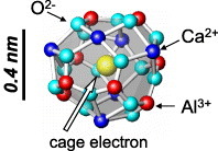
Cage structure of the C12A7 electride.
Cathode material for CCFL
The top part of figure 2 shows the mechanism of CCFL [1]. The discharge is initiated by applying a voltage between the two electrodes, which is called the firing voltage. One of the conditions for the firing is that the electron density exceeds 1010−1011 cm−3 at the discharge space inside the tube. The electrons are supplied by the cathode electrode via the secondary electron emission excited by the noble gas ions at the cathode surface. Once the discharge is started, the discharge plasma becomes electrically conductive and it is possible to maintain the discharge at a lower voltage than the firing voltage; this voltage is called the sustaining voltage. The visible light is emitted by the phosphor that is excited by the UV light emitted by mercury in the discharge plasma.
Figure 2.
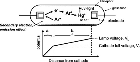
Schematic of the CCFL operation (top) and the distribution of electrical potential within the CCFL (bottom).
The lower part of figure 2 shows the electrical potential within the lamp. The drop near the cathode in region a is called the cathode fall voltage; it is closely related to the electron emission properties of the cathode materials. The voltage drop of region b occurs in the body of the discharge plasma called the positive column. The sustaining voltage is the sum of the cathode fall voltage and the positive column fall voltage. The latter is determined primarily by the nature of the plasma such as the gas pressure or the ionization energy of the discharge gas. Although the energy consumption at the cathode fall region a is indispensable for sustaining the discharge, it does not directly contribute to the light emission.
Several materials have been studied to reduce the cathode fall voltage, thereby improving the luminous efficiency of CCFLs [26–29]. For example, it has been known that the luminous efficiency is improved by changing the cathode material from Ni to Mo, as a result of the reduction in the cathode fall voltage. Improvement was also achieved by depositing a film of doped diamond or MgO on the surface of a metal electrode, thereby lowering the electron emission threshold [30–39], although the lifetime of the lamp was not satisfactory.
Ion-induced secondary electron emission from C12A7
Secondary electron emission
In secondary electron emission, the electrons are produced by bombarding solid surfaces with electrons, ions or neutral particles. In this study, the electron emission was induced by the positive ions via the γ effect and is called ion-induced secondary electron emission. The irradiating ion loses its energy while penetrating the surface of the cathode. A part of this energy is transferred to the electrons in the solid, which move toward the surface, and those electrons having an energy exceeding the work function of the material are emitted from the surface. Therefore, the emission intensity mostly depends on the ion species, work function, kinetic energy of electrons and the incident angle of the ions. It is evaluated with the secondary electron emission coefficient, γ, which is the number of electrons emitted per incoming particle.
Ion-induced secondary electron emission is classified into kinetic emission and potential emission [40, 41], which are dominated by the kinetic energy and ionization potentials (ionization voltage) of the incident ions, respectively. In the case of the potential emission, the secondary electrons are emitted through Auger neutralization by the positive ion that reaches a solid surface, whereas the kinetic emission is induced by the nuclear collisions between the incident ions and the solid. To drive a discharge lamp at a low voltage, it is more important for the discharge cathode to have a good potential emission property than kinetic emission property, because potential emission can be induced by less energetic ions. In fluorescent lamps, secondary electron emission is less studied for excitation with negative than with positive ions.
The potential emission has been evaluated with the following qualitative index [42, 43]:
Here, U is the ionization potential of the incident ion and ϕ is the work function. The potential emission proceeds if the above condition is met, and γ increases with increasing value of the left part of this inequality. Condition (1) might also be applied to the emission from deep levels in a semiconductor or an insulator by substituting the specific energy levels for the work function.
However, it is difficult to predict the value of γ from the above inequality, because γ is also affected by such processes as penetration of incident ions, energy transfer from the ions to electrons in the solid, diffusion of electrons to the surface and electrochemical reactions at the surface, among others. The cathode fall voltage is known to be closely related to γ, which was treated theoretically in references [39, 44] and evaluated experimentally in this study, using the C12A7 electride.
Measurement of the ion-induced secondary electron emission coefficient
Figure 3 shows the setup used for measuring γ in this study [32–35, 45–49]. It consists of a vacuum chamber, an ion gun and an electrode to collect the emitted electrons. The sample is irradiated with various ion beams using an ion gun. The emitted electrons are detected by the collector electrode placed near the sample surface. To collect the emitted electrons, the collector electrode is biased positively (collector voltage) with respect to the sample. The value of γ was calculated as
where IC is the collector current and IS is the sample current.
Figure 3.
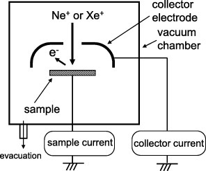
Measurement of the ion-induced secondary electron emission coefficient γ.
Polycrystalline bulk samples of C12A7 were prepared using carbon or aluminum as a reducing agent to control the cage electron densities [50–54]. The electron densities were measured as 3.0×10¹⁹ and 1.4×1021 cm−3, respectively, by electron spin resonance and diffuse reflectance spectroscopy. The samples for the measurements were prepared as follows. Polycrystalline powder of 12CaO·7Al2O3 was synthesized from a stoichiometric mixture of CaCO3 and Al2O3 powders, in a solid-state reaction carried out at 1300 °C for 6 h in air. The 12CaO·7Al2O3 powder was pressed into disks and annealed at 1350 °C for 3 h in air. One disk was then placed in an Al2O3 container, with Al powder that served as the reducing reagent, and annealed at 1300 °C for 10 h in a vacuum furnace. Another disk was melted in a carbon crucible at 1600 °C for 5 h and cooled at a rate of 400 °C h−1 to room temperature, in order to obtain material with a moderate cage electron density. The sample surfaces were abraded with a diamond file before measurements, which were performed in a vacuum of 10−5 Pa. Ion-induced secondary electron emission was measured by irradiating the samples, at normal incidence, with Ne+ or Xe+ ions accelerated by a voltage ranging between 100 and 600 V. The ionization potentials of Ne and Xe are 21.6 and 12.1 eV, respectively.
Figure 4(a) shows the dependence of γ on the collector voltage measured at an acceleration voltage of 600 V for the sample with an electron density of N=1021 cm−3. At low or negative collector voltages, γ is small owing to the presence of emitted electrons that are not captured by the collector electrode. The dependence of γ on the collector voltage is caused by the distribution of the kinetic energy of emitted electrons, which depends on the electronic structure near the surface or the surface potential induced by the ion irradiation. Figure 4(b) shows the energy distribution of the emitted electrons, which is the derivative of γ versus the collector voltage. The distribution is centered at approximately 5 eV for the N=1021 cm−3 sample; this value is typically below 5 eV for the metal and often more than 10 eV for the insulator.
Figure 4.
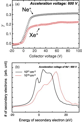
(a) γ versus collector voltage for the sample with an electron density of N=1021 cm−3. (b) Energy distribution of the emitted electrons for Ne+ excitation of samples with electron densities of 1019 and 1021 cm−3.
Figure 5 shows the dependence of γ on the acceleration voltage of the incident ions measured at a collector voltage of 80 V. The γ value for Ne+ ions (γNe) accelerated at 600 V was 0.31, which is close to that of W (γ=0.25, work function 4.5 eV) measured at the same acceleration voltage [55]. On the other hand, the γXe value was 0.17–0.22, an order of magnitude larger than the value of 0.02 for W. Whereas the γNe values were comparable for electron densities of N=1019 and 1021 cm−3, γXe increased with electron density from 0.17 to 0.22 at an acceleration voltage of 600 V. γXe slightly depended on the ion acceleration voltage, particularly for low voltages, showing that γXe is mainly dominated by the potential emission rather than the kinetic emission. The dependence on the incident ion energy was not apparent in the case of γNe. However, γNe was larger than γXe at any acceleration voltage, indicating that γNe is dominated by potential emission, since the ionization potential is higher for Ne (21.6 eV) than for Xe (12.1 eV).
Figure 5.
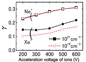
γ versus acceleration voltage of the incident ions for samples with electron densities of 1019 and 1021 cm−3.
The above observations can be explained as follows. Figure 6 schematically illustrates the electronic structure of the C12A7 electride [8–13, 21–25]. The vertical axis indicates the energy measured from the vacuum level and the horizontal axis corresponds to the density of states. As shown in the figure, the secondary electron emission proceeds through at least two stages: (i) energy transfer from the incident ion to the electrons in the solid by Auger neutralization and (ii) emission of the electrons having the energy exceeding the work function from the surface of the material. The ionization potential of Xe is 12.1 eV and the work function of C12A7 is only 2.4 eV. Therefore, the cage electrons in C12A7 receive sufficient energy from the Xe+ ions to be emitted, as described using equation (1). On the other hand, the energy of the valence band top (sum of the band gap energy and electron affinity) is approximately 7.9 eV. Thus, the valence electrons do not meet the energy requirement for emission. The efficiency of the excitation of the cage electrons by Xe+ ions increases with increasing electron density (density of states in the band corresponding to cage electrons), which explains the observed dependence of γ on the cage electron density. The ionization potential of Ne is 21.6 eV. This energy is sufficiently high to excite either cage electrons or valence band electrons, explaining the weak dependence of γ on the cage electron density.
Figure 6.
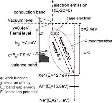
Electronic structure of the C12A7 electride.
C12A7 electride as a cathode material for CCFLs
Measurement of discharge properties with an open-cell apparatus
The discharge properties of C12A7 electride were studied using the apparatus shown in figure 7(a) [30, 36, 56]. It is possible to evaluate the discharge characteristics of the cathode material, under various pressures of discharge gas, without fabricating a lamp based on that material. Moreover, it is possible to measure exclusively the cathode fall voltage of the cathode material, by choosing a flat plate of the cathode and a cathode–anode distance small enough to eliminate the positive column.
Figure 7.
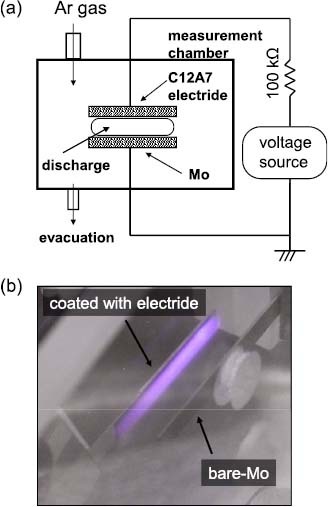
(a) Schematic of the open-cell discharge experiment. (b) A film of C12A7 electride used as a cathode.
The open-cell discharge experiments were performed on a film of C12A7 electride deposited on a Mo substrate by the paste coating technique. The film had an area of 5×10 mm2, a thickness of 20 μm and an electron density of approximately 1020 cm−3. A bare Mo substrate was placed as the counterelectrode and was used alternately as the cathode for referencing the cathode fall voltage. The distance between the two electrodes was maintained at 2.8 mm by glass spacers. Since the cathode fall voltage is markedly affected by the gas impurities, this arrangement allows the comparison of cathode materials under the same atmosphere. After the samples were placed in the measurement chamber, it was evacuated to 10−5 Pa and the discharge gas was introduced into it; the gas pressure was varied during the measurements. Ar was chosen as the discharge gas because it is commonly used for fluorescent lamps. A sinusoidal voltage was applied between the two samples at a frequency of 10 Hz to drive them as a cold cathode.
Figure 7(b) shows a photograph of the samples during the glow discharge, and the parameters of the driving voltage are summarized in figure 8(a). Figure 8(b) shows the cathode fall voltage and the firing voltage observed for the Mo and C12A7 electride. The discharge current was set between 1 and 10 mA, which is a typical current density for CCFLs. In this current range, the cathode fall voltage was almost constant at a fixed gas pressure despite the change in the discharge current, confirming that the cathode is operated in the normal glow regime. As shown in figure 8(b), the firing voltage and cathode fall voltage were lower for C12A7 than for Mo at any gas pressure.
Figure 8.
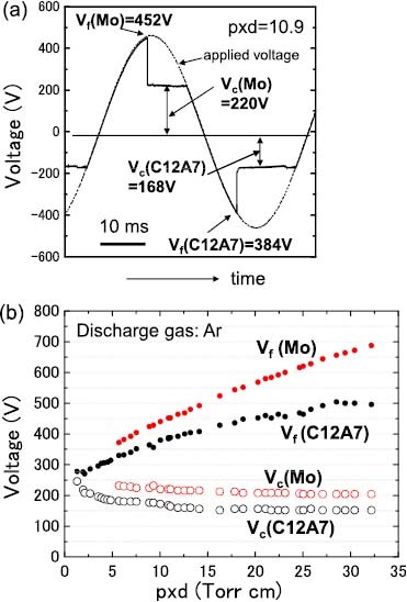
(a) Driving parameters of Mo and C12A7 electride film including firing voltage (Vf) and cathode fall voltage (Vc). (b) Measured dependences of Vf and Vc on the gas pressure (p).
Discharge properties of the cold-cathode lamp using C12A7 electride
Cold-cathode glow-discharge lamps were fabricated using the C12A7 electride to investigate its discharge properties. A sintered polycrystalline body of C12A7 was processed into a cylinder with a hollow 5 mm in diameter and 5 mm in depth. The processed sample was placed in a carbon container with a lid and kept at 1300 °C for 10 h under nitrogen atmosphere. The resulting sample had an electron density of 1020 cm−3 and was used as a cathode for the lamp, as shown in figure 9. The hollow shape of the cathode is often used in CCFLs because it results in a more efficient use of the exciting ions and photoelectrons and decreases the discharge voltage as compared with the flat cathode. These properties result from the confinement of the discharge plasma to the inner hollow and the enlargement of the surface area that acts as a cathode and are called the hollow effect in the lamp industry [57]. The discharge gas of the fabricated lamp was pure Ar kept at a pressure of 5 Torr and the glass tube had no phosphor. Ni was used as the anode and the distance between the cathode and anode was set at 1 cm. For comparison, we assembled a lamp with a cathode made of Mo instead of C12A7. Although Ni is widely used as the CCFL cathode material, metal Mo was chosen as a reference because it exhibits the lowest discharge voltage among the practical CCFL cathode materials.
Figure 9.
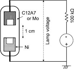
Structure of the fabricated lamps and the measurement circuit.
The lamps were fabricated as follows. First, the evacuated lamp tube with all the electrodes was annealed at 400 °C to remove the adsorbed gas species. After the lamp was cooled to room temperature, it was filled with the discharge gas and sealed. As shown in figure 9, the fabricated lamps were driven by dc voltage, with a 100 kΩ resistor connected in series.
Figure 10(a) shows a lamp operating with the C12A7 cathode and its current–voltage curve is plotted in figure 10(c). The lamp went off when the current was lower than the minimum value shown in figure 10, and the negative glow overflowed the hollow cathode when the current exceeded the maximum value. A lower lamp voltage was observed for a C12A7 than a Mo cathode and the minimum voltage to maintain the glow discharge (minimum discharge sustaining voltage) was 110 V. The lamp voltage is considered to be almost the same as the cathode fall voltage in this experiment because of the short distance between the discharge electrodes and because no positive column was observed during the discharge. Thus, the lowest cathode fall voltage can be assumed as 110 V for the C12A7 cathode, whereas it was deduced as 170 V for the Mo cathode lamp. The firing voltage was measured by applying a pulsed voltage at a frequency of 10 Hz, and the obtained values were 310 and 336 V for C12A7 and Mo, respectively. The discharge current was higher for C12A7 than for Mo at a given applied voltage. For comparison, the same lamp was filled with Xe instead of Ar and its discharge is shown in figure 10(b). Figure 10(d) presents the corresponding I–V curves revealing that the use of C12A7 reduced the cathode fall voltage for Xe as well as for Ar. Table 1 summarizes the discharge parameters of the C12A7 and Mo cathodes. In comparison with the results for parallel plates in vacuum, the fabricated lamps exhibited lower cathode fall voltage owing to the hollow effect.
Figure 10.
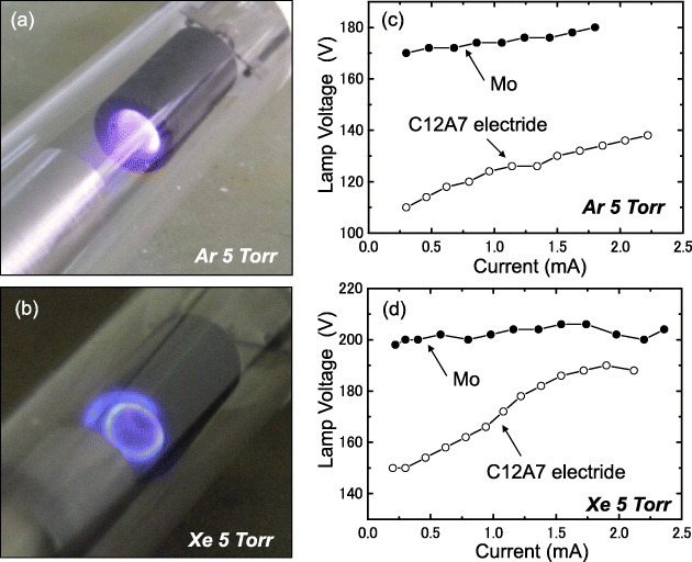
Lamps operating with a C12A7 hollow cathode in Ar (a) or Xe (b) gas and the corresponding I–V curves in Ar (c) or Xe(d).
Table 1.
Discharge properties of C12A7 and Mo.
| Gas | Cathode | Vf | min Vc |
|---|---|---|---|
| Ar | Molybdenum | 336 V | 170 V |
| C12A7 electride | 310 V | 110 V | |
| Xe | Molybdenum | 440 V | 198 V |
| C12A7 electride | 342 V | 150 V |
Vf: Firing voltage. min Vc: cathode fall voltage (minimum).
Stability to the discharge plasma is important for the cathode material of a fluorescent lamp, including resistance to sputtering and chemical stability to mercury used for ultraviolet emission. An endurance test was performed for a lamp operating with a C12A7 cathode and a mixture of Ar and Hg as the discharge gas, as shown in figure 11(a). The experimental setup was the same as that shown in figure 9. The current was regulated within the range of 1.0–1.1 mA by manually adjusting the dc voltage. The time traces of the discharge parameters shown in figure 11(b) reveal some fluctuations in the lamp voltage. In this Hg-containing lamp, the lamp voltage is dominated by the Hg content in the discharge gas because excitation of Hg requires an additional electric field. It is difficult to distinguish the cathode condition from the effect caused by the vapor pressure of Hg. However, it is noteworthy that the lamp voltage is stable within 20 V and did not increase even after 1000 h. In addition, no significant degradation in the brightness of the light emission from Hg or sputter deposits inside the glass tube was observed.
Figure 11.
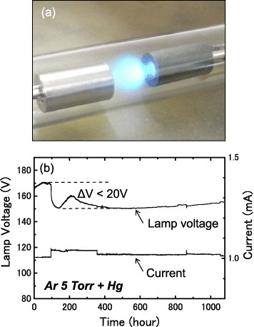
(a) Discharge in a C12A7 cathode lamp used for the endurance test. (b) Time traces of the lamp voltage and current.
Conclusions
The feasibility of the C12A7 electride as the cathode material for CCFLs was examined by fabricating prototype lamps and studying their ion-induced secondary electron emission. The cathode fall voltage, which is closely related to the energy consumption and luminous efficacy, was lower by approximately 35% in Ar and by 24% in Xe for a C12A7 cathode than for a Mo cathode. The use of C12A7 also allowed to reduce the firing voltage.
The endurance test was performed for 1000 h on a C12A7 cathode lamp filled with a mixture of Ar and Hg gases and showed that C12A7 is resistant to the discharge plasma. We found that not only bulk C12A7 but also thick C12A7 films exhibited low cathode fall and firing voltages. The secondary electron emission coefficient was measured as 0.22 for C12A7 irradiated by Xe+ ions, which is one order of magnitude larger than that of W. Xe is currently not used as the discharge gas for CCFLs because of the poor discharge properties. However, our results demonstrate that, using a C12A7 cathode, it is feasible to use Xe instead of Hg as the source of ultraviolet light for exciting the phosphor.
Acknowledgment
The authors are grateful to Professor Hiroshi Kajiyama of the Graduate School of Advanced Sciences of Matter, Hiroshima University, Japan, for discussions on the secondary electron emission.
References
- Yamaguchi K. LCD Backlights, In: Kobayashi S, Mikoshiba S, Lim S, editors. New York Wiley; 2009. p. p 91. [Google Scholar]
- Anandan M. J. Soc. Inf. Disp. 2008;16:287. doi: 10.1889/1.2841864. [DOI] [Google Scholar]
- Noguchi H. and Yano H. SID Symp. Dig. 2000;31:935. doi: 10.1889/1.1833109. [DOI] [Google Scholar]
- Hilscher A. J. Phys. D: Appl. Phys. 2002;35:1707. doi: 10.1088/0022-3727/35/14/311. [DOI] [Google Scholar]
- Dye J L. and DeBacker M G. Annu. Rev. Phys. Chem. 1987;38:271. doi: 10.1146/annurev.pc.38.100187.001415. [DOI] [Google Scholar]
- Dye J L. Science. 1990;247:663. doi: 10.1126/science.247.4943.663. [DOI] [PubMed] [Google Scholar]
- Dye J L. Inorg. Chem. 1997;36:3816. doi: 10.1021/ic970551z. [DOI] [Google Scholar]
- Hayashi K, Matsuishi S, Kamiya T, Hirano M. and Hosono H. Nature. 2002;419:462. doi: 10.1038/nature01053. [DOI] [PubMed] [Google Scholar]
- Dye J L. Science. 2003;301:607. doi: 10.1126/science.1088103. [DOI] [PubMed] [Google Scholar]
- Matsuishi S, Miyakawa M, Hayashi K, Kamiya T, Hirano M, Tanaka I. and Hosono H. Science. 2003;301:626. doi: 10.1126/science.1083842. [DOI] [PubMed] [Google Scholar]
- Toda Y, Matsuishi S, Hayashi K, Ueda K, Kamiya T, Hirano M. and Hosono H. Adv. Mater. 2004;16:685. doi: 10.1002/(ISSN)1521-4095. [DOI] [Google Scholar]
- Toda Y, Kim S W, Hayashi K, Hirano M, Kamiya T. and Hosono H. Appl. Phys. Lett. 2005;87:254103. doi: 10.1063/1.2149989. [DOI] [Google Scholar]
- Toda Y, Yanagi H, Ikenaga E, Kim J J, Kobata M, Ueda S, Kamiya T, Hirano M, Kobayashi K. and Hosono H. Adv. Mater. 2007;19:3564. doi: 10.1002/(ISSN)1521-4095. [DOI] [Google Scholar]
- Bartl H. and Scheller T. N. Jb. Miner. Mh. 1970;12:547. [Google Scholar]
- Imlach J A, Glasser L S D. and Glasser F P. Cement Concr. Res. 1971;1:57. doi: 10.1016/0008-8846(71)90083-4. [DOI] [Google Scholar]
- Barrer R M. and Cole J F. J. Phys. Chem. Solids. 1968;29:1755. doi: 10.1016/0022-3697(68)90159-5. [DOI] [Google Scholar]
- Kodaira T, Nozue Y, Ohwashi S, Goto T. and Terasaki O. Phys. Rev. 1993;48(B):12245. doi: 10.1103/PhysRevB.48.12245. [DOI] [PubMed] [Google Scholar]
- Srdanov V I, Stucky G D, Lippmaa E. and Engelhardt G. Phys. Rev. Lett. 1998;80:2449. doi: 10.1103/PhysRevLett.80.2449. [DOI] [Google Scholar]
- Petkov V, Billinge S J L, Vogt T, Ichimura A S. and Dye J L. Phys. Rev. Lett. 2002;89:075502. doi: 10.1103/PhysRevLett.89.075502. [DOI] [PubMed] [Google Scholar]
- Ichimura A S, Dye J L, Camblor M A. and Villaescusa L A. J. Am. Chem. Soc. 2002;124:1170. doi: 10.1021/ja016554z. [DOI] [PubMed] [Google Scholar]
- Sushko P V, Shluger A L, Hayashi K, Hirano M. and Hosono H. Phys. Rev. Lett. 2003;91:126401. doi: 10.1103/PhysRevLett.91.126401. [DOI] [PubMed] [Google Scholar]
- Sushko P V, Shluger A L, Hayashi K, Hirano M. and Hosono H. Thin Solid Films. 2003;445:161. doi: 10.1016/S0040-6090(03)01156-8. [DOI] [Google Scholar]
- Li Z, Yang J, Hou J G. and Zhu Q. Angew. Chem., Int. Ed. Engl. 2004;43:6479. doi: 10.1002/(ISSN)1521-3773. [DOI] [PubMed] [Google Scholar]
- Sushko P V, Shluger A L, Hirano M. and Hosono H. J. Am. Chem. Soc. 2007;129:942. doi: 10.1021/ja066177w. [DOI] [PubMed] [Google Scholar]
- Medvedeva J E, Teasley E N. and Hoffman M D. Phys. Rev. 2007;76(B):155107. doi: 10.1103/PhysRevB.76.155107. [DOI] [Google Scholar]
- Noguchi H. SID Symp. Dig. 1998;29:243. doi: 10.1889/1.1833738. [DOI] [Google Scholar]
- Ono T, Sakai T, Sakuma N, Suzuki M, Yoshida H. and Uchikoga S. Diam. Relat. Mater. 2006;15:1998. doi: 10.1016/j.diamond.2006.06.012. [DOI] [Google Scholar]
- Sakai T, Ono T, Sakuma N, Suzuki M. and Yoshida H. New Diam. Front. Carbon Technol. 2007;17:189. [Google Scholar]
- Lee J W, Jung S H, Lee M K, Jung S J, Song H S, Choi E H. and Cho G. SID Symp. Dig. 2009;40:1434. doi: 10.1889/1.3256576. [DOI] [Google Scholar]
- Bachmann P K, van Elsbergen, Wiechert D U, Zhong G. and Robertson J. Diam. Relat. Mater. 2001;10:809. doi: 10.1016/S0925-9635(01)00377-6. [DOI] [Google Scholar]
- Matsunaga Y, Kato T, Hatori T. and Hashiguchi S. J. Appl. Phys. 2003;93:5043. doi: 10.1063/1.1567034. [DOI] [Google Scholar]
- Ternyak O, Cheifetz E, Shchemelinin S, Breskin A, Chechik R, Zhang H, Avigal I. and Hoffman A. Diam. Relat. Mater. 2007;16:861. doi: 10.1016/j.diamond.2006.11.082. [DOI] [Google Scholar]
- Uchiike H, Miura K, Nakayama N, Shinoda T. and Fukushima Y. IEEE Trans. Electron Devices. 1976;23:1211. doi: 10.1109/T-ED.1976.18581. [DOI] [Google Scholar]
- Chou N J. J. Vac. Sci. Technol. 1977;14:307. doi: 10.1116/1.569148. [DOI] [Google Scholar]
- Moon K S, Lee J. and Whang K-W. J. Appl. Phys. 1999;86:4049. doi: 10.1063/1.371328. [DOI] [Google Scholar]
- Auday G, Guillot Ph. and Galy J. J. Appl. Phys. 2000;88:4871. doi: 10.1063/1.1290461. [DOI] [Google Scholar]
- Vink T J, Balkenende A R, Verbeek R G F A, van Hal H A M. and de Zwart S T. Appl. Phys. Lett. 2002;80:2216. doi: 10.1063/1.1464229. [DOI] [Google Scholar]
- Lim J Y, Oh J S, Ko B D, Cho J W, Kang S O, Cho G, Uhm H S. and Choi E H. J. Appl. Phys. 2003;94:764. doi: 10.1063/1.1581376. [DOI] [Google Scholar]
- Motoyama Y, Hirano Y, Ishii K, Murakami Y. and Sato F. J. Appl. Phys. 2004;95:8419. doi: 10.1063/1.1751239. [DOI] [Google Scholar]
- Hagstrum H D. Phys. Rev. 1954;96:336. doi: 10.1103/PhysRev.96.336. [DOI] [Google Scholar]
- Hagstrum H D. Phys. Rev. 1961;122:83. doi: 10.1103/PhysRev.122.83. [DOI] [Google Scholar]
- Motoyama Y, Ushirozawa M, Matsuzaki H, Takano Y. and Seki M. Bull. Am. Phys. Soc. 1999;44:52. [Google Scholar]
- Motoyama Y, Matsuzaki H. and Murakami H. IEEE Trans. Electron Devices. 2001;48:1568. doi: 10.1109/16.936562. [DOI] [Google Scholar]
- Kishinevsky L M. Radiat. Eff. 1973;19:23. doi: 10.1080/00337577308232211. [DOI] [Google Scholar]
- Choi E H, Oh H J, Kim Y G, Ko J J, Lim J Y, Kim J G, Kim D I, Cho G. and Kang S O. Japan. J. Appl. Phys. 1998;37:7015. doi: 10.1143/JJAP.37.7015. [DOI] [Google Scholar]
- Kalish R, Richter V, Cheifetz E, Zalman A. and Yona P. Appl. Phys. Lett. 1998;73:46. doi: 10.1063/1.121718. [DOI] [Google Scholar]
- Ishimoto M, Hidaka S, Betsui K. and Shinoda T. SID Symp. Dig. 1999;30:552. doi: 10.1889/1.1834081. [DOI] [Google Scholar]
- Choi E H, Lim J Y, Kim Y G, Ko J J, Kim D I, Lee C W. and Cho G S. J. Appl. Phys. 1999;86:6525. doi: 10.1063/1.371618. [DOI] [Google Scholar]
- Kim D I, Lim J Y, Kim Y G, Ko J J, Lee C W, Cho G S. and Choi E H. Japan. J. Appl. Phys. 2000;39:1890. doi: 10.1143/JJAP.39.1890. [DOI] [Google Scholar]
- Kim S W, Matsuishi S, Nomura T, Kubota Y, Takata M, Hayashi K, Kamiya T. and Hosono H. Nano Lett. 2007;7:1138. doi: 10.1021/nl062717b. [DOI] [PubMed] [Google Scholar]
- Kim S W, Miyakawa M, Hayashi K, Sakai T, Hirano M. and Hosono H. J. Am. Chem. Soc. 2005;127:1370. doi: 10.1021/ja043990n. [DOI] [PubMed] [Google Scholar]
- Kim S W, Toda Y, Hayashi K, Hirano M. and Hosono H. Chem. Mater. 2006;18:1938. doi: 10.1021/cm052367e. [DOI] [Google Scholar]
- Kim S W, Matsuishi S, Miyakawa M, Hayashi K, Hirano M. and Hosono H. J. Mater. Sci., Mater. Electron. 2007;18:5. doi: 10.1007/s10854-007-9183-y. [DOI] [Google Scholar]
- Matsuishi S, Kim S W, Kamiya T, Hirano M. and Hosono H. J. Phys. Chem. 2008;(C):112 4753. [Google Scholar]
- Hagstrum H D. Phys. Rev. 1954;96:325. doi: 10.1103/PhysRev.96.325. [DOI] [Google Scholar]
- van Elsbergen, Bachmann P K. and Juestel T. SID Symp. Dig. 2000;31:220. doi: 10.1889/1.1832922. [DOI] [Google Scholar]
- Alberts I L, Barratt D S. and Ray A K. J. Disp. Technol. 2010;6:52. doi: 10.1109/JDT.2009.2031924. [DOI] [Google Scholar]


