Abstract
Silicon waveguide optical non-reciprocal devices based on the magneto-optical effect are reviewed. The non-reciprocal phase shift caused by the first-order magneto-optical effect is effective in realizing optical non-reciprocal devices in silicon waveguide platforms. In a silicon-on-insulator waveguide, the low refractive index of the buried oxide layer enhances the magneto-optical phase shift, which reduces the device footprints. A surface activated direct bonding technique was developed to integrate a magneto-optical garnet crystal on the silicon waveguides. A silicon waveguide optical isolator based on the magneto-optical phase shift was demonstrated with an optical isolation of 30 dB and insertion loss of 13 dB at a wavelength of 1548 nm. Furthermore, a four port optical circulator was demonstrated with maximum isolations of 15.3 and 9.3 dB in cross and bar ports, respectively, at a wavelength of 1531 nm.
Keywords: Magneto-optical garnet, Direct bonding, Optical isolator, Optical circulator, Phase shift
Introduction
Optical isolators allow light waves to propagate in specified directions while preventing the propagation in undesired directions. Because of this behavior, the optical isolator is essential for protecting optical active devices from reflected light [1]. In addition, an optical circulator is an important component for realizing highly functional photonic circuits. Current optical isolators and circulators comprise of bulk optics and employ the magneto-optical Faraday effect, in which a polarization plane rotates in different directions depending upon the light propagation direction [2–4].
The same magneto-optical polarization rotation principle can be applied to waveguide non-reciprocal devices [5–9]. However, phase matching in the waveguide between the transverse electric (TE) and transverse magnetic (TM) modes must be realized in order to obtain the polarization rotation, i.e. TE–TM mode conversion. This can be achieved by balancing the various contributions to birefringence, e.g. geometrical, stress-induced and growth-induced birefringence [10]. Although it is possible, in principle, to control the various contributions to birefringence, the tolerances in the manufacturing process cause great difficulties in achieving the required control. In addition, the operation wavelength range is limited because the phase matching condition is sensitive to the wavelength. An isolator based on the magneto-optical phase shift has a distinct advantage over mode conversion: the TE–TM mode phase matching is not required when an isolator is used [11].
Magneto-optical effects are important for obtaining optical non-reciprocal functions. For optical fiber communication wavelength ranges, magneto-optical garnet crystals are commonly used owing to their large first-order magneto-optical effects and low optical absorption in practical applications [12]. However, it is very difficult to grow garnet crystals on the commonly used optical waveguide platforms such as silicon. We had previously developed a surface activated direct bonding technique to integrate a magneto-optical garnet on silicon and III–V compound semiconductors [13, 14]. Using this technique, a silicon waveguide optical isolator was fabricated for the first time with an optical isolation of 21 dB at a wavelength of 1559 nm [15]. The isolator employed a magneto-optical phase shift in a Mach–Zehnder interferometer (MZI). In addition, a GaInAsP waveguide optical isolator based on the MZI was fabricated with an isolation of 28 dB at 1550 nm wavelength [16]. In both isolators, a cerium-substituted yttrium iron garnet was directly bonded as an upper cladding layer on semiconductor guiding layers.
In addition to the magneto-optical phase shift, novel approaches are investigated for optical non-reciprocal functions. Yu et al [17] proposed a non-magneto-optical configuration using the electro-optic modulation in a silicon waveguide. A unidirectional mode conversion can be realized by modulating the light wave with a traveling RF wave. The fundamental guided mode traveling along the RF wave is converted to a higher order mode, the frequency of which is shifted by the frequency of the RF wave. The frequency that shifted toward the higher order mode is then selectively filtered out. Thus, the light wave is prohibited from propagating in that direction. Optical nonlinearity can be utilized to realize non-reciprocal transmittance. Fan et al [18] demonstrated an optical diode function in a silicon double ring resonator configuration. These non-magneto-optical approaches are advantageous as a magneto-optical material is not required to be integrated on a silicon waveguide. However, it is worth noting that an RF wave with a very high driving power is required for the traveling wave modulation device. In addition, optical diodes based on optical nonlinearity do not function as optical isolators when both forward and backward propagating light waves exist.
In this paper, we review the magneto-optical non-reciprocal devices developed for silicon photonics applications. In section 2, the preparation of magneto-optical garnet on silicon is discussed with a particular focus on the deposition and bonding techniques. The magneto-optical phase shift is useful to realize optical non-reciprocal devices in silicon waveguide platforms. Optical isolators based on the MZI and ring resonator are discussed in sections 3 and 4, respectively, while an MZI based optical circulator is described in section 5.
Magneto-optical material
Optical non-reciprocity can be obtained using magneto-optical effects. Integrating a magneto-optical material onto silicon is required for optical non-reciprocal devices on silicon waveguide platforms. Two approaches have been investigated: the deposition and bonding of magneto-optical materials. Since magneto-optical garnets have large first-order magneto-optical effects with low optical absorption, they are the best candidate for the optical non-reciprocal device applications in near infrared regions, such as the region between 1300 and 1550 nm. Hereafter, we limit our discussion to the garnet as a magneto-optical material for this application.
Deposition of magneto-optical material
Epitaxial growth of a magneto-optical garnet on silicon is challenging because of the large mismatch in physical properties between the garnet and silicon. For example, the lattice constant of yttrium iron garnet Y3Fe5O12 (YIG), which is the most popular magneto-optical garnet, is 1.238 nm, whereas that of silicon is 0.543 nm. Furthermore, the linear thermal expansion coefficients of YIG and silicon are 10.4 × 10⁻⁶ and 2.33 × 10⁻⁶ K−1, respectively.
Although a single-crystalline magneto-optical garnet has not been grown on silicon, progress in the deposition of magneto-optical garnets has been made. Stadler et al demonstrated the deposition of YIG poly-crystalline thin films on MgO and quartz substrates through a novel reactive sputtering method with rapid thermal annealing [19, 20]. Körner et al [21] deposited a poly-crystalline Bi3Fe5O12 layer through pulsed laser deposition (PLD) on SiO2 with an annealed YIG buffer layer.
Bi et al [22] demonstrated the growth of a magneto-optical garnet on silicon through PLD. They first deposited a 20 nm-thick YIG seed layer on an oxidized silicon substrate at 550 °C. The deposited layer was subjected to rapid thermal annealing at 850 °C for achieving crystallization in the YIG phase. Subsequently, bismuth-substituted YIG (Bi1.8Y1.2)Fe5O12 (Bi:YIG) or cerium-substituted YIG (Ce1Y2)Fe5O12 (Ce:YIG) was deposited on the YIG seed layer through PLD at 650 °C. The grown Bi:YIG and Ce:YIG layer showed poly-crystalline garnet phases with saturation Faraday rotations of −838 and −830° cm−1, respectively, at a wavelength of 1550 nm.
It is desirable to prepare magneto-optical garnets on silicon using deposition techniques from the viewpoint of the device fabrication process. The Faraday rotation available in the magneto-optical garnet prepared by deposition is much less than that of an epitaxially grown single-crystalline garnet, i.e. −830° cm−1 in PLD Ce:YIG [22] and −4500° cm−1 in sputter-epitaxially grown Ce:YIG [23] at a wavelength of 1550 nm. However, in order to reduce the required magneto-optical interaction length, a greater improvement in the Faraday rotation of the deposited garnet layer is required.
Surface activated direct bonding
Compared to the deposition techniques, bonding techniques are advantageous because single-crystalline layers that are epitaxially grown in a separate process can be used. When integrating a magneto-optical garnet with other materials for optical waveguide applications, a tight, uniform contact between the materials is required for obtaining a sufficient interaction between the light waves and magneto-optical garnet. A surface activated direct bonding technique is a powerful tool to realize a tight contact between dissimilar crystals [24–26]. We developed a surface activated direct bonding technique for integrating a magneto-optical garnet on a silicon waveguide [14]. The surfaces of the target wafers are activated in a vacuum chamber. Subsequently, the activated surfaces are brought into contact at room temperature. While applying a constant pressure, the contacted sample is annealed to obtain firm bonding.
There are several ways to achieve surface activation; they include argon ion beam and argon plasma irradiation. We found that exposing wafers to oxygen or nitrogen plasma was effective for a wafer combination of silicon and magneto-optical garnet. The surface smoothness is an important factor for successful bonding. We examined the effects of pre-cleaning and surface activation processes on the roughness of the wafer surfaces [13]. A 500 nm-thick cerium-substituted yttrium iron garnet (YCe)3Fe5O12 (Ce:YIG) single-crystalline layer was grown on a (111)-oriented substituted gadolinium gallium garnet (GdCa)3(GaMgZr)5O12 (SGGG) substrate through a sputter epitaxial growth technique. A (100)-oriented SOI wafer, in which the silicon layer was 220 nm thick, was used for examining the effects of pre-cleaning and surface activation processes on the roughness of the wafer surfaces. The details of pre-cleaning processes are described in [13].
Oxygen, nitrogen or argon gas was supplied at a flow rate of 100 sccm to a plasma reactor chamber with a pressure of 120 Pa. To generate the plasma, an RF power of 400 W at 13.56 MHz was applied to an electrode of 4 inch diameter. Ce:YIG and SOI wafers were cut into 20 × 20 mm2 pieces and placed on the electrode. The roughness of the wafer surfaces was measured using an atomic force microscope (AFM). The surface roughness, which is defined by the average of rms values obtained in the AFM measurement, is shown in figure 1 as a function of the plasma irradiation time. The measurement was performed on three areas of each wafer. As shown in figure 1, compared with the initial pre-cleaned state, the oxygen plasma irradiation reduces the surface roughness of both Ce:YIG and SOI for irradiation times between 10 and 30 s. In the case of nitrogen plasma irradiation, slight increases occurred in the surface roughness of both Ce:YIG and SOI for irradiation times <30 s. In contrast, the argon plasma irradiation increases the surface roughness of Ce:YIG monotonically with the increase in irradiation time. From these observations, it can be concluded that an oxygen or nitrogen plasma irradiation between 10 and 30 s is suitable for reducing the roughness of Ce:YIG and SOI surfaces.
Figure 1.
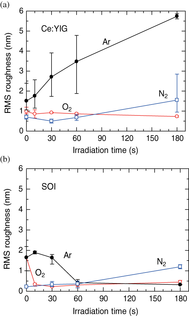
Measured surface roughness of (a) Ce:YIG and (b) SOI as a function of argon, oxygen and nitrogen plasma irradiation times.
After the surface activation process through the oxygen plasma irradiation for 30 and 10 s, respectively, for Ce:YIG and SOI, the wafers were brought into contact inside a vacuum chamber. The wafers were pressed together with a pressure of 5 MPa for 8 h. During this process, the sample was annealed at 200 and 250 °C for Ce:YIG and SOI, respectively. The Ce:YIG–SOI bonding was successfully achieved. The bonding strength measured through a tensile test was <0.02 MPa for the sample activated with oxygen plasma using an RF power of 400 W.
The bonding strength was improved to >1.8 MPa by exposing the wafers to oxygen plasma generated using a higher RF power of 500 W [13]. Such a high bonding strength can be attributed to the increase in surface activation energy. There was no remarkable degradation in the surface roughness of the wafers after the plasma irradiation generated using an RF power of 500 W. In addition, a bonding strength of 5.3 MPa was obtained by applying the surface activation process of nitrogen plasma generated with an RF power of 500 W for 10 s. In this process, the annealing was performed at 200 °C at a pressure of 6 MPa for 30 min.
MZI isolator
A magneto-optical isolator based on an MZI is discussed in this section. The isolator uses the phase shift induced by the magneto-optical effect [27]. The MZI optical isolator is advantageous as it operates in a single polarization mode. Thus, there is no need for the TE–TM mode phase matching.
The authors’ group measured the magneto-optical phase shift experienced by the TM mode in magneto-optical garnet slab waveguides composed of YIG [28] and bismuth-substituted YIG [29] guiding layers. The isolator operation was demonstrated in the waveguide, in which a guiding layer was composed of a magneto-optical garnet [30–32]. The magneto-optical phase shift is also possible inside the waveguide where a magneto-optical material is placed as a cladding layer. This configuration enables us to realize silicon [33, 34] and III–V compound semiconductor waveguide optical isolators [35]. In order to achieve this, a magneto-optical material is prepared as a cladding layer by adopting a deposition or bonding technique.
Principle of operation
The structure of an SOI waveguide optical isolator based on an MZI is shown in figure 2. The MZI is composed of 3 × 2 couplers. The magneto-optical phase shifters installed in the waveguide arms of the interferometer have a Ce:YIG cladding layer directly bonded on a silicon waveguide core. A magnetostatic field is applied in the transverse direction of the light propagation in the film plane of Ce:YIG to saturate its magnetization. By virtue of the first-order magneto-optical effects, the propagation constant of TM modes propagating in the magnetized waveguide changes from that propagating in a non-magnetized waveguide. The change in the propagation constant varies depending on the propagation direction and the direction of the applied magnetostatic field. Since the external magnetic fields are applied in anti-parallel directions in two arms of the interferometer, different magneto-optical phase changes are induced in the two arms. That is, the light wave propagating from left to right experiences a phase change of Φ− and Φ+ in the left and right arm, respectively. When the propagation direction is reversed, the light wave experiences a phase change of Φ+ and Φ
Figure 2.
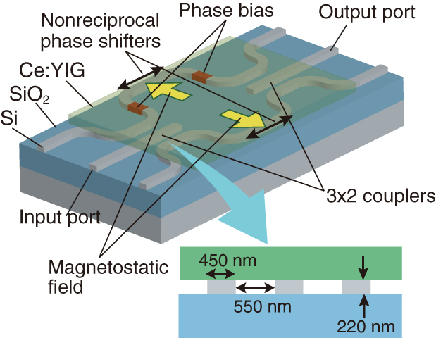
Schematic illustration of an SOI waveguide optical isolator based on MZI.
Because of the magneto-optical effect known as a non-reciprocal phase shift, a phase difference of Φ−–Φ+ occurs for the light wave propagating in the magneto-optical phase shifters from left to right. The phase difference can be set to −π/2 by adjusting the magneto-optical effect or length of magneto-optical phase shifter. This phase difference is canceled by the π/2 phase bias installed in the left arm. The phase bias can be realized by adjusting the optical path difference between the two waveguide arms. Hence, the light wave propagating in the waveguide arms becomes in phase and interferes constructively in the output 3 × 2 coupler. The light wave launched into the central input port of the left 3 × 2 coupler emerges at the central output port of the right 3 × 2 coupler. This corresponds to the forward direction.
For the backward direction, the phase difference produced by the magneto-optical effect changes its sign, i.e. Φ+ − Φ− = π/2. Because the remaining phase bias yields a π/2 phase difference in the left arm, a total phase difference of π is introduced between the two interferometer arms. Destructive interference occurs at the left coupler. The light wave does not come out at the initial input port, but instead is radiated out from the side waveguides of the 3 × 2 coupler.
The non-reciprocal phase shift Φ+–Φ− is calculated for a waveguide composed of a Ce:YIG cladding layer, silicon waveguide core and buried oxide (SiO2) under the cladding layer. The under cladding layer with a refractive index of 1.444 should be sufficiently thick so that the effects of the silicon substrate can be neglected. The upper cladding layer Ce:YIG is assumed to have a saturation Faraday rotation of θF = −4500° cm−1 and a refractive index of 2.20 at a calculated wavelength of 1550 nm. Figure 3 shows the calculated non-reciprocal phase shift as a function of the silicon waveguide core thickness. If we compare the non-reciprocal phase shift between a Ce:YIG/Si/SiO2 and Ce:YIG/GaInAsP/InP slab waveguide, the Ce:YIG/Si/SiO2 waveguide provides a much larger non-reciprocal phase shift than the Ce:YIG/GaInAsP/InP waveguide [36]. This can be understood by considering that the under cladding layer SiO2 has a much lower refractive index than InP (n = 3.17 at λ = 1550 nm). This results in a large penetration of the optical field into the upper cladding magneto-optical layer and consequently a larger magneto-optical effect. A non-reciprocal phase shift of 7.12 mm−1 can be obtained for the Ce:YIG/Si/SiO2 slab waveguide composed of a 200 nm-thick silicon waveguide core at a wavelength of 1550 nm.
Figure 3.
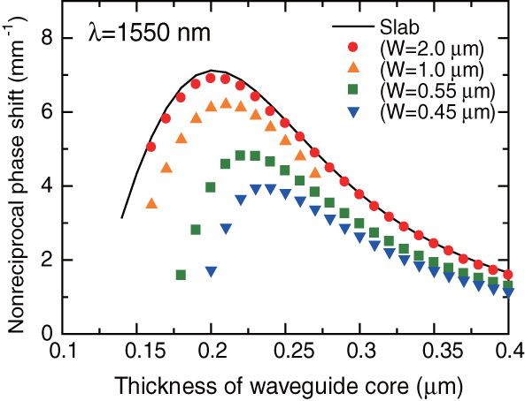
Calculated non-reciprocal phase shift at a wavelength of 1550 nm as a function of the silicon waveguide core thickness. The solid line corresponds to a slab waveguide. The plots represent the silicon rectangular waveguides of various widths W.
For a practical device, a three-dimensional waveguide such as a rib or rectangular core waveguide is used for the lateral optical field confinement. The non-reciprocal phase shift Φ+–Φ− is calculated in a silicon rectangular waveguide using (1), which was derived from perturbation theory [37, 38].
 |
where n and ε0 are the refractive index of Ce:YIG and vacuum permittivity, respectively. Hy denotes the distribution of the transverse magnetic field component of the TM mode in a waveguide. The integral is computed over the entire cross section of waveguide. γ denotes the off-diagonal component of the Ce:YIG permittivity tensor, which is related to the saturation Faraday rotation θF by
where λ is the wavelength of light.
The waveguide structure assumed in the calculation is shown in figure 4. It consists of a silicon rectangular waveguide core. The over and under cladding layers are Ce:YIG and SiO2, respectively. The side regions of the silicon waveguide core are assumed to be air.
Figure 4.
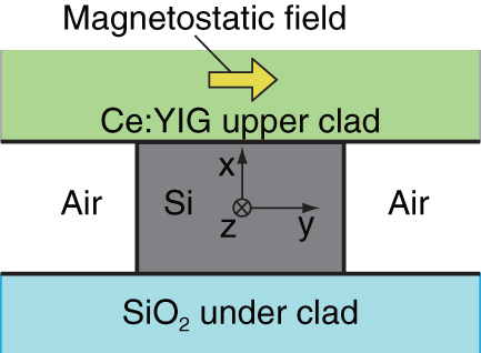
Waveguide structure assumed for calculating the magneto-optical phase shift in a silicon rectangular waveguide.
The calculated non-reciprocal phase shift that the fundamental TM guided mode experiences at a wavelength of 1550 nm is plotted as a function of the waveguide core thickness in figure 3 for various core widths W. The optical field distribution is calculated through a full vector finite element method. Compared to the slab waveguide, the non-reciprocal phase shift decreases in rectangular waveguides because the transverse field component in a Ce:YIG cladding layer is smaller. This tendency becomes prominent for narrower waveguides. The maximum non-reciprocal phase shift is obtained in a 200 nm-thick silicon slab waveguide. In the case of silicon rectangular waveguides with widths of 450 and 550 nm, the maximum non-reciprocal phase shift is obtained at the core thicknesses of 240 and 220 nm, respectively. Considering the specifications of commercially available SOI wafers, the device is designed in an SOI wafer with a 220 nm-thick top silicon layer. The length of the non-reciprocal phase shifter was calculated to be 430 and 327 μm for silicon waveguides having widths of 450 and 550 nm, respectively, for a 220 nm-thick silicon waveguide.
Non-reciprocal phase shifts are provided only for TM modes in vertically asymmetric waveguides as shown in figure 4. Non-reciprocal phase shifts are obtainable for TE modes when the magneto-optical material is placed in a horizontally asymmetric manner as is shown in figure 5. The MZI isolator that works for a TE mode can be realized using non-reciprocal phase shifters with the configuration shown in figure 5. Moreover, the polarization independent operation of a MZI isolator can be obtained by introducing both in-plane and out-of-plane asymmetric structures together with the proper magnetization of magneto-optical material [39]. In addition, the polarization independent isolator can be realized by adopting a proper design of an interferometer waveguide [40]. It is worth noting that the MZI based optical isolator can be extended to an optical circulator by replacing the 3 × 2 couplers with 3 dB directional couplers. This will be addressed in section 5.
Figure 5.
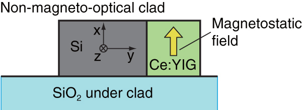
The cross sectional structure of a TE mode non-reciprocal phase shifter.
Fabrication and characterization
An SOI waveguide optical isolator based on an MZI was fabricated through the process shown in figure 6. An SOI wafer having a 220 nm-thick top silicon layer and a 3 μm-thick buried oxide layer is used in this device. Here, the thickness of the buried oxide layer was so chosen that the silicon substrate did not affect a fundamental TM mode propagating in the top silicon layer. The silicon waveguide pattern was drawn using an electron beam lithography system. Using a reactive ion etching (RIE) technique with CF4, the waveguide mask was transferred into a 300 nm-thick SiO2 layer deposited on the silicon guiding layer. The silicon rectangular waveguide of height 220 nm and width 450 nm was formed through SF6 RIE.
Figure 6.
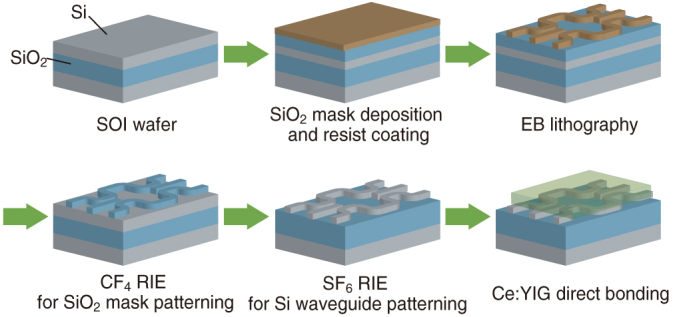
The fabrication process of an SOI waveguide optical isolator.
A single crystalline Ce:YIG layer was grown on a (111)-oriented SGGG substrate. The Ce:YIG layer was 500 nm-thick; this was sufficient for an evanescent field to be unaffected by the SGGG substrate. A 1.5 × 1.5 mm2 Ce:YIG die was directly bonded as an upper cladding layer using a surface activated direct bonding technique. Nitrogen plasma generated using an RF power of 500 W was applied for 10 s as a surface activation process. After bringing the two wafers into contact in a vacuum chamber, a pressure of 6 MPa was applied at 200 °C for 30 min [41].
In order to apply anti-parallel magnetic fields inside the two arms of the interferometer, a three pole magnet system composed of a pair of compact permanent magnets was used. A magnetic field of 16 kA m−1 was sufficient to saturate the magnetization of the Ce:YIG layer in the in-plane direction. The distance between the two arms of interferometer was fixed as 500 μm to accommodate the magnet. Because of the strong optical field confinement of the silicon waveguide in the lateral direction, the curved sections were designed with a curvature radius of 10 μm. By virtue of this, the device footprint was greatly reduced, as shown in figure 7, compared to the optical isolator fabricated with a silicon rib waveguide, which was 4 mm in length [15].
Figure 7.
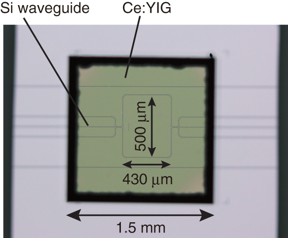
Microscope image of a fabricated MZI silicon waveguide optical isolator.
The fabricated isolator was characterized using the experimental setup shown in figure 8. A fundamental TM mode emitted from a broadband light source was introduced into the isolator through a polarization maintaining fiber (PMF). The transmitted light wave was probed using another PMF. Its spectrum was measured using an optical spectrum analyzer. A 2 × 2 optical switch was used to reverse the light propagation direction through the device/fiber test setup for measuring the forward and backward transmittance.
Figure 8.
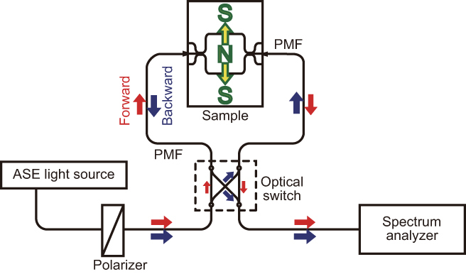
Experimental setup used for measurement of the fiber-to-fiber transmittance of an optical isolator.
Figure 9 shows the measured fiber-to-fiber transmittance under a fixed external magnetic field. The transmittance was observed to be remarkably different depending on the light propagation direction. The interference was also reversed when the magnetostatic field direction was reversed. This implies that the sign of the magneto-optical phase shift was reversed. The maximum isolation that was defined by the transmittance ratio of the forward to backward directions was measured to be 30 dB at a wavelength of 1548 nm. Compared to the transmittance of the reference waveguide without a Ce:YIG cladding layer, which included the propagation loss of a straight Si waveguide and 17 dB fiber-to-waveguide coupling losses at the input and output interfaces, the excess loss of the isolator was measured to be 13 dB. One of the causes of the insertion loss is the losses caused by the reflection and scattering at the interfaces between the air and Ce:YIG cladding regions. The loss is calculated to be 3.7 dB/interface at a wavelength of 1550 nm using an analysis based on the mode expansion algorithm. The losses can be reduced by depositing an upper cladding material having a refractive index of 2.20, which is close to that of Ce:YIG. The remaining loss of 5.6 dB can be attributed to the absorption of Ce:YIG and the bending losses of the curved waveguides included to form the MZI.
Figure 9.
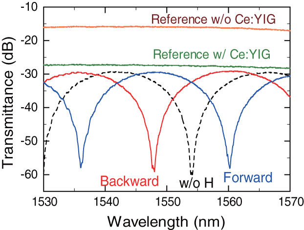
Measured fiber-to-fiber transmittance of the fabricated MZI silicon waveguide optical isolator as a function of the wavelength (blue and red lines) together with that of a non-magnetized device (broken line). The green and orange lines show the measured fiber-to-fiber transmittance of the reference waveguides with and without a Ce:YIG cladding layer, respectively.
The isolator exhibited a bandwidth of 1 nm, in which an optical isolation >20 dB was obtained. Because the phase bias was fixed at 100.5π, which is rather large compared to an ideal value of 0.5π, the free spectral range of the interferometer was greatly reduced. Hence, the isolation bandwidth was limited to 1 nm. When a phase bias of 0.5π is employed, the bandwidth of the optical isolations >20 dB is calculated to be 39 nm [42]. It is shown that the isolation bandwidth can be increased further by canceling the wavelength dependence of the magneto-optical phase shift with that of the phase bias [43].
Ghosh et al [44] demonstrated a silicon MZI optical isolator with an isolation of 25 dB. The advantage of this device is that it operates in a unidirectional magnetostatic field. They bonded a Ce:YIG die on a silicon MZI waveguide through an adhesive benzocyclobutene (BCB) bonding technique. A Ce:YIG layer was grown on an SGGG substrate through a sputter epitaxial growth technique. It should be noted that since the evanescent field penetrating the Ce:YIG layer is responsible for the magneto-optical phase shift, the thickness of intermediate layer between the silicon and garnet must be stringently controlled in order to obtain the desired magneto-optical phase shift [45].
Ring resonator based optical isolator
When the magneto-optical phase shifter is included in a ring resonator, the light wave propagating in the resonator experiences the direction-dependent phase shift. Therefore, the resonator exhibits different resonant wavelengths between the clock-wise and counter-clock-wise propagating light waves. This can be achieved by placing a magneto-optical material as an upper cladding layer on the ring resonator and by applying a magnetostatic field along the radial direction of the ring. Because of the different resonant wavelengths, the transmittance of the bus-line coupled to the ring resonator becomes direction-dependent. Thus, the optical isolation is obtained around the resonant wavelength of the backward propagating light wave.
Tien et al [46] fabricated a ring resonator based optical isolator by directly bonding a Ce:YIG die on a silicon ring resonator. They demonstrated an isolation of 9 dB by reversing the direction of the applied magnetostatic field.
Bi et al [47] deposited a magneto-optical garnet bilayer on a silicon racetrack resonator partially through a window in the SiO2 cladding layer. They deposited a 20 nm-thick YIG seed layer on silicon, and then deposited (Ce1Y2)Fe5O12 on the YIG seed layer through PLD. An isolation ratio of 19.5 ± 2.9 dB was reported with an insertion loss of approximately 19 dB. Since the isolation of these isolators is provided near the resonant wavelength of a backward propagation light wave, the isolation bandwidth is limited by the response of the ring resonator.
Magneto-optical circulator
A silicon waveguide optical circulator can be built by replacing the 3 × 2 couplers of the MZI optical isolator with 3 dB directional couplers as shown in figure 10 [48]. For the rightward propagation, the non-reciprocal phase shifter gives a phase difference of −π/2, while the phase bias gives a phase difference of π/2 between the left and right arms. The light wave introduced into port 1 is divided between the two interferometer arms using a 3 dB directional coupler; the light wave then passes through the non-reciprocal phase shifters and phase bias and is combined in an output 3 dB directional coupler. The light wave propagating through the two arms becomes in-phase and forms the output from the cross port, which is port 2.
Figure 10.
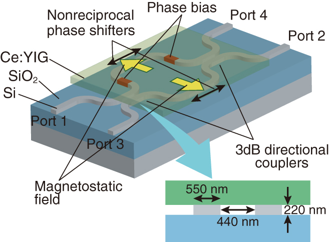
Schematic illustration of an SOI waveguide optical circulator.
On the other hand, for leftward propagation, the light wave introduced into port 2 experiences a non-reciprocal phase difference of π/2. The total phase difference between the two arms amounts to π because the remaining phase bias yields a π/2 phase difference. Therefore, the light wave emerges at the bar port, which is port 3, instead of port 1. Likewise, the light wave input at port 3 is directed to port 4, and the input at port 4 is directed to port 1. Thus, a complete 4 port circulator operation is achieved.
The 3 dB directional coupler used to construct a MZI was designed with 550 nm-wide and 220 nm-high silicon waveguides placed in parallel. The spacing between the two waveguides was chosen to yield a maximum tolerance with respect to the deviation in waveguide width for a given distance between the centers of the two waveguides. The coupling length was calculated to be 24.5 μm for a waveguide spacing of 440 nm. The length of the non-reciprocal phase shifter was calculated to be 327 μm for the 550 nm-wide and 220 nm-thick silicon rectangular waveguide.
Following the same fabrication procedure as the MZI silicon waveguide optical isolator, a waveguide optical circulator was fabricated in a 220 nm-thick silicon top layer on an SOI wafer with a 3.0 μm-thick buried oxide layer. We measured the fiber-to-fiber transmittance of a fabricated device for different input/output port combinations to demonstrate a circulator function. A magnetostatic field was applied to the Ce:YIG bonded to the interferometer arms along outward, anti-parallel directions using a pair of compact three pole permanent magnets. By exchanging the propagation direction using a 2 × 2 optical switch, the transmittance was measured for the counter propagating directions while maintaining an applied magnetostatic field and a fiber-device-fiber connection.
Figure 11 shows the fiber-to-fiber transmittance spectra measured between the cross ports (ports 1 and 2). The measured transmittance of the straight reference waveguide without a Ce:YIG cladding layer is also shown in figure 11. It is observed that the device exhibits a non-reciprocal performance by comparing the counter propagating transmittances indicated by the red (from port 1 to 2) and blue (from port 2 to 1) lines in figure 11.
Figure 11.
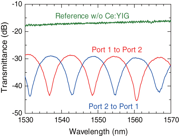
Measured fiber-to-fiber transmittance of a fabricated SOI waveguide optical circulator between ports 1 and 2. © 2013 IEEE. Reprinted, with permission, from [49].
The transmittance measured at 1531 nm is summarized in table 1 for the four input/output port combinations. An input from port 1 is mainly conducted to port 2, whereas an input from port 2 is conducted to port 3 instead of port 1. Likewise, inputs from ports 3 and 4 are conducted to ports 4 and 1, respectively, at this wavelength. On the other hand, ports 4, 1, 2 and 3 are the isolating ports for the input from ports 1, 2, 3 and 4, respectively. Forward-to-backward isolation is defined as the transmittance ratio of the counter propagating directions for a given port pair. Isolations of 15.3 and 13.1 dB are obtained for the cross port pairs of ports 1 and 2 and ports 3 and 4, respectively, whereas for the bar port pairs, isolations of 9.3 and 6.7 dB are obtained for ports 2 and 3 and ports 4 and 1, respectively [49]. The reason for the isolation measured in the bar ports being less than that in the cross ports is mainly the deviation of a dividing characteristic from exactly 3 dB in the directional couplers. The isolation of the bar port can be improved by adjusting the coupling length of the directional couplers for controlling the dividing ratio. The isolation of the cross port can be improved by reducing the fabrication errors so that the couplers have identical performance characteristics.
Table 1.
Transmittance for the input/output port combinations measured at a wavelength of 1531 nm [49].
| Transmittance measured at output (dB) | ||||
|---|---|---|---|---|
| Input | Port 1 | Port 2 | Port 3 | Port 4 |
| Port 1 | – | −28.4 | – | −34.5 |
| Port 2 | −43.7 | – | −28.0 | – |
| Port 3 | – | −37.3 | – | −29.0 |
| Port 4 | −27.8 | – | −42.1 | – |
The measured transmittance of the reference waveguide includes a coupling loss of 8 dB/facet between the fiber and silicon wire waveguide. The propagation loss of an air clad silicon waveguide is estimated to be 0.27 dB mm−1 at a wavelength of 1550 nm. Compared to the insertion loss of the reference waveguide, the excess loss of the fabricated circulator is estimated to be 11.5 dB at a wavelength of 1550 nm. One of the causes of the excess circulator loss is the losses due to the reflection and scattering at the interfaces between the air and Ce:YIG cladding regions. The loss is calculated to be 3.2 dB per interface at a wavelength of 1550 nm through an analysis based on the mode expansion algorithm. The remaining loss of 5.1 dB can be attributed to the absorption in the Ce:YIG layer and the excess bending losses of curved waveguides included to form the MZI.
Conclusions
Optical non-reciprocal devices developed on silicon waveguide platforms were reviewed. The magneto-optical effect plays an important role to obtain an optical non-reciprocal function. Two different approaches, deposition and bonding, were investigated for integrating a magneto-optical garnet on a silicon waveguide. Compared to state-of-the-art deposition techniques, the bonding technique is advantageous because a single-crystalline magneto-optical garnet containing a large Faraday rotation can be used. This reduces the required magneto-optical interaction length. We developed the surface activated direct bonding technique to integrate a magneto-optical garnet on a silicon waveguide. As a surface activation process, it was shown that the oxygen or nitrogen plasma irradiation was effective for bonding a garnet on a silicon waveguide. This technique was applied to fabricate an MZI silicon waveguide optical isolator and circulator that use the magneto-optical phase shift. The low refractive index of a buried oxide layer enhances the magneto-optical phase shift in an SOI waveguide. The performance of the MZI silicon waveguide optical isolator was demonstrated with an isolation of 30 dB at a wavelength of 1548 nm. In addition, a maximum isolation of 15.3 dB was obtained in an optical circulator fabricated with a silicon MZI waveguide.
References
- Petermann K. 1995. External optical feedback phenomena in semiconductor lasers IEEE J. Sel. Top. Quantum Electron. 1 480–9 [Google Scholar]
- Shirasaki M and Asama K. 1982. Compact optical isolator for fibers using birefringent wedges Appl. Opt. 21 4296–99 [DOI] [PubMed] [Google Scholar]
- Chang K W and Sorin W V. 1989. Polarization independent isolator using spatial Walkoff polarizers IEEE Photon. Technol. Lett. 1 68–70 [Google Scholar]
- Fujii Y. 1991. High-isolation polarization-independent optical circulator J. Lightw. Technol. 9 1238–43 [DOI] [PubMed] [Google Scholar]
- Wang S, Shah M and Crow J D. 1972. Studies of the use of gyrotropic and anisotropic materials for mode conversion in thin-film optical-waveguide applications J. Appl. Phys. 43 1861–75 [Google Scholar]
- Warner J. 1973. Faraday optical isolator/gyrator design in planar dielectric waveguide form IEEE Trans. Microw. Theory Tech. MTT–21 769–75 [Google Scholar]
- Hepner G, Desormiere B and Castera J P. 1975. Magnetooptic effect in garnet thin film waveguides Appl. Opt. 14 1479–81 [DOI] [PubMed] [Google Scholar]
- Ando K, Okoshi T and Koshizuka N. 1988. Waveguide magneto-optic isolator fabricated by laser annealing Appl. Phys. Lett. 53 4–6 [Google Scholar]
- Mizumoto T, Kawaoka Y and Naito Y. 1986. Waveguide-type optical isolator using the Faraday and Cotton–Mouton effects Trans. IEICE E69 968–72 [Google Scholar]
- Wolfe R, Fratello V J and McGlashan-Powell M. 1988. Thin-film garnet materials with zero linear birefringence for magneto-optic waveguide devices J. Appl. Phys. 63 3099–103 [Google Scholar]
- Levy M. 2002. The on-chip integration of magnetooptic waveguide isolators IEEE J. Sel. Top. Quantum Electron. 8 1300–6 [Google Scholar]
- Hansen P and Krume J P. 1984. Magnetic and magneto-optical properties of garnet films Thin Solid Films 114 69–107 [Google Scholar]
- Takei R, Yoshida K. and Mizumoto T. Effect of wafer pre-cleaning and plasma irradiation to wafer surfaces for plasma-assisted surface activated bonding. Japan. J. Appl. Phys. 2010;49:086204. [Google Scholar]
- Mizumoto T, Shoji Y and Takei R. Direct wafer bonding and its application to waveguide optical isolators Materials 5 985–1004 [DOI] [PMC free article] [PubMed] [Google Scholar]
- Shoji Y, Mizumoto T, Yokoi H, Hsieh I W, Osgood R M., Jr Magneto-optical isolator with silicon waveguides fabricated by direct bonding. Appl. Phys. Lett. 2008;92:071117. [Google Scholar]
- Sobu Y, Shoji Y, Sakurai K and Mizumoto T. 2013. GaInAsP/InP MZI waveguide optical isolator integrated with spot size converter Opt. Express 21 15373–81 [DOI] [PubMed] [Google Scholar]
- Yu Z and Fan S. 2009. Complete optical isolation created by indirect interband photonic transitions Nature Photon. 3 91–4 [Google Scholar]
- Fan L, Wang J, Varghese L T, Shen H, Niu B, Xuan Y, Weiner A M and Qi M. 2012. An all-silicon passive optical diode Science 335 447–50 [DOI] [PMC free article] [PubMed] [Google Scholar]
- Stadler B J H and Gopinath A. 2000. Magneto-optical garnet films made by reactive sputtering IEEE Trans. Magn. 36 3957–61 [Google Scholar]
- Sung S-Y, Qi X. and Stadler B J H. Integrating yttrium iron garnet onto nongarnet substrates with faster deposition rates and high reliability. Appl. Phys. Lett. 2005;87:121111. [Google Scholar]
- Körner T, Heinrich A, Weckrle A, Roocks P. and Stritzker B. Integration of magneto-optical active bismuth iron garnet on nongarnet substrates. J. Appl. Phys. 2008;103:07B337. [Google Scholar]
- Bi L, Hu J, Dionne G F, Kimerling L. and Ross C A. Monolithic integration of chalcogenide glass/iron garnet waveguides and resonators for on-chip nonreciprocal photonic devices. Proc. SPIE. 2011;7941:794105. [Google Scholar]
- Shintaku T and Uno T. 1994. Optical waveguide isolator based on nonreciprocal radiation J. Appl. Phys. 76 8155–9 [Google Scholar]
- Takagi H, Maeda R and Suga T. 2001. Room-temperature wafer bonding of Si to LiNbO3, LiTaO3 and Gd3Ga5O12 by Ar-beam surface activation J. Micromech. Microeng. 11 348–52 [Google Scholar]
- Suga T, Kim T H. and Howlader M M R. Combined process for wafer direct bonding by means of the surface activation method. Proc. 54th Electronic Components and Technology Conf.; Las Vegas. USA, 1–4 June 2004); 2004. (New Jersey: The Institute of Electrical and Electronics Engineers) pp 484–90. [Google Scholar]
- Pasquariello D and Hjort K. 2002. Plasma-assisted InP-to-Si low temperature wafer bonding IEEE J. Sel. Top. Quantum Electron. 8 118–31 [Google Scholar]
- Auracher F and Witte H H. 1975 A. new design for an integrated optical isolator Opt. Commun. 13 435–8 [Google Scholar]
- Mizumoto T and Naito Y. 1982. Nonreciprocal propagation characteristics of YIG thin film IEEE Trans. Microw. Theory Tech. MTT–30 922–5 [Google Scholar]
- Mizumoto T, Oochi K, Harada T and Naito Y. 1986. Measurement of optical nonreciprocal phase shift in a Bi-substituted Gd3Fe5O12 film and application to waveguide-type optical circulator J. Lightw. Technol. LT–4 347–52 [Google Scholar]
- Okamura Y, Inuzuka H, Kikuchi T and Yamamoto S. 1986. Nonreciprocal propagation in magnetooptic YIG rib waveguide J. Lightw. Technol. LT–4 711–4 [Google Scholar]
- Yokoi H, Mizumoto T, Takano T and Shinjo N. 1999. Demonstration of an optical isolator by use of a nonreciprocal phase shift Appl. Opt. 38 7409–13 [DOI] [PubMed] [Google Scholar]
- Fujita J, Levy M Osgood R M Jr., Wilken L and Dötsch H. 2000. Waveguide optical isolator based on Mach–Zehnder interferometer Appl. Phys. Lett. 76 2158–60 [Google Scholar]
- Yokoi H, Mizumoto T and Shoji Y. 2003. Optical nonreciprocal devices with a silicon guiding layer fabricated by wafer bonding Appl. Opt. 42 6605–12 [DOI] [PubMed] [Google Scholar]
- Espinola R L, Izuhara T, Tsai M-C Osgood R M Jr and Dötsch H. 2004. Magneto-optical nonreciprocal phase shift in garnet/silicon-on-insulator waveguides Opt. Lett. 29 941–3 [DOI] [PubMed] [Google Scholar]
- Yokoi H and Mizumoto T. 1997. Proposed configuration of integrated optical isolator employing wafer-direct bonding technique Electron. Lett. 33 1787–8 [Google Scholar]
- Mizumoto T, Takei R and Shoji Y. 2012. Waveguide optical isolators for integrated optics IEEE J. Quantum Electron. 48 252–60 [Google Scholar]
- Yamamoto S and Makimoto T. 1974. Circuit theory for a class of anisotropic and gyrotropic thin-film optical waveguides and design of nonreciprocal devices for integrated optics J. Appl. Phys. 45 882–8 [Google Scholar]
- Zhuromskyy O, Lohmeyer M, Bahlmann N, Dötsch H, Hertel P and Popkov P F. 1999. Analysis of polarization independent Mach–Zehnder-type integrated optical isolator J. Lightw. Technol. 17 1200–5 [Google Scholar]
- Fujita J, Levy M Osgood R M Jr, Wilkens L and Dötsch H. 2000. Polarization-independent waveguide optical isolator based on nonreciprocal phase shift IEEE Photon. Technol. Lett. 12 1510–2 [Google Scholar]
- Shoji Y, Hsieh I-W Osgood R M Jr and Mizumoto T. 2007. Polarization-independent magneto-optical waveguide isolator using TM-mode nonreciprocal phase shift J. Lightw. Technol. 25 3108–13 [Google Scholar]
- Shirato Y, Shoji Y and Mizumoto T. 2013. High isolation in silicon waveguide optical isolator employing nonreciprocal phase shift Technical Digest Optical Fiber Communication Conf. and Exposition and National Fiber Optic Engineers Conf. Anaheim, USA 17–21 March 2013 Washington, DC: Optical Society of America; OTu2C.5 [Google Scholar]
- Shirato Y, Shoji Y. and Mizumoto T. Over 20-dB isolation with 8-nm bandwidth in silicon MZI optical isolator. Technical Digest the 10th Int. Conf. on Group IV Photonics; Seoul, Korea. 28–30 August 2013; 2013. (New Jersey: The Institute of Electrical and Electronics Engineers) FA4. [Google Scholar]
- Shoji Y and Mizumoto T. 2007. Ultra-wideband design of waveguide magneto-optical isolator operating in 1.31 and 1.55 μm band Opt. Express 15 639–45 [DOI] [PubMed] [Google Scholar]
- Ghosh S, Keyvavinia S, Roy W V, Mizumoto T, Roelkens G and Baets R. 2012 A. Ce:YIG/silicon-on-insulator waveguide optical isolator realized by adhesive bonding Opt. Express 20 1839–48 [DOI] [PubMed] [Google Scholar]
- Shoji Y, Itoh M, Shirato Y and Mizumoto T. 2012. MZI optical isolator with Si-wire waveguides by surface-activated direct bonding Opt. Express 20 18440–8 [DOI] [PubMed] [Google Scholar]
- Tien M-C, Mizumoto T, Pintus P, Kromer H and Bowers J. 2011. Silicon ring isolators with bonded nonreciprocal magneto-optic garnets Opt. Express 19 11740–5 [DOI] [PubMed] [Google Scholar]
- Bi L, Hu J, Jiang P, Kim D H, Dionne G F, Kimerling L C and Ross C A. 2011. On-chip optical isolation in monolithically integrated non-reciprocal optical resonators Nature Photon. 5 758–62 [Google Scholar]
- Takei R. and Mizumoto T. Design and simulation of silicon waveguide optical circulator employing nonreciprocal phase shift. Japan. J. Appl. Phys. 2010;49:052203. [Google Scholar]
- Mitsuya K, Shoji Y and Mizumoto T. 2013. Demonstration of a silicon waveguide optical circulator IEEE Photon. Technol. Lett. 25 721–3 [Google Scholar]


