Abstract
We report the surface functionalization of graphene films grown by chemical vapor deposition and fabrication of a hybrid material combining multi-walled carbon nanotubes and graphene (CNT–G). Amine-terminated self-assembled monolayers were prepared on graphene by the UV-modification of oxidized groups introduced onto the film surface. Amine-termination led to effective interaction with functionalized CNTs to assemble a CNT–G hybrid through covalent bonding. Characterization clearly showed no defects of the graphene film after the immobilization reaction with CNT. In addition, the hybrid graphene material revealed a distinctive CNT–G structure and p–n type electrical properties. The introduction of functional groups on the graphene film surface and fabrication of CNT–G hybrids with the present technique could provide an efficient, novel route to device fabrication.
Keywords: Chemical vapor deposition-grown graphene film, Self-assembled monolayer, Multi-walled carbon nanotubes, Hybrid characterization
1. Introduction
Graphene has emerged as a new class of materials [1] that has attracted tremendous attention because of its remarkable physical, electrical and optical properties [2–6]. Such properties have encouraged studies of graphene for potential applications in solar cells, field-emission devices, field-effect transistors, supercapacitors and batteries [7–9]. Unfortunately, the configuration and manipulation of graphene is difficult owing to its hydrophobic nature [10], which remains a significant challenge for its utilization at the macroscopic level [11]. In this context, functionalization of graphene film is important for controllable processing. As yet, most methods for ascribing molecules onto graphene have concentrated on non-covalent π-bond stacking [12] or have utilized graphene oxide (graphene sheets) [13–15].
In recent times, considerable effort has focused on the self-assembly and chemical modification of graphene films, in which most covalent functionalization experiments have typically relied on reactive diazonium salts [16], azides [17] or halogenation reactions [18, 19]. However, most of the above techniques suffer from a lack of active terminal group/property control, leading to inadequate handles for further chemical bonding to other materials (likewise; CNT). Moreover, graphene hybrid materials with interconnected networks may have superior durability/applicability features for use in flexible devices. Therefore, CNT immobilization onto functionalized CVD graphene film would be highly desirable for the establishment of uninterrupted CNT–graphene networks. To realize the merits of combined two-dimensional (2D) graphene and one-dimensional CNT nanocarbon materials, there have been many recent attempts to obtain graphene sheet–CNT hybrid materials or composites. For this instance, Yu and Dai [20] prepared a graphene sheet/CNT hybrid film with interconnected networks, for use in supercapacitors. In addition, attempts have been made to fabricate graphene sheet/CNT hybrid film by spin-coating homogeneously mixed solutions of the two carbon-based nanomaterials [21], as well as using a solid-phase layer stacking approach with ethanol wetting [22].
Here, we report a simple approach to activate CVD-grown graphene film through self-assembled monolayer (SAM) fabrication followed by UV treatment, which creates an efficiently oxidized film surface. To the best of our knowledge, the utility of UV-treatment for fabrication of SAM on CVD-grown graphene film and the preparation of CNT–G hybrid material through chemical bonding have not yet been reported. This method could be useful as a new route to the fabrication of graphene hybrid materials for a variety of potential applications.
Experimental details
Materials
HNO3, CHCl3, UV-lamp (Viber Lourmat, UV System, France), 3-aminopropyltriethoxysilane (APTES), 0.5 M FeCl3 solution, toluene, ethanol, CNTs (ILJIN, Nanotech), cellulose membrane filter paper (1 μm pore size) and ultrasonicator (100 W, 60 Hz), were commercial products that were used as received. Deionized water was used in all experiments.
Preparation of CVD graphene film
Graphene was grown on copper (Cu) by atmospheric pressure CVD using methane as a carbon source. The reaction was carried out at 1050 °C for 20 min with a mixture flow of H2/methane of 100/10 sccm. After the reaction, the Cu foil was cooled to room temperature under an H2 environment. To obtain free-standing graphene film, the Cu foil was etched with 0.5 M FeCl3 solution. The detached graphene film was rinsed with deionized water and freely floating film on the water surface was transferred onto a SiO2/Si substrate (G/Si) [23].
Surface functionalization of graphene film
APTES solution was deposited onto G/Si in the vapor phase. Before the actual fabrication process, a pretreatment step was used to terminate the G/Si surface with OH groups. The pretreatment step involved UV-irradiation for 30 min (UV-G/Si). Then, a glass beaker containing the UV-treated G/Si and 1% APTES/toluene solution was placed in an air-tight steel box. The box was loaded into the processing chamber. Upon heating at 115 °C for 2 h, the silane precursor evaporated into the inner processing chamber space to create a saturated atmosphere consisting of coating molecules that reacted with the UV-G/Si to form SAM deposition. Next, the functionalized graphene was thoroughly sonicated for 10 s, rinsed with toluene and ethanol, and then dried under a stream of N2 gas (SAM-G/Si).
Surface functionalization of carbon nanotubes
Acid functionalization of multi-walled carbon nanotubes (CNTs) was carried out by oxidation of CNTs with 60% HNO3. CNTs (30 mg) and HNO3 (60 ml) were mixed in a flask equipped with a condenser. The mixture was heated to 80 °C overnight. The resulting CNTs were vacuum filtered, and rinsed with deionized water until the pH was neutral. This material was heated to 60 °C in a vacuum oven for 1 h.
Preparation of CNT–G hybrid material
The acid-treated CNTs were ultrasonically dispersed in chloroform solution. The SAM-G/Si substrate was immersed in the solution, and the reaction mixture was kept overnight at 45 °C. The substrate was then removed from the mixture, sonicated for 10 s and rinsed with ethanol to remove unabsorbed CNTs. The immobilized CNT on SAM-G/Si is referred to as CNT–G/Si (graphene hybrid material) and is shown in figure 1.
Figure 1.

Schematic of the preparation process of surface-functionalized graphene film and fabrication of CNT–G hybrid material.
Characterization
Surface modified G/Si substrates were characterized by x-ray photoelectron spectroscopy (XPS). XPS spectra were obtained using a theta probe (VGMICROTEC, ESCA 2000) with a monochromatic AlKα source at a pressure of 2 × 10⁻⁹ mbar. Raman spectra were obtained using a Renishaw 1000 micro-Raman spectrometer at an excitation wavelength of 514 nm where at least three different sites on each sample were evaluated. Graphene topography before and after SAM fabrication was evaluated by an atomic force microscope (AFM, SPA 400). Fourier-transform infrared spectroscopy (FTIR, Bruker, IFS 66/S) was used to detect the characteristic absorbance of functional groups grafted on the graphene hybrid material. Surface functionalization of CNTs was evaluated by FTIR and XPS. The surface morphology of samples was characterized using a field emission scanning electron microscope (FESEM, JEOL, JSM-7500F) at an accelerating voltage of 15 kV. Formation of the CNT–G/Si hybrid structure was studied using a high-resolution transmission electron microscope (HRTEM, JEOL, JEM2100F). Electrical properties were examined using a Keithley 4200-SCS semiconductor analyzer.
Results and discussion
Characterization of SAM-G/Si
XPS was employed to check the surface functionalization of graphene film. Figure 2 shows survey scan spectra collected from G/Si, UV-G/Si and SAM-G/Si (figures 2(a), (c) and (e)). The most prominent peaks were C1s and O1s for all sample scans. However, the appearance of an N1s peak centered at 401 eV was observed only for SAM-G/Si (figure 2(e)). In addition, C1s and O1s peaks were fitted by the deconvolution procedure as shown in figure S1 (available at stacks.iop.org/STAM/15/015007/mmedia). Nevertheless, as associated to their intensities the variations of core peak position were not so large for each of them and it would be difficult to analyze components quantitatively. In the meantime, the C/O ratio for G/Si was 1.6, whereas after UV-treatment, it decreased to 1.4, suggesting an increase of oxygen-containing moieties on UV-G/Si. But, after SAM fabrication on a UV-treated sample, the C/O ratio increased up to 2.2, indicating the increase of carbon-containing molecules can be attributed to the carbons of SAM. Therefore, the XPS study confirmed the transformation of functionalization after surface treatment and signifies the presence of the amine-terminated SAM on the graphene surface [24], which demonstrated that UV treatment provided an efficient surface on graphene for SAM fabrication.
Figure 2.
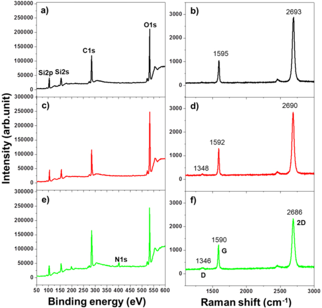
XPS survey spectra profile and Raman spectra for G/Si (a) and (b), UV-G/Si (c) and (d) and SAM-G/Si (e) and (f).
Next, Raman analyses of SAM-G/Si were performed and compared with G/Si, and UV-G/Si as shown in figure 2. The G peak for G/Si was observed at ∼1595 cm−1 (figure 2(b)), which arose from the high-frequency E2g phonon mode [25]. The 2D peak, observed at ∼2693 cm−1 (from excitation at 514 nm), was a second-order vibration caused by the scattering of two phonons [26]. Changes of the G peak after UV irradiation and SAM fabrication are shown in figures 2(d) and (f), in which the G peak shifted from 1595 to ∼1592 cm−1. After SAM deposition, the G peak moved ∼2 cm−1 toward the lower energy region. The 2D peak also shifted from ∼2693 cm−1 to lower energy by ∼3 cm−1 after UV irradiation and further shifted ∼4 cm−1 lower after amine-SAM fabrication which might be adapted n-type behavior due to n-doping induced by SAM (figure 2(f)). Das et al [27] demonstrated that n-doping of graphene caused the 2D Raman band to shift downward. Typically, n-type doped graphene or adsorption of molecules with electron-donating groups, G band downshifts [6]. In this study, shifts of the G and 2D peaks in the same direction after surface treatment were observed. However, the intensity of the 2D band decreased after functionalization, due to the interaction with functionalized molecules, which clearly indicate an increase of functional sites on the graphene surface. Thus, the molecular conformation has changed from trans to cis due to surface functionalization, which causes interactions between graphene and the functionalized groups [28].
AFM measurements were performed in the tapping mode to characterize surface topography changes of graphene film before and after SAM fabrication as shown in figure 3. A useful description of surface topography was given by the surface roughness [29]. The AFM image of G/Si displayed a lower root mean square (RMS) value (1.5 nm) and non-uniform islands that come from a low level of functional group [30] as shown in figure 3(a). From the micrographs, it was noticeable that the surface topography of SAM-fabricated graphene film was quite uniform and homogeneous; however, a higher rms value (1.9 nm) was observed as shown in figure 3(b), indicating the existence of substantial functional groups. It was expected that the SAM-G/Si film would be thicker than G/Si as a result of surface functionalization. Importantly, this result indicated that control of the-functionalization density by changing the extent of UV-treatment might be useful. These AFM results were in agreement with the XPS and Raman analyses.
Figure 3.
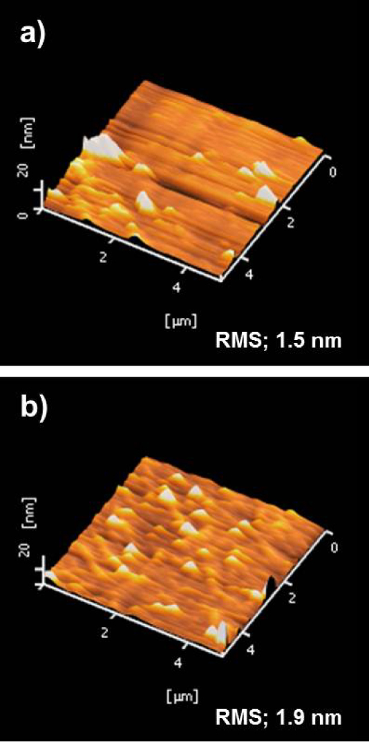
AFM topography for G/Si (a) and SAM-G/Si (b).
Characterization of acid-treated CNTs
The surface-functionalized CVD graphene film was used to bind surface-modified CNTs. The acid functionalized CNTs were checked by Raman spectroscopy, XPS and FTIR, and spectra from pristine CNTs were used as a reference. For both CNTs samples, D (1350 cm−1), G (1594 cm−1) and 2D (2695 cm−1) bands were seen as shown in figures S2a and S2c (supporting information S2 available at stacks.iop.org/STAM/15/015007/mmedia). However, the spectrum of acid-treated CNTs showed a strong D peak attributable to significant structural defect sites formed from oxidation [31, 32]. Meanwhile, raw XPS data for both samples were analyzed to determine peak locations as shown in figures S2b and S2d. Aside from the main C = C peak at 284.6 eV, extra peaks at higher binding energies for pristine and functionalized CNTs indicated the presence of carbon atoms bound to other functional groups. The binding energy peak at 286.1 eV for pristine CNTs was attributed to atmospheric oxidation or residual oxides [32]. Similarly, for the functionalized CNT sample, –C–O and –OH–C = O (carboxylic acid) contribute [33–35]. These results are consistent with the Raman measurements as shown in figure S1c. To confirm oxygen containing functional groups, FTIR measurement was employed. FTIR spectra of pristine and acid-treated CNTs are shown in figure S3 (available at stacks.iop.org/STAM/15/015007/mmedia). Pristine CNTs displayed an absorption band at 3435 cm−1, which resulted from a trace amount of water [36]. The IR spectrum of acid-treated CNTs exhibited additional bands at 1730, 1521 and 1386 cm−1, which were assigned to C = O, COO− and C–O stretching vibration modes, indicating the coexistence of carboxylic acid and carboxylate groups [37]. Thus, FTIR analysis confirmed the surface functionalization of CNTs.
Characterization of immobilized CNT on functionalized graphene film
CNT immobilized on the SAM graphene surface (CNT–G/Si) was characterized by Raman spectroscopy as shown in figure 4. When compared with acid-treated CNTs and SAM-G/Si spectra (figures 4(a) and (b)), differences in the G (1591 cm−1) and 2D (2687 cm−1) peak widths, positions and their intensity ratio for CNT–G/Si (figure 4(c)) was indicative of CNT hybridization with graphene. It was notable that the D band was prominent after CNT adsorption, which was useful for evaluating the combination state of CNT on the graphene surface. Figure 4(a), shows the peak positions of acid-treated CNTs, with G, D and 2D bands at 1594, 1359 and 2695 cm−1, respectively, which were all up-shifted compared to the SAM-G/Si bands (figure 2(d)). Moreover, the G and 2D peak positions were lower for CNT–G/Si than for the acid-treated CNTs but higher than for SAM-G/Si. However, these values are lower than for graphene without functionalization with APTES (figure 2(b)) and are indicative of a reduction in the p-type state. Furthermore, core peaks for the D, G and 2D bands were fitted to locate the position of CNT and graphene separately into them as shown in figure 4(c) (inset). But, only the G band has shown a noticeable two peak position as compared to the D band, where lower (1581 cm−1) and higher (1602 cm−1) shifted peaks appeared that should come from graphene and CNT respectively. Moreover, CNT can be attributed to induce p-type behavior after hybridization. For, p-type doped graphene, or adsorption of molecules with electron-withdrawing groups, it upshifts and softens while it is in contrast for n-type [6]. Likewise, the upshift of the G band position and the downshift of the 2D band position suggests n-doping of graphene, whereas upshifts of the G band and the 2D band positions implies p-doping due to the phonon stiffening effect from charge extraction [27]. Conversely, both G and 2D bands were a bit upshifted after CNT immobilization, with an apparent reduction of the n-type state. However, both n-type and p-type characteristic features might remain in the hybrid material because of chemical bonding between CNT and graphene.
Figure 4.
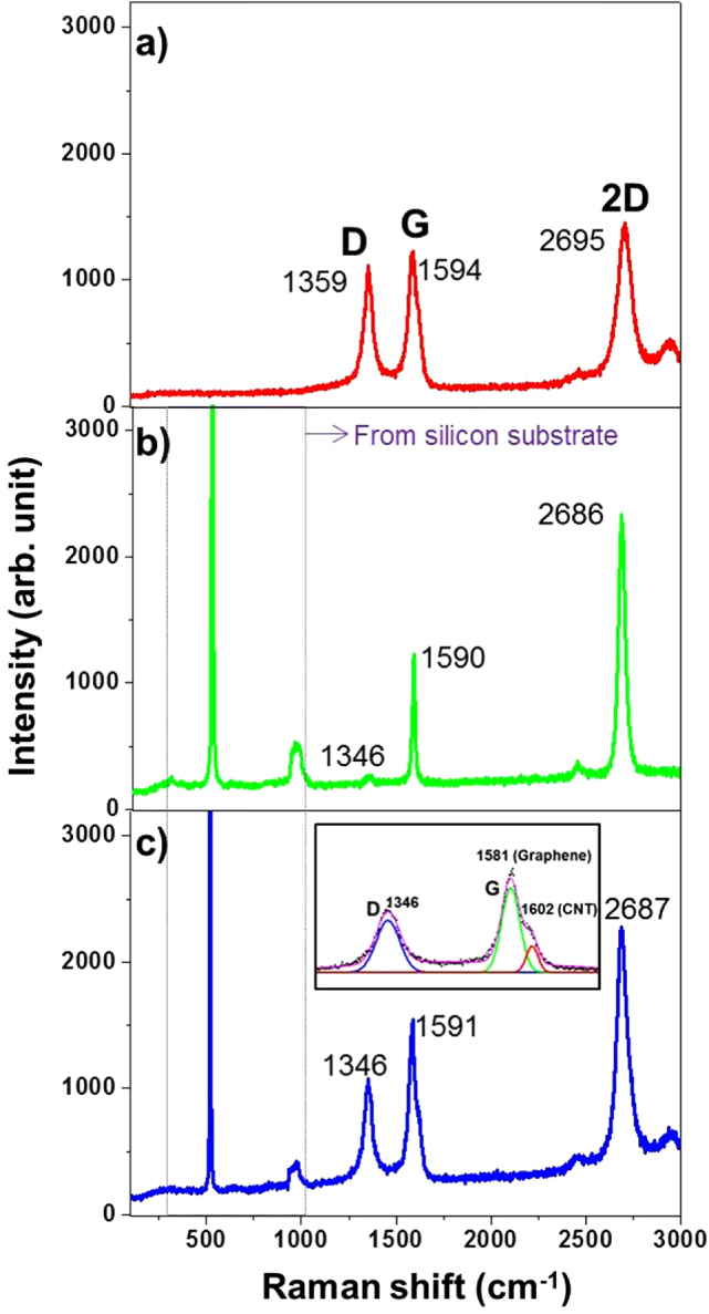
Raman spectra for acid-treated CNTs (a), SAM-G/Si (b) and CNT–G/Si (c); (inset; approximation of G peak for graphene and CNT).
Moreover, the G/D ratio of acid-treated CNTs, SAM-G/Si and CNT–G/Si were found of the order of 1.0, 4.4 and 1.5 respectively, which indicates that the value of the G/D ratio of the SAM-containing sample was reduced after CNT adsorption. This adsorption modulation by immobilization technique was further studied by XPS, FTIR and electrical transport measurements.
Possible binding between CNT and graphene was further performed in an XPS study of the N1s peak (figure 5). For free amines, the N1s peak position was observed at a binding energy of 401 eV (figure 5(a)). The XPS pattern of CNT–G/Si was used to investigate the chemical bonding state. The N1s band appeared at binding energies of ∼401 and ∼405 eV, after the immobilization reaction (figure 5(b)). This energy split of ∼4.0 eV indicates the formation of an amide linkage [38–40] between CNT and graphene as a result of a chemical reaction as illustrated in the following chemical equation:
 |
To further confirm the presence of the amide functional group (covalent bonding), the FTIR spectra of CNT–G/Si and UV-G/Si, shown in figures 6(a) and (b), were compared. Both samples had a peak at ∼1249 cm−1 corresponding to the Si–O bond associated with SiO2 film [41]. However, in the spectrum recorded after CNT immobilization, the appearance of new bands at 1695 and 1570 cm−1 were assigned to the amide bond C = O stretching (–NHCO–) and the corresponding N–H stretching modes [42]. Moreover, new peaks observed at 2927 and 3278 cm−1 were the C–H stretching and N–H bending modes [21, 33, 43] from CNT–G hybridization. However, these characteristic peaks were absent in the UV-G/Si spectrum, which provides strong evidence of covalent CNT attachment onto the graphene surface.
Figure 5.
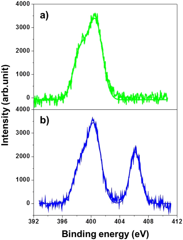
N1s XPS spectra for SAM-G/Si (a) and CNT–G/Si (b).
Figure 6.
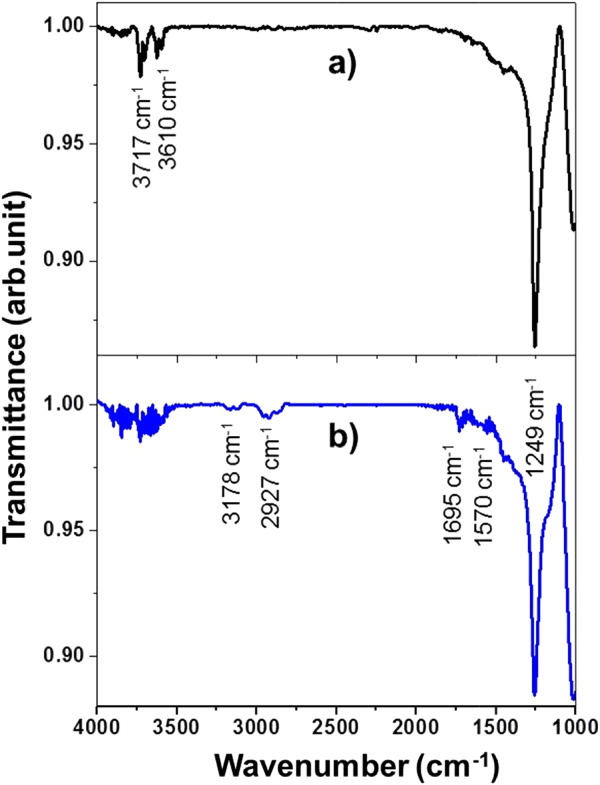
FTIR spectra for UV-G/Si (a) and CNT–G/Si (b) (note: G/Si was as a reference).
Hybrid structural characterization
The surface morphology of the hybrid material is shown in figure 7. AFM and SEM images illustrated that the CNT was homogeneously distributed onto the SAM-G/Si surface as shown in figures 7(a) and (b). To further characterize the structure of the hybrid material (CNT–G/Si), a sample was examined using TEM (figure 7). The CNT immobilized on SAM-G/Si was found to have an uninterrupted interaction between CNT and graphene, which clearly showed that CNT was anchored onto the graphene surface as shown in figures 7(c)–(f). The establishment of a uniform, continuous CNT network with graphene might be constructive for promoting hybrid properties.
Figure 7.
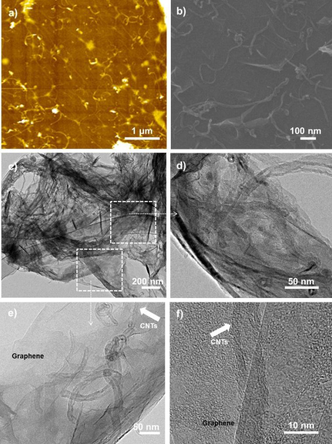
AFM and SEM images for CNT–G/Si (a and b) and TEM low and high resolution images (c–e) and (f) (arrows indicate a select region of the hybrid structure).
Field effect transistor (FET) measurement
To validate the n-type and p-type characteristics induced by the chemical binding between the CNT and graphene, FET measurements were demonstrated as shown in figure 8.
Figure 8.
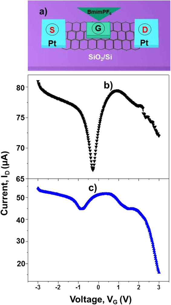
Representation of an electrochemically gate-adjusted FETs diagram (a); drain–source current versus gate voltage for G/Si (b) and CNT–G/Si (c).
Both pristine and hybrid graphene FETs were fabricated on SiO2/Si substrates using platinum for the source and drain electrodes and 1-butyl-3-methylimidazolium (BmimPF6) as an ionic liquid. The schematic procedure of FET measurements is shown in figure 8(a). The charge neutrality point for G/Si without surface treatment was around zero volts (figure 8(b)) but for CNT–G/Si, two neutrality points located at about +1.5 and −1.0 V (figure 8(c)) were indicative of sharp p–n junction behavior with energy separation of the neutrality points within complementary regions. The as-fabricated hybrid device had p-type characteristics due to adsorption of the CNT/graphene surface, while the n-type characteristic was initiated by the amide group as well as insignificant free amine groups, indicating a hybrid property from CNT–G chemical bonding.
Based upon the experimental results, the overall synthetic processes of graphene film functionalization (SAM-G/Si) and CNT immobilization onto the aforementioned surface (CNT–G/Si) are illustrated in schematic figure 1. Beyond the fabrication of an amine-terminated SAM on graphene film followed by UV-treatment, a key motivation of this work was the introduction of an active terminal group containing SAM onto CVD graphene film which could be useful to uniformly bind CNTs onto the film surface and to encourage the fabrication of other nanomaterials. Likewise, the presence of an amine group on graphene offers a greater array of potential reactions under mild surroundings; such as the binding of biomolecules, which is normally performed with amine-terminated surfaces [33]. Recently, Yung et al [44] reported a unique Pt structure decorated onto a graphene sheet. Various groups have reported that aggregation of CNT on graphene sheets leads to a loss of available surface area and a reduction in supercapacitor performance [20, 45, 46]. The results from the present study reveal a method to produce a uniform and distinctive CNT–graphene structure via covalent bonding, which might be useful in controllably preparing other graphene hybrid assemblies. Because localized SAM on graphene film can facilitate chemical patterning, an understanding of the amine–CNT interactions may offer a feasible approach to the realization of all-graphene circuits.
Conclusions
In conclusion, we have developed a simple, tunable method for the synthesis of covalently bound CNT–graphene hybrid material. UV treatment efficiently provided an effective graphene film surface on which to fabricate SAM. The amine groups on graphene promoted the adsorption of CNTs, leading to the formation of CNT–graphene hybrid material with a unique configuration. Finally, a new class of hybrid material with uniform CNT–graphene networks was demonstrated. This methodology could be of great use in the fabrication of supercapacitors, flexible hybrid electrodes, p–n junction FET devices, among other future applications.
Acknowledgments
This work was supported by the Basic Science Research Program (2012R1A1A2041021) through the National Research Foundation of Korea (NRF) funded by the Ministry of Education, Science and Technology (MEST).
References
- Novoselov K S, Geim A K, Morozov S V, Jiang D, Zhang Y, Dubonos S V I, Grigorieva V. and Firsov A A. Science. 2004;306:666. doi: 10.1126/science.1102896. [DOI] [PubMed] [Google Scholar]
- Geim A K. and Novoselov K S. Nature Mater. 2007;6:183. doi: 10.1038/nmat1849. [DOI] [PubMed] [Google Scholar]
- Lee C, Wei X D, Kysar J W. and Hone J. Science. 2008;321:385. doi: 10.1126/science.1157996. [DOI] [PubMed] [Google Scholar]
- Gilje S, Han S, Wang M, Wang K L. and Kaner R B. Nano. Lett. 2007;7:3394. doi: 10.1021/nl0717715. [DOI] [PubMed] [Google Scholar]
- Eda G, Fanchini G. and Chhowalla M. Nature Nanotechnol. 2008;3:270. doi: 10.1038/nnano.2008.83. [DOI] [PubMed] [Google Scholar]
- Rao C N R, Sood A K, Subrahmanyam K S. and Govindaraj A. Angew. Chem. Int. Edn Engl. 2009;48:7752. doi: 10.1002/anie.200901678. [DOI] [PubMed] [Google Scholar]
- Liang J, Xu Y, Huang Y, Zhang L, Wang Y, Ma Y, Li F, Guo T. and Chen Y. J. Phys. Chem. C. 2009;113:9921. [Google Scholar]
- Wang X, Zhi L J. and Mullen K. Nano Lett. 2008;8:323. doi: 10.1021/nl072838r. [DOI] [PubMed] [Google Scholar]
- Yoo E, Kim J, Hosono E, Zhou H, Kudo T. and Honma I. Nano Lett. 2008;8:2277. doi: 10.1021/nl800957b. [DOI] [PubMed] [Google Scholar]
- Leenaerts O, Partoens B. and Peeters F M. Phys. Rev. B. 2009;79:235440. [Google Scholar]
- Xu Y X. and Shi G Q. J. Mater. Chem. 2011;21:3311. [Google Scholar]
- Kodali V K, Scrimgeour J, Kim S, Hankinson J H, Carroll K M, Heer D, Berger C. and Curtis J E. Langmuir. 2011;27:863. doi: 10.1021/la1033178. [DOI] [PubMed] [Google Scholar]
- Compton O C, Dikin D A, Putz K W, Brinson L C. and Nguyen S T. Adv. Mater. 2010;22:892. doi: 10.1002/adma.200902069. [DOI] [PubMed] [Google Scholar]
- Stankovich S, Dikin D A, Compton O C, Dommett G H B, Ruoff R S. and Nguyen S T. Chem. Mater. 2010;22:4153. [Google Scholar]
- Valentini L, Cardinali M, Bon S B, Bagnis D, Verdejo R, Lopez-Manchado M A. and Kenny J M. J. Mater. Chem. 2010;20:995. [Google Scholar]
- Hossain M Z, Walsh M A. and Hersam M C. J. Am. Chem. Soc. 2010;132:15399. doi: 10.1021/ja107085n. [DOI] [PubMed] [Google Scholar]
- Liu L H, Lerner M M. and Yan M. Nano Lett. 2010;10:3754. doi: 10.1021/nl1024744. [DOI] [PMC free article] [PubMed] [Google Scholar]
- Li B, Zhiu L, Wu D, Peng H, Yan K. and Liu Z. ACS Nano. 2011;5:5957. doi: 10.1021/nn201731t. [DOI] [PubMed] [Google Scholar]
- Stine R, Ciszek J W, Barlow D E, Lee W D, Robinson J T. and Sheehan P E. Langmuir. 2012;28:7957. doi: 10.1021/la301091f. [DOI] [PubMed] [Google Scholar]
- Yu D. and Dai L. J. Phys. Chem. Lett. 2010;1:467. [Google Scholar]
- Tung V C, Chen L, Allen M J, Wassei J K, Nelson K, Kaner R B. and Yang Y. Nano Lett. 2009;9:1949. doi: 10.1021/nl9001525. [DOI] [PubMed] [Google Scholar]
- Li C Y, Li Z, Zhu H W, Wang K L, Wei J Q, Li X, Sun P, Zhang H. and Wu D. J. Phys. Chem. C. 2010;114:14008. [Google Scholar]
- Li X, Zhu Y, Cai W, Borysiak M, Han B, Chen D, Piner R D, Colombo L. and Ruoff R S. Nano Lett. 2009;9:4359. doi: 10.1021/nl902623y. [DOI] [PubMed] [Google Scholar]
- Adhikari P D, Song W, Cha M J. and Park C Y. Thin Solid Films. 2013;545:50. [Google Scholar]
- Ferrari A C. Phys. Rev. Lett. 2006;97:187401. doi: 10.1103/PhysRevLett.97.187401. [DOI] [PubMed] [Google Scholar]
- Malard L M, Pimenta M A, Dresselhaus G. and Dresselhaus M S. Phys. Rep. 2009;473:51. [Google Scholar]
- Das A, Pisana S, Chakraborty B, Piscanec S, Shah S K, Waghmare U V, Novoselov K S, Krishnamurthy H R, Geim A K. and Ferrari A C. Nature Nanotechnol. 2008;3:210. doi: 10.1038/nnano.2008.67. [DOI] [PubMed] [Google Scholar]
- Peimyoo N, Li J, Shang J, Shen X, Qiu C, Xie L, Huang W. and Yu T. ACS Nano. 2012;6:8878. doi: 10.1021/nn302876w. [DOI] [PubMed] [Google Scholar]
- Ishigami M, Chen J H, Cullen W G, Fuhrer M S. and Williams E D. Nano Lett. 2007;7:1643. doi: 10.1021/nl070613a. [DOI] [PubMed] [Google Scholar]
- Niall M, Hugo N, Nanjundan A K, Toby H. and Georg S D. Carbon. 2013;54:283. [Google Scholar]
- Rosca I D, Watari F, Uo M. and Akasaka T. Carbon. 2005;43:3124. [Google Scholar]
- Adhikari P D, Kim S, Lee S. and Park C Y. J. Nanosci. Nanotechnol. 2013;13:4587. doi: 10.1166/jnn.2013.7114. [DOI] [PubMed] [Google Scholar]
- Ramanathan T, Fisher F T, Ruoff R S. and Brinson L C. Chem. Mater. 2005;17:1290. [Google Scholar]
- Noa L, Xiaomeng S, Tatyana B, Hagai C. and Wagner H D. Carbon. 2012;50:1734. [Google Scholar]
- Adhikari P D, Tai Y, Ujihara M, Chu C C, Imae T. and Motojima S. J. Nanosci. Nanotechnol. 2010;10:833. doi: 10.1166/jnn.2010.1886. [DOI] [PubMed] [Google Scholar]
- Zhang Y, Li J, Shen Y, Ang M W. and Li J. J. Phys. Chem. B. 2004;108:15343. [Google Scholar]
- Sun Y P, Huang W, Lin Y, Fu K F, Kitaygorodskiy A, Riddle L A, Yu Y J. and Carroll D L. Chem. Mater. 2001;13:2864. [Google Scholar]
- Mou Z, Chen X, Du Y, Wang X, Yang P. and Wang S. Appl. Surf. Sci. 2011;258:1704. [Google Scholar]
- Ma Y, Sun L, Huang W, Zahang L, Zhao J, Fan Q. and Huang W. J. Phys. Chem. C. 2011;115:24592. [Google Scholar]
- Adhikari P D, Imae T. and Motojima S. Chem. Eng. J. 2011;174:693. [Google Scholar]
- Oh T. Japan. J. Appl. Phys. 2005;44:4103. [Google Scholar]
- Zhan Y, Yang X, Meng F, Wei J, Zhao R. and Liu X. J. Colloid Interface Sci. 2011;363:98. doi: 10.1016/j.jcis.2011.07.004. [DOI] [PubMed] [Google Scholar]
- Suteewong T, Sai H, Bradbury M, Estroff L A, Gruner S M. and Wiesner U. Chem. Mater. 2012;24:3895. [Google Scholar]
- Yung T Y, Lee J Y. and Liu L K. Sci. Technol. Adv. Mater. 2013;14:035001. doi: 10.1088/1468-6996/14/3/035001. [DOI] [PMC free article] [PubMed] [Google Scholar]
- Yang S Y, Chang K H, Tien H W, Lee Y F, Li S M, Wang Y S, Wang J Y, Ma C C M. and Hu C C. J. Mater. Chem. 2011;21:2374. [Google Scholar]
- Cheng Q, Tang J, Ma J, Zhang H, Shinya N. and Qin L-C. Phys. Chem. Chem. Phys. 2011;13:17615. doi: 10.1039/c1cp21910c. [DOI] [PubMed] [Google Scholar]


