Abstract
Plasmons in metallic nanomaterials exhibit very strong size and shape effects, and thus have recently gained considerable attention in nanotechnology, information technology, and life science. In this review, we overview the fundamental properties of plasmons in materials with various dimensionalities and discuss the optical functional properties of localized plasmon polaritons in nanometer-scale to atomic-scale objects. First, the pioneering works on plasmons by electron energy loss spectroscopy are briefly surveyed. Then, we discuss the effects of atomistic charge dynamics on the dispersion relation of propagating plasmon modes, such as those for planar crystal surface, atomic sheets and straight atomic wires. Finally, standing-wave plasmons, or antenna resonances of plasmon polariton, of some widely used nanometer-scale structures and atomic-scale wires (the smallest possible plasmonic building blocks) are exemplified along with their applications.
Keywords: plasmon, nanowire, nanorod, sensing, nanoparticle
Introduction
The concept of the plasmon has become increasingly important in nanotechnology in the past decade since its surface-localized mode in micron-scale objects as well as its variants in nanometer-scale objects exhibit very strong size and shape effects. Because the Fermi wavelength λF and screening length of most metals are at the nanometer scale, plasmons in metals can be tuned by changing the shape, size and dimensionality of the objects at the nanometer scale. This closely relates to the quest of nanotechnology, which is to tailor functional properties at the nanometer scale by adopting rationally designed architectures to achieve the desired functions in electronics/photonics devices [1–6]. Lithographic fabrication techniques are often used for engineering the plasmonic band dispersion of the surface plasmon polaritons and manipulating the electromagnetic field of sub-nanometer wavelengths. The dimensions of the components in such devices range from several tens to several hundred nanometers and their properties are readily predicted adopting the principles of classical electromagnetism [1–6]. On the other hand, fabrication techniques based on self-assembly, such as colloid synthesis, wet-chemical electrodeposition and molecular beam epitaxy, are also powerful methods of fabricating plasmonic materials with even smaller dimensions [8, 10, 11].
In this article, we first briefly overview the history and fundamental aspects of plasmon research by introducing some examples of electron energy loss experiments on volume plasmons, surface plasmons and recent studies on plasmons in atomic-scale metal objects. Next, we describe recent studies on optical functional properties, mostly in the infrared (IR) spectral region, of structures ranging from submicron-scale lithographically fabricated materials to atomic-scale plasmonic building blocks. In the former part, we discuss the momentum-frequency relation of prototype plasmons on smooth surfaces, in flat sheets, or in straight wires. In the latter part, we focus on optical studies of systems with various shapes and dimensions. We present results obtained from both top-down lithographically fabricated micro/nanostructures as well as bottom-up self-assembled nanoscale and atom-scale structures. For example, lithographically fabricated nanorod and nanoparticle antennas as well as gap-tuned random nanoislands have been successfully adopted to optimize the enhancement of vibrational signals by tuning the structural parameters [12–14]. Even in atom-scale metallic objects, such as atomic sheets and atomic wires, plasmons can be confined and can propagate [15–17]; moreover, they can exhibit standing-wave antenna resonance [15]. Because this research field is developing very rapidly, recent works presented here are just a few examples from a vast amount of ongoing research.
Fundamental properties of plasmons probed by electron energy loss spectroscopy
In 1941 and 1948, Ruthemann and Lang, respectively, reported the electron energy loss spectroscopy (EELS) studies of fast electrons passed through thin metal foils [18, 19]. Their pioneering works provided experimental evidence for the theory of plasma oscillation in metals proposed by Pines and Bohm in the early 1950 s [20]. While classical plasma in a high-temperature ionized gas follows Boltzmann statistics, plasma oscillation in a metal obeys Fermi statistics, and then the energy quanta of this plasma oscillation (plasmon) follow Bose–Einstein statistics [21]. A few years later, Watanabe discovered in his transmission EELS study that the energy loss of plasmon exhibits angular dependence (momentum dependence) similar to that in the Bohm–Gross relation for dilute classical plasma [22]. This was the first observation of the plasmon dispersion. For most materials, the plasmon frequency lies in the visible region and disperses at moderate rate as a function of momentum q [23]. At larger momentum values, the effect of electronic exchange correlation becomes stronger [25]. The prediction of the precise shape of the dispersion curve and its lifetime has long been an intricate problem in condensed matter physics as well as in plasma physics, and still remains a theoretical challenge [11, 26, 27].
Subsequently, in 1957, Ritchie reported a theoretical study of electron energy loss in thin films, describing surface-localized plasmon modes [28, 29]. This prediction was experimentally proven a few years later by Powell and Swan using reflection EELS, which pioneered the experimental research on surface plasmons [30]. Later, the dispersion of surface plasmons was also studied by optical spectroscopy. In 1967, Teng and Stern determined the dispersion curve by an optical method using a metallic grating structure [31], and in 1968, Otto, and then Kretschmann and Raether proposed a method for exciting plasmons using attenuated total reflection (ATR) [32, 33].
Optical and electron spectroscopy methods differently probe the plasmon dispersion curve. In contrast to the plasmon resonance in finite-size systems, propagating modes of plasmons in infinitely large/wide systems cannot be excited directly by free-space photons but can be excited by charged particles such as electrons. As shown on the left of figure 1(b), the dispersion curve follows that of the surface plasmon polariton, then gradually deviates from this straight line, and assumes the pure plasmonic property without coupling to light. Since the propagation wavelength of the excited plasmon decreases at larger q values, the quantum mechanical nature of the oscillating electrons becomes more and more apparent at larger q. Some examples of this are given below.
Figure 1.
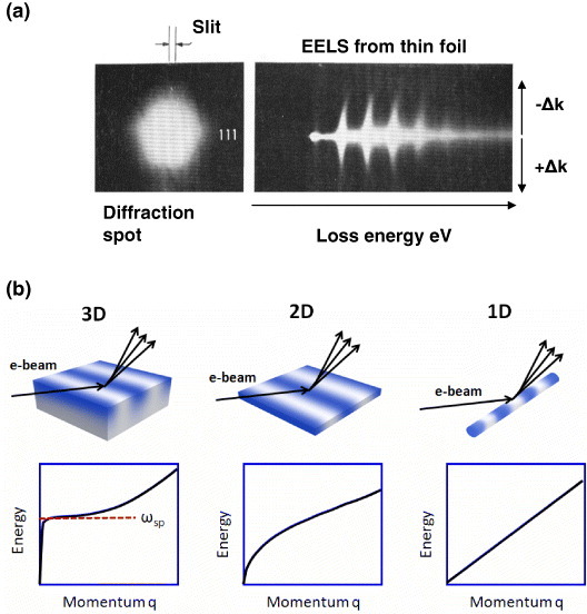
(a) The first observation of a plasmon dispersion curve by Watanabe using Möllenstedt-type EELS in 1955 [22]. Part of the electron beam at a diffraction spot was selected using a slit (left) and guided to an analyzer to construct a momentum-energy diagram on the final screen (right). (b) Schematic diagrams of electron scattering from metals with different dimensionalities and the corresponding dispersion curves (see text). ωsp denotes the energy of the surface plasma frequency.
According to the classical electromagnetism, the induced charge of a plasmon must be distributed similarly to a delta function in the surface normal direction. However, real metal surfaces consist of atoms and the electronic wave function spreads out into the vacuum at the angstrom scale. This quantum mechanical effect is known to determine the dispersion curve of surface plasmon, that is, position of the charge (center of gravity of the induced charge in the surface-normal direction) induced by the external field largely affects the slope and the polarity of the dispersion curve of the surface plasmon [34, 35]. For simple s-electron metals such as Na and K, the induced charge is located outside the metal surface and the dispersion curve exhibits a negative slope in the long-wavelength limit. For d-electron metals, the induced charge is located inside the metal surface and exhibits a positive slope [36, 37].
One example of a d-electron metal surface, the Ag(111) surface, is shown in figure 2. Here the position of the centroid of the induced charge is intentionally tuned by covering the surface with an element having a strong electron affinity [38]. When the Ag(111) surface is clean, the dispersion curve exhibits positive slope, because the induced charge is located inside the surface, owing to the s–d nature of the surface electronic wave function of Ag. However, when the surface is covered with Cl, the polarity of the initial slope is inverted and the plasmon energy exhibits large redshift. This is due to the fact that the electronic charge distribution is shifted toward the vacuum because of the charge transfer between Ag and Cl. In addition to this charge redistribution effect, the dielectric screening of the surface plasmon induced by the Cl overlayer is also responsible for the substantial redshift of the surface-plasma frequency ωsp near q=0.
Figure 2.
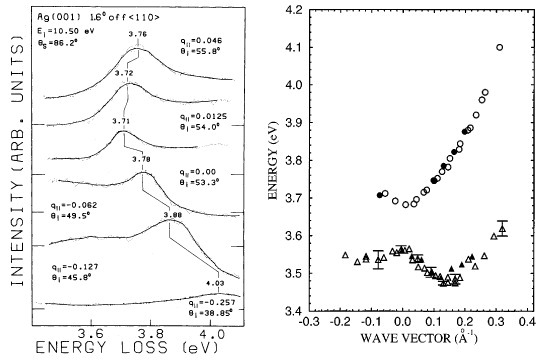
Left: an example of angle-resolved electron energy loss spectra of the clean Ag(001) surface. The incident electron energy is 10.5 eV. The energy of the surface plasmon is minimum at zero momentum and disperses to higher values as momentum q increases. (Reproduced from [36]) Right: comparison of surface-plasmon dispersion curves for the clean Ag(111) and chlorine-adsorbed Ag (111) surfaces obtained at low (<20 eV; open symbols) and high (>75 eV; shaded symbols) impact energies. Error bars are indicated for representative q vectors. (Reproduced from [38].)
Although the surface plasmon is a localized mode at the 2D surface of a crystal, its charge density oscillation soaks significantly into the inside of the 3D volume (see figure 1(b), left) and hence its surface-plasma frequency ωsp near q=0 is determined by the bulk properties. In this sense, the surface plasmon is classified as a 3D-type plasmon and its frequency lies in the same range as that of the volume plasmon. On the other hand, when the plasmon is confined in a film with a thickness markedly below the screening length of the metal and close to its Fermi wavelength, the plasmon dispersion curve dramatically changes from that of the surface plasmon. This case is shown in the middle of figure 1(b): the frequency increases from zero following √q-law, and then increases almost linearly at large q values. This behavior at a larger q is a consequence of the nonlocal nature of the electromagnetic response of this 2D system. Experimentally, such behavior has been observed for a monatomic layer of Ag on a Si substrate and explained by nearly free-electron theory based on the random phase approximation [39, 40]. Here, simple classical electromagnetism adopting the bulk Ag dielectric function and its film thickness d∼0.3 nm does not account for the entire dispersion curve because the atomic structure of the Ag monolayer is not the same as that of the Ag(111) plane of bulk Ag. Since the supporting medium of plasmon is an inherent 2D system (there is no top or bottom surface) and there is no subband in the electronic band, only one intraband 2D plasmon mode is possible in such a system. Such a plasmon is also possible in a doped graphene where the metallic band near the Dirac point is responsible for the intraband plasmonic excitations [41, 42].
In a 1D structure, as shown in the right of figure 1(b), the plasmon dispersion function is a nearly straight line (for an isolated wire or when the interaction between the wires is negligible). This sound-wave-like dispersion was introduced in the early theory of 1D electron systems by Tomonaga in 1950 [43] and some further theoretical works were subsequently carried out [44,45]. Even for a metallic atomic wire as thin as 0.3 nm, this mode can be detected by EELS [46, 47]. The atomic structure of a self-assembled chain of gold atoms is shown on the left of figure 3, and EELS spectra taken at different values of momentum q (along the chains) are presented on the right. A monotonically increasing sound-wave-like dispersion is clearly seen, as expected. The theoretical fit to the dispersion curve using a quantum-mechanical scheme that takes into account dynamic exchange-correlation effects, allows to characterize microscopic properties such as the exchange correlation effect and spin–orbit interaction. The former is a consequence of confined dynamical motion of the electrons in an atomically narrow space, even narrower than the size of the exchange-correlation hole diameter of the electrons. The latter is a consequence of the relativistic effects at the ionic cores of gold [46, 47].
Figure 3.
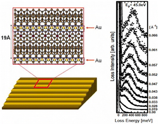
Left: atomic structure of self-assembled atomic chains of gold on a 1D template substrate (the high-index Si(557) surface). The chain width is nearly one atom (3 Å) and the chain spacing is 19 Å. Right: EELS spectra taken at different values of momentum for the incident electron energy of 45 eV. A monotonically increasing sound-wave-like dispersion is clearly observed.
In a 2D electron system screened significantly by a metallic substrate, such as a metallic surface state formed on a metal substrate, the plasmon dispersion is predicted to assume features close to those of a 2D plasmon, but its dispersion is linear in the small-momentum-energy region [48]. As shown in figure 4, the dispersion curve resembles that of the 1D plasmon but its origin is rather different [16, 17, 46, 47]. The linear dispersion is a consequence of the redshift from the 2D plasmon at larger wavenumbers owing to the increased dynamical screening from the metallic substrate [49]. In a sense, this can be regarded as an intermediate case between a surface plasmon (a 3D edge mode) and a sheer 2D plasmon. Owing to the characteristics of its dispersion curve, this mode is called the acoustic surface plasmon mode [48]. The mixed 2D–3D nature of this collective electronic excitation is reflected in the corresponding charge density nind(z) distribution, an imaginary part of which is presented on the right panel of figure 4. Here one can see how the positive regions in nind(z) corresponding to the acoustic surface plasmon closely follow to the maxima in the charge density of the surface state (an example of a 2D electron gas) at the Be(0001) surface, whereas the regions of negative charge correspond to its nodes, i.e. the regions where bulk electrons (3D electron gas) attempt to screen the charge disbalance in the 2D system. The observation of this mode by EELS was first reported for the Be(0001) surface [51] and later for Au(111) [53] and Cu(111) surfaces [54].
Figure 4.
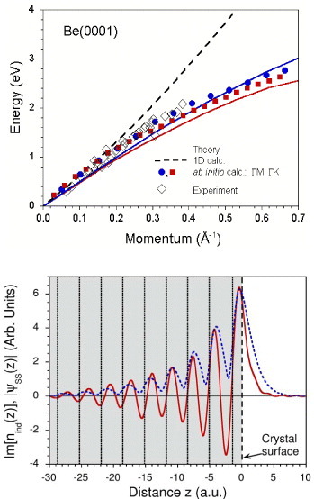
Left: ab initio acoustic surface plasmon dispersion curve for the Be(0001) surface and two different directions [51]. Dots represent the theoretical data and the open diamonds the experimental results. Solid lines delimit the upper borders of the corresponding regions for intraband electron-hole excitations within the s-pz Be(0001) surface state [52]. Dashed line shows an early dispersion prediction obtained in a simplified 1D calculation [48]. The shape of the dispersion curve is similar to that of the 1D plasmon but its origin is different [16, 17, 46, 47]. Right: imaginary part of induced charge-density distribution (red solid line) corresponding to the acoustic surface plasmon in direction perpendicular to the Be(0001) surface (ab initio calculation). Vertical lines show the atomic layer positions. Dashed line demonstrates the charge density corresponding to the Be(0001) surface states.
Optical applications of localized surface plasmon: properties of lithographic nanoarchitectures for antenna sensing
The optical properties of metallic nanostructures are of great interest owing to the extraordinarily high electromagnetic field enhancement that can be achieved upon resonant excitation with light [1–14, 55, 56]. This phenomenon originates from the surface plasmon polaritons localized at the surface of the nanostructure. In 1899, Sommerfeld discussed the propagation of electromagnetic waves on a metal cylinder [57], more than half a century before the work on thin films by Ritchie. When the cylinder has a finite length, the electromagnetic wave (plasmon) at a certain propagation wavelength can be confined and form a standing wave, which exhibits strong resonance with external field at a certain wavelength. This standing wave is classified as the so-called localized surface plasmon. The primary difference from the propagating plasmon is that this localized plasmon causes strong electromagnetic field enhancement and enables optical detection. Because of this, the properties of localized surface plasmon have been extensively studied by optical spectroscopy and widely utilized for sensing as well as for photonic applications. For a spherical metal nanoparticle, the localized plasmon resonance frequency lies in the ultraviolet to visible range. On the contrary, for elongated particles (disks, rods, etc), the localized plasmon resonance splits into two modes and the lower mode undergoes a redshift with increasing aspect ratio of the object. With appropriate geometrical parameters, it is possible to redshift the resonance frequency even into the IR region while the higher-frequency mode remains in the visible wavelength range [8, 58, 59]. The former has polarization parallel to the long axis of the particle and is called longitudinal localized surface plasmon (longitudinal mode), whereas the latter has polarization perpendicular to the long axis and is called transverse localized surface plasmon (transversal mode).
It is known that a simple nanorod with a micrometer to nanometer length provides very strong antenna resonance in the IR region by forming a standing-wave localized surface plasmon [12, 58–61]. In the following, we briefly overview some examples of nanorod antenna resonance and its applications. We focus on two topics from recent nanoantenna research: detection of phonon-polaritons in thin films and the interaction between nanoantennas in an array [12].
Gold nanorod arrays were fabricated on silicon wafers covered with a native oxide layer by electron beam lithography. The nanorods, having rectangular cross sections (width w and height h of approximately 100 nm), were arranged in regular arrays with fixed separation distances parallel (gx) and perpendicular (gy) to the long axis of the nanorods. The length L of the rods was almost constant in each array, and several arrays with different L were prepared.
Owing to the circular shape of the aperture with a diameter of 33 μm used in our IR microscope (Bruker, Hyperion 2000), approximately 27 nanorods contributed to the measured IR extinction. Dipole-like fundamental antenna resonance was clearly observed for parallel polarization (see figure 5). In addition, the sharp feature at approximately 1230 cm−1 originates from the excitation of a phonon-polariton in the thin silicon dioxide layer. This sharp feature overlaps with the contribution from antenna resonance and assumes an asymmetric Fano resonance shape, indicating that the strong hybridization takes place between the plasmon polaritons and the phonon polariton. Since no signal of the phonon-polariton is observed in perpendicular polarization, this is a proof that light scattering by the antennas is responsible for the enhanced signal from the silicon dioxide layer. Nanoantennas are therefore suitable for the surface-enhanced IR sensing of ultrathin surface layers [60].
Figure 5.
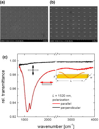
(a, b) SEM images of the fabricated nanorod arrays. (c) Relative transmittance spectra of individual nanorods in an array with gx=gy=5 μm at two different polarizations of the incident light: parallel (red curve) and perpendicular (black curve) to the long axis of the nanorods. The width and height of the nanorods are 100 nm. At 1230 cm−1, asymmetric Fano resonance feature appears due to the hybridization between plasmon polaritons of the Au nanoantenna and phonon polaritons of the thin (3 nm) dielectric layer between Si and Au.
Another branch of our research is to investigate the effects of interactions in nanorod arrays. Unequal distances gx lead to dissimilar extinction (see figure 6). The fundamental antenna resonances differ in intensity and resonance frequency. For a small gap of gx≈ 40 nm (green curve), a shift of the resonance to a smaller wavenumber is observed that can be explained by the strong interaction between the nanorods. Since most high-sensitivity sensor chips are based on densely packed plasmonic nanostructures, it is important to clarify the dependence of their performance on the geometrical arrangement and the distances between the structures. Such knowledge will help optimizing the performance of plasmonic sensors, such as those used for surface-enhanced IR absorption spectroscopy (SEIRA).
Figure 6.
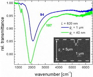
Relative transmittance spectra of two different nanorod arrays with similar dimensions but different gx as indicated in the inset.
Along with SEIRA, surface-enhanced Raman scattering (SERS) has attracted much interest in the past decades. For example, it can be used in multiplex in vivo cancer-targeting agents [62–64] because of their sharp spectroscopic fingerprint [63, 64], negligible long-term toxicity [64], and potential use in photothermal therapy [66]. In this biomedical application, plasmonic nanostructures are essential for increasing the Raman scattering efficiency, primarily caused by the local electromagnetic field enhancement [11] within the surface plasmon polariton mechanism, as in the case of SEIRA. To increase the laser penetration depth in a biological tissue, resonant excitation is required in the spectral window between red and IR, where the absorption by water and hemoglobin is minimal [65]. This is also possible when using Au nanorod array, not only with fundamental antenna-like surface modes but also with higher-order modes [66]. The correlation between the higher-order resonant modes and the Raman intensity was discussed previously [69].
Apart from nanorod antenna, one can also design and fabricate various SERS nanostructures with electron beam lithography. More complex artificial nanoparticle arrays for in vivo analysis can be realized with scanning confocal Raman microscopy. As shown in figure 7(a), for example, specially shaped nanoparticles can be designed for effective electromagnetic field enhancement at the perimeter of the nanostructures. SERS spectra shown in figure 7(c) were obtained from the two different types of Au nanoparticles from figures 7(a) and (b) with 785 nm laser excitation; these spectra demonstrate that the SERS signal can be enhanced by changing the size and the shape of the nanoparticle structures. For these particular structures, the size and shape are matched to the resonance in the IR to visible region. Systematic studies are needed on manipulating SERS properties by adopting top-down fabrication method. An illustration of multiplex cancer targeting by SERS nanoparticles encoded by Raman molecules and cancer antibodies is shown in figure 7(d).
Figure 7.
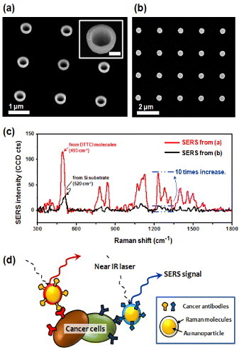
(a,b) SEM images of nanoparticles fabricated for SERS by electron-beam lithography. The scale bar in the inset corresponds to 200 nm. Images were taken at the angles of (a) 40° and (b) 0° from the surface normal. (c) Raman spectra (baseline subtracted) from the two types of Au nanoparticles in (a) and (b), which were treated with 3,3-diethylthiatricarbocyanine iodide (DTTCI) molecules. (d) Schematic illustration of multiplex cancer targeting by SERS nanoparticles encoded by Raman molecules and cancer antibodies.
Optical application of localized surface plasmon: random nanogap antenna for enhanced IR spectroscopy
In contrast to the well-defined plasmonic architectures described above, ensembles of randomly distributed nanoparticles and agglomerates can provide important optical functions such as increasing the light absorption in thin-film solar cells [70]. Also, nanofilms with a random morphology and high surface roughness provide extremely high enhancement of optical absorption by molecular vibrations in a broad spectral range [13, 14, 71–74]. This phenomenon has been known since the discovery of SEIRA in the early 1980s and has recently achieved worldwide success because the broadband plasmon resonance matches the absorption band of the molecular analytes. Vacuum deposition is a conventional preparation method of these analytes, although wet-chemical deposition has recently been developed as a quick and inexpensive method for fabricating high-sensitivity SEIRA films [13, 14, 75]. These films are more convenient for enhanced vibrational spectroscopy compared with chip-based sensor devices fabricated by lithography. However, unlike the well-defined lithographically fabricated systems, the optimization process of the enhancement factor and reproducibility are still unsatisfactory owing to the complexity and randomness of the film structure and the lack of a quantitatively controllable growth method. It is still a challenge to fully clarify the origin of the high signal enhancement and broadness in the active spectral range for these systems in relation to the nanometer-scale structural properties of the film.
The SEIRA intensity is changed markedly by a slight difference in the film preparation conditions, especially near the connection of the island films or near the percolation threshold of the islands. Therefore, it is advantageous to adopt in situ spectral monitoring during the film growth to examine the SEIRA activity at each stage of the growth.
Figures 8(a)–(c) schematically illustrate the growth of a nanogap-tuned island film at a water–Si interface for use as a SEIRA-active substrate. First, the nanoparticles are adsorbed and immobilized onto an aminosilane-treated substrate via Langmuir kinetics to form a submonolayer-saturated film [76–78]. Then gold nanoparticles are produced by electroless deposition [13, 14]. As the islands grow, they interconnect and spread laterally. Figure 8(d) shows in situ attenuated total-reflection IR spectra obtained from the growing film. Absorption from the OH stretching band of water rapidly increases as the particle size increases. As the growth proceeds, the baseline slope in the IR spectrum changes dramatically, indicating increased optical absorption extending into the IR region. Meanwhile, the OH stretching band exhibits an asymmetric Fano resonance-like feature as the film becomes percolated. From the repeated ex situ scanning electron microscopy (SEM) observations, we concluded that the baseline shift is due to the initial connection of individual nanoparticles. The asymmetric Fano shape corresponds to the percolation threshold of the islands, where the largest spectral change is assigned to the drastic change in the topology due to merging of the islands. The actual evolution of the film nanostructure is shown in figures 9(a)–(c). Image (a) corresponds to spectrum (A) in figure 8(d), and image (b) relates to spectrum (B) recorded just before percolation, when the SEIRA effect was the strongest (see figure 10(a)). Image (c) was obtained shortly after the percolation and exhibits a slight decrease in the SEIRA enhancement.
Figure 8.
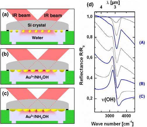
(a–c) Schematic illustration of a nanogap Au island film grown at a water–Si interface for use as a SEIRA-active substrate; (d) in situ attenuated total-reflection IR spectra obtained from the growing film. The OH stretching band of water strengthens as the particle size increases and distorts into a Fano resonance-like feature as the film becomes percolated.
Figure 9.
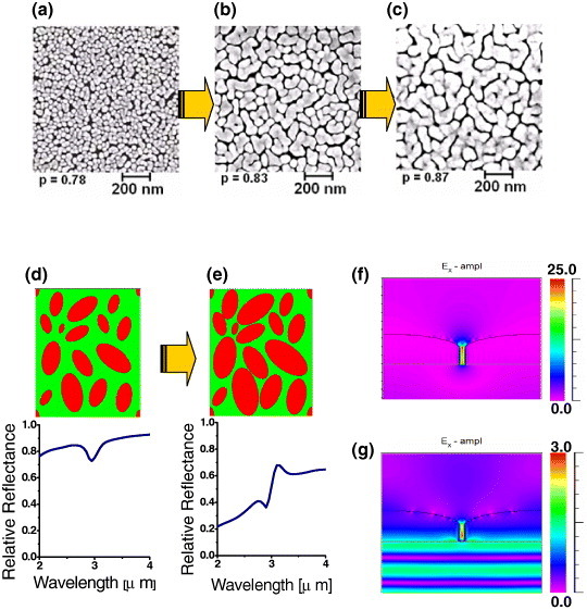
(a–c) SEM micrographs of the nanogap Au island film at different growth stages; p denotes the two-dimensional filling factor of the film. (d) A model of randomly distributed islands (red ellipsoids) at the Si–water interface (220×260 nm) and its simulated reflectance spectrum. An enhanced absorption signal from the OH stretching band of water is successfully reproduced in this electromagnetic simulation. (e) A model of grown Au islands and its simulated spectrum. The simulated water absorption signal becomes asymmetric with the decrease in the average gap between the islands. (f) Simulated electric field intensity Ex (parallel to the film) near the Au nanogap (15 nm gap) upon IR illumination (wavelength 3 μm). (g) Simulated electric field intensity Ex upon visible illumination (wavelength 550 nm). The color scale shows the field intensity normalized to the incident field value.
Figure 10.
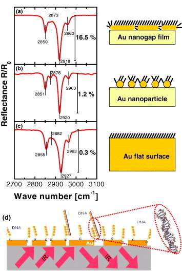
(a) IR reflectance spectrum taken from the nearly percolated Au island film. (b) Spectrum from the Au nanoparticle film before the growth. (c) Spectrum from the flat Au film. (d) Schematic illustration of a possible biosensing application.
A numerical electromagnetic simulation of the Au nanostructures was performed to determine the origin of the observed spectral change near the percolation threshold. To reproduce the observed spectral features, some key features of the island films in the SEM images were imitated to produce the model structure. The analysis was based on a rigorous coupled wave analysis (RCWA) method and could incorporate details of the structures at the nanometer scale. This is an advantage over effective medium theory, which has frequently been adopted for this type of random system. We used a Lorentz–Drude type dielectric function for Au islands. To simulate the oscillators from water molecules, we took the experimental bulk water dielectric function from W. Theiss, SCOUT Software.
As shown in figure 9(d), the simulated relative reflectance spectrum from the small islands exhibits the OH stretching band originating from the water around the Au islands. Here, the reference spectrum is that of a submonolayer of Au nanoparticles with a cylindrical shape that corresponds to the film before its growth. In stage (e), when the average gap between the islands is a few tens of nanometers, the water absorption signal becomes asymmetric. This asymmetric line shape is likely caused by the strong resonance between the OH vibration and the electronic excitation of the Au islands induced by the enhanced electromagnetic field at the ‘nanogaps’. Another reason is that the broadened plasmon resonance of the near-percolated islands undergoes a redshift toward the OH band owing to the ‘mechanical’ as well as ‘electromagnetic’ connection of the islands. Such structural features are regarded as contributing to the asymmetric shape of the OH band.
Note that this nanogap island film exhibits a rather high electric field at the gaps for incident IR light. Figure 9(f) shows the simulated electric field intensity Ex (parallel to the film) near a typical Au nanogap (15 nm gap) upon IR illumination (wavelength 3 μm). The electric field is enhanced by a factor of 25 relative to the incident beam, resulting in an approximately 625-fold enhancement in the IR signal intensity. On the other hand, the simulated electric field intensity Ex upon visible illumination (550 nm) is only three times that of the incident beam, indicating that such films are not suitable for visible-light excitation. As shown in figure 10(a), the absorption intensity from a single monolayer of octadecanthiol is high as 16.5% for a near-percolated Au film. This value is one order of magnitude larger than that of the spherical Au nanoparticles and two orders of magnitude larger than that of the flat Au surface [13, 14].
Future perspectives: standing-wave localized plasmons in an atomic-scale metallic object
As mentioned in section 2, the thinnest media known to support plasmon so far are Au atomic wires self-assembled on a stepped silicon surface [46, 47]. The same type of plasmons was recently found in some other atomic-wire systems [79–82], and two-dimensional plasmon (sheet plasmon) was also reported [39–42].
It is challenging to detect plasmonic excitation by optical spectroscopy. Compared with slow electron beams, light–matter interaction is regarded as being weaker than electron–matter interaction, and therefore photons appear to be less suitable for probing atomic-scale objects. However, for metallic systems, IR spectroscopy has proven to be a powerful method for sensitively detecting the Drude response in nanometer-thick films [83, 84]. Optical characterization of atomic-scale systems should make a breakthrough in the photonic/plasmonic research. As a first attempt, we briefly report our recent result on the optical spectroscopic characterization of plasmon in atomic-scale indium wires.
The experiments were conducted in an ultrahigh vacuum (UHV) chamber connected to a nitrogen-purged Fourier transform IR spectrometer (Nicolet-Japan, NEXUS670). Indium wires were self-assembled onto a stepped Si(111) surface (with a miscut angle of 0.9° towards the  direction). The substrate temperature was maintained at 350 °C during the deposition and the crystallinity of the indium wire array was monitored by reflection high-energy electron diffraction (RHEED). Figure 11 shows a schematic view of the wire array together with a scanning tunneling microscopy (STM) image and the atomic structure model of the indium wires (see [15, 85] and references therein).
Figure 11.
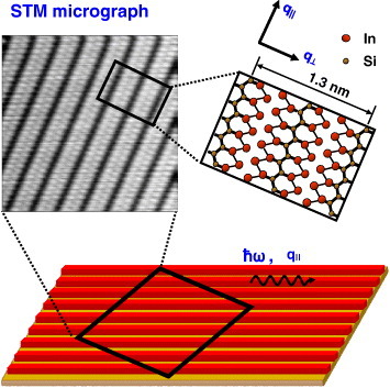
Schematic illustrations and STM image of indium atomic wires self-assembled on a Si surface. Indium wires (or indium nanobelts) have a width of approximately 1 nm and are arrayed with a 1.3 nm periodicity. Owing to the template effect of the vicinal wafer, these indium wires were aligned along the step direction. The upper right diagram shows the atomic structure proposed for this system [15].
Optical measurements were performed at room temperature, in transmittance geometry, at normal incidence and 8 cm−1 resolution, with a polarizer used for either parallel or perpendicular excitation of the electric field with respect to the atomic chains. As the thickness of the indium wires is much smaller than the IR wavelength, the light attenuation by the indium structure is proportional to its dynamic conductivity or, simply put, to the absorption by the indium chains. The IR beam had a diameter of 4 mm and probed an area of uniform distribution of the indium structures. Relative spectra were obtained by dividing the spectra of the indium wire on Si by the spectrum of the clean Si(111)-7×7 substrate (measured before indium deposition).
Figure 12(a) shows the (relative) room-temperature transmittance spectra for different polarizations and different wire crystallinities (wire lengths). Because of the anisotropy of the conductivity of the indium wires, there is a strong absorption of the electric field in the chain direction (polarization parallel to the wire). In contrast, for perpendicular polarization, the system remains almost transparent in the same frequency range. Because of the low energy and strong anisotropy, the observed feature must be related to the 1D metallic character of the indium wires [79, 82, 85]. For polarization parallel to the chains, a Drude-type metallic tail from the low frequencies to the visible range is predicted. However, we unexpectedly observed a broad resonance-like absorption signal, as was previously seen for lithographically prepared Au nanoantennas (see section 2, figures 5 and 6). The resonance is centered at ∼0.2 eV and the spectra exhibit vanishing absorption at lower wavenumbers. This feature is very similar to that observed for Au nanorods, but the dimensions of the indium wires are smaller by three orders of magnitude.
Figure 12.
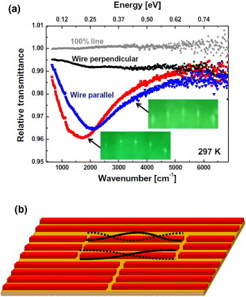
(a) IR transmittance with electrical field polarized parallel (red squares and blue triangles) and perpendicular (black circles) to the indium atomic wires. The measurements were performed for two differently prepared samples. The 100% line (gray triangles) reveals the stability of the measurement system immediately before the experiment. (b) Schematic illustration of the finite-length indium atomic wires. The wires are segmented by domain boundaries and 1D plasmons are confined to form standing wave resonating modes. Dotted and solid curves schematically illustrate the standing wave 1D plasmons. (Only the fundamental mode is observed and the overtones are not identified in our study.)
The observed feature is associated with low-energy plasmonic excitation in atomic wires [16, 46, 47, 79, 80, 86]. For sufficiently long indium wires, the plasmon frequency undergoes a redshift as the plasmon wavelength λ increases or the plasmon momentum parallel to the wire axis q∥=π/λ decreases. (Here, λ is the propagation wavelength of the plasmonic charge-density wave in the wire.) This was also observed in previous momentum-resolved EELS experiments [79, 82, 86]. For a finite wire with length L, plasmonic excitation with wavelength λ longer than 2L is not possible and the plasmon frequency remain the same as that for λ=2L=2π/q∥; it forms a standing wave, enabling optical detection. This gives the resonant IR peak at the plasmon energy for q∥≈π/L in the plasmon dispersion curve [15, 79].
Further evidence for the predicted relationship between indium chain length L and IR resonance is obtained from spectral measurements on atomic wires of different lengths. As the wire crystallinity decreases, the resonance energy increases. This can be seen in figure 12(a), where two samples with different crystallinities exhibit different resonance frequencies. The indium wires with sharper RHEED spots exhibit a lower resonance frequency (about 0.21 eV) and the indium wires with broader RHEED spots exhibit a higher resonance frequency (about 0.26 eV). This frequency difference approximately corresponds to the change in the wire length from 55 to 48 nm, referring to the plasmon dispersion curve obtained by EELS [79]. These assignments are based on the fundamental plasmons and the overtone plasmons are not observed in our experiment, possibly due to the insufficient sensitivity. The above results clearly demonstrate that the frequency of plasmons can be tuned by confining them in atomic-scale objects. Plasmonic waveguides and plasmonic resonators using these distinctive optical properties might become building blocks in future nanophotonics and sensor devices.
Conclusions
We have briefly overviewed the history and fundamental aspects of propagating plasmons as probed by EELS and discussed the functionality of localized plasmons for optical spectroscopy. Firstly, the plasmon dispersion was discussed in relation to the sub-angstrom spatial distribution of the surface-induced charge, the atomic-scale confinement of the plasmon and the substrate dynamical screening effect. Secondly, standing wave localized plasmons with micrometer to sub-micrometer lithographically prepared nanostructures were discussed. Such materials can be used for antenna sensing in the near- to mid-IR region, for characterizing chemical compositions of ultrathin dielectric layers by detecting phonon-polaritons, as well as for in vivo biosensor applications. Random nanoantennas made of a near-percolated island film were also introduced as effective, broadband, high-sensitivity substrates for detecting a molecular monolayer using enhanced IR absorption spectroscopy. Finally, metallic atomic wires were briefly discussed as prospective materials for supporting plasmonic resonating modes and waveguide modes. Such atomic wires can be used as the building blocks of future plasmonic devices.
Acknowledgments
The authors were supported by the `Strategic International Cooperative Program' funded by DFG-Germany (PU193/9) and JST-Japan, and by the Grants-in-Aid for Scientific Research from the Ministry of Education, Culture, Sports, Science and Technology of Japan. The Au nanostructures presented here were fabricated at MANA Foundry Station with the help of A Ohi.
References
- Halperin W P. Rev. Mod. Phys. 1986;58:533. doi: 10.1103/RevModPhys.58.533. [DOI] [Google Scholar]
- Atwater H A. Sci. Am. 2007;296:56. doi: 10.1038/scientificamerican0407-56. [DOI] [PubMed] [Google Scholar]
- Cao L. and Brongersma M. Nat. Photonics. 2009;3:12. doi: 10.1038/nphoton.2008.259. [DOI] [Google Scholar]
- Barnes W L, Dereux A. and Ebbesen T W. Nature. 2003;424:824. doi: 10.1038/nature01937. [DOI] [PubMed] [Google Scholar]
- Prodan E, Radloff C, Halas N J. and Nordlander P. Science. 2003;302:419. doi: 10.1126/science.1089171. [DOI] [PubMed] [Google Scholar]
- Zhang X. and Liu Z. Nat. Mater. 2008;7:435. doi: 10.1038/nmat2141. [DOI] [PubMed] [Google Scholar]
- Kreibig U. and Vollmer M. Optical Properties of Metal Clusters. Berlin: Springer; 1995. [Google Scholar]
- Link S and El-Sayed M A. 1999. J. Phys. Chem. B 103 8410 10.1021/jp9917648 [DOI] [Google Scholar]
- Novotny L. and Hecht B. Principles of Nano-Optics. Cambridge: Cambridge University Press; 2006. [Google Scholar]
- Xia Y. and Halas N J. MRS Bull. 2005;30:338. [Google Scholar]
- Moskovits M. In: Surface-Enhanced Raman Scattering. Kneipp K, , Moskovits M and Kneipp H, , editors. Berlin: Springer; 2006. p. p 1. [Google Scholar]
- Neubrech F, Weber D, Enders D, Nagao T and Pucci A. 2010. J. Phys. Chem. C 114 7299 10.1021/jp908921y [DOI] [Google Scholar]
- Enders D, Nagao T, Nakayama T. and Aono M. Japan J. Appl. Phys. 2007;49:L1222. doi: 10.1143/JJAP.46.L1222. [DOI] [Google Scholar]
- Enders D. and Nagao T. Surf. Interface Anal. 2008;40:1681. doi: 10.1002/sia.v40:13. [DOI] [Google Scholar]
- Chung H V, Kubber C J, Han G, Rigamonti S, Sanchez-Portal D, Enders D, Pucci A. and Nagao T. Appl. Phys. Lett. 2010;96:243101. doi: 10.1063/1.3451461. [DOI] [Google Scholar]
- Nagao T. Proc. SPIE. 2010;7600:76001Q-1–8. doi: 10.1117/12.841191. [DOI] [Google Scholar]
- Nagao T, Yaginuma S, Inaoka T, Nazarov V U, Nakayama T. and Aono M. Proc. SPIE. 2007;6641:664116. doi: 10.1117/12.734246. [DOI] [Google Scholar]
- Ruthemann G. Naturwissenschaften. 1941;29:648. doi: 10.1007/BF01485870. [DOI] [Google Scholar]
- Lang W. Optik. 1946;3:233. [Google Scholar]
- Pines D. and Bohm D. Phys. Rev. 1952;85:1952. [Google Scholar]
- Ichimaru S. 1986. Plasma Physics: An Introduction to Statistical Physics of Charged Particles New York: Benjamin-Cummings; chapter 7 [Google Scholar]
- Watanabe H. J. Phys. Soc. Japan. 1955;10:321. doi: 10.1143/JPSJ.10.321. [DOI] [Google Scholar]
- Raether H. Excitation of Plasmons and Interband Transitions by Electrons. Berlin: Springer; 1980. [Google Scholar]
- Egerton R F. Rep. Prog. Phys. 2009;72:016502. doi: 10.1088/0034-4885/72/1/016502. [DOI] [Google Scholar]
- vom Felde A, Sprosser-Prou J and Fink J. 1989. Phys. Rev. B 40 10181 10.1103/PhysRevB.40.10181 [DOI] [PubMed] [Google Scholar]
- Sturm K and Oliveira L E. 1981. Phys. Rev. B 24 3054 10.1103/PhysRevB.24.3054 [DOI] [Google Scholar]
- Ku W. and Eguiluz A G. Phys. Rev. Lett. 1999;82:2350. doi: 10.1103/PhysRevLett.82.2350. [DOI] [Google Scholar]
- Ritchie R. Phys. Rev. 1957;106:874. doi: 10.1103/PhysRev.106.874. [DOI] [Google Scholar]
- Ritchie R. Sur. Sci. 1973;34:1. doi: 10.1016/0039-6028(73)90183-0. [DOI] [Google Scholar]
- Powell C J. and Swan J B. Phys. Rev. 1959;115:869. doi: 10.1103/PhysRev.115.869. [DOI] [Google Scholar]
- Teng Y. and Stern E A. Phys. Rev. Lett. 1967;19:511. doi: 10.1103/PhysRevLett.19.511. [DOI] [Google Scholar]
- Otto A. Z. Phys. 1968;216:398. doi: 10.1007/BF01391532. [DOI] [Google Scholar]
- Kretschmann E and Raether H. 1968. Z. Naturforsh. A 23 2135 [Google Scholar]
- Feibelman P J. Prog. Surf. Sci. 1982;12:287. doi: 10.1016/0079-6816(82)90001-6. [DOI] [Google Scholar]
- Plummer W, Tsuei K-D and Kim B-O. 1995. Nucl. Instrum. Methods Phys. Res. B 96 448 10.1016/0168-583X(95)00311-8 [DOI] [Google Scholar]
- Rocca M. and Valbusa U. Phys. Rev. Lett. 1990;64:2398. doi: 10.1103/PhysRevLett.64.2398. [DOI] [PubMed] [Google Scholar]
- Rocca M, Biggio F and Balbusa U. 1990. Phys. Rev. B 42 2385 10.1103/PhysRevB.42.2835 [DOI] [PubMed] [Google Scholar]
- Kim J-S, Chen L, Kesmodel L L, Garcia-Gonzalez P and Liebsch A. 1997. Phys. Rev. B 56 R4402 10.1103/PhysRevB.56.R4402 [DOI] [Google Scholar]
- Nagao T, Hildebrandt T, Henzler M. and Hasegawa S. Phys. Rev. Lett. 2001;86:5747. doi: 10.1103/PhysRevLett.86.5747. [DOI] [PubMed] [Google Scholar]
- Nagao T, Hildebrandt T, Henzler M. and Hasegawa S. Surf. Sci. 2001;493:680. doi: 10.1016/S0039-6028(01)01282-1. [DOI] [PubMed] [Google Scholar]
- Nagashima A, Nuka K, Satoh K, Itoh H, Ichinokawa T, Oshima C. and Otani S. Surf. Sci. 1993;287–288:609. doi: 10.1016/0039-6028(93)91037-P. [DOI] [Google Scholar]
- Liu Yu, Willis R F, Emtsev K V and Seyller T. 2008. Phys. Rev. B 78 201403 10.1103/PhysRevB.78.201403 [DOI] [Google Scholar]
- Tomonaga S. Prog. Theor. Phys. 1950;5:544. doi: 10.1143/PTP.5.544. [DOI] [Google Scholar]
- Wendler L and Grigoryan V G. 1991. Phys. Rev. B 49 14531 10.1103/PhysRevB.49.14531 [DOI] [PubMed] [Google Scholar]
- Calmels L and Gold A. 1995. Phys. Rev. B 52 10841 10.1103/PhysRevB.52.10841 [DOI] [PubMed] [Google Scholar]
- Nagao T, Yaginuma S, Inaoka T. and Sakurai T. Phys. Rev. Lett. 2006;97:116802. doi: 10.1103/PhysRevLett.97.116802. [DOI] [PubMed] [Google Scholar]
- Nagao T, Yaginuma S, Inaoka T, Sakurai T. and Jeon D. J. Phys. Soc. Japan. 2007;76:114714. doi: 10.1143/JPSJ.76.114714. [DOI] [Google Scholar]
- Silkin V M, García-Lekue A, Pitarke J M, Chulkov E V, Zaremba E. and Echenique P M. Europhys. Lett. 2004;66:260. doi: 10.1209/epl/i2003-10184-1. [DOI] [Google Scholar]
- Pitarke J M, Nazarov V U, Silkin V M, Chulkov E V, Zaremba E and Echenique P M. 2004. Phys. Rev. B 70 205403 10.1103/PhysRevB.70.205403 [DOI] [Google Scholar]
- Silkin V M. et al 2008. Phys. Status Solidi a 205 13070 [Google Scholar]
- Diaconescu B.et al2007Nature 44857. 10.1038/nature05975 [DOI] [PubMed] [Google Scholar]
- Chulkov E V, Silkin V M. and Shirykalov E N. Surf. Sci. 1987;188:287. doi: 10.1016/S0039-6028(87)80158-9. [DOI] [Google Scholar]
- Park S J. and Palmer R E. Phys. Rev. Lett. 2010;105:016801. doi: 10.1103/PhysRevLett.105.016801. [DOI] [PubMed] [Google Scholar]
- Pohl K, Diaconescu B, Vercelli G, Vattuone L, Silkin V M, Chulkov E V, Echenique P M. and Rocca M. Europhys.Lett. 2010;90:57006. doi: 10.1209/0295-5075/90/57006. [DOI] [Google Scholar]
- Ushioda S and Sasaki Y. 1983. Phys. Rev. B 27 1401 10.1103/PhysRevB.27.1401 [DOI] [Google Scholar]
- Miyazaki H T. and Kurokawa Y. Phys. Rev. Lett. 2006;96:097401. doi: 10.1103/PhysRevLett.96.097401. [DOI] [PubMed] [Google Scholar]
- Sommerfeld A. Ann. Phys. Chem. 1899;67:233. doi: 10.1002/(ISSN)1521-3889. [DOI] [Google Scholar]
- Crozier K B, Sundaramurthy A, Kino G S. and Quate C F. J. Appl. Phys. 2003;94:4632. doi: 10.1063/1.1602956. [DOI] [Google Scholar]
- Ueno K, Mizeikis V, Juodkazis V, Sasaki K. and Misawa H. Opt. Lett. 2005;30:2158. doi: 10.1364/OL.30.002158. [DOI] [PubMed] [Google Scholar]
- Neubrech F, Pucci A, Cornelius T W, Karim S, García-Etxarri A. and Aizpurua J. Phys. Rev. Lett. 2008;101:157403. doi: 10.1103/PhysRevLett.101.157403. [DOI] [PubMed] [Google Scholar]
- Schnell M, García-Etxarri A, Huber A J, Crozier K, Aizpurua J. and Hillenbrand R. Nat. Photonics. 2009;3:287. doi: 10.1038/nphoton.2009.46. [DOI] [Google Scholar]
- Qian X, Peng X H, Ansari D O, Yin-Goen Q, Chen G Z, Shin D M, Yang L, Young A N, Wang M D. and Nie S. Nat. Biotechnol. 2008;26:83. doi: 10.1038/nbt1377. [DOI] [PubMed] [Google Scholar]
- Su X, Zhang J, Sun L, Koo T W, Chan S, Sundararajan N, Yamakawa M. and Berlin A A. Nano Lett. 2005;5:49. doi: 10.1021/nl0484088. [DOI] [PubMed] [Google Scholar]
- Keren S, Zavaleta C, Cheng Z, de la Zerda A, Gheysens O. and Gambhir S S. Proc. Natl Acad. Sci. USA. 2009;105:5844. doi: 10.1073/pnas.0710575105. [DOI] [PMC free article] [PubMed] [Google Scholar]
- Connor E E, Mwamuka J, Gole A, Murphy C J. and Wyatt M D. Small. 2005;1:325. doi: 10.1002/(ISSN)1613-6829. [DOI] [PubMed] [Google Scholar]
- Huang X, El-Sayed I H, Qian W. and El-Sayed M A. J. Am. Chem. Soc. 2006;128:2115. doi: 10.1021/ja057254a. [DOI] [PubMed] [Google Scholar]
- Mahmood U. and Weissleder R. Mol. Cancer Ther. 2003;2:489. [PubMed] [Google Scholar]
- Billot L, Lamy de la Chapelle A, Grimault A S, Vial A, Barchiesi D, Bijeon J L, Adam P M. and Royer P. Chem. Phys. Lett. 2006;422:303. doi: 10.1016/j.cplett.2006.02.041. [DOI] [Google Scholar]
- Felidj N, Laurent G, Grand J, Aubard J, Levi G, Hohenau A, Aussenegg F R. and Krenn J R. Plasmonics. 2006;1:39. doi: 10.1007/s11468-005-9004-1. [DOI] [Google Scholar]
- Catchpole K R. and Polman A. Opt. Express. 2008;16:21793. doi: 10.1364/OE.16.021793. [DOI] [PubMed] [Google Scholar]
- Hartstein A, Kirtley J R. and Tang J C. Phys. Rev. Lett. 1980;45:201. doi: 10.1103/PhysRevLett.45.201. [DOI] [Google Scholar]
- Hatta A, Ohshima T and Suetaka W. 1982. Appl. Phys. A 29 71 10.1007/BF00632429 [DOI] [Google Scholar]
- Osawa M. Chem. Soc. Japan. 1997;70:2861. doi: 10.1246/bcsj.70.2861. [DOI] [Google Scholar]
- Futamata M. 2001. J. Phys. Chem. B 105 6933 10.1021/jp010344r [DOI] [Google Scholar]
- Brown K R, Lyon L A, Fox A P, Reiss B D. and Natan M J. Chem. Mater. 2000;12:314. doi: 10.1021/cm980066h. [DOI] [Google Scholar]
- Enders D, Nagao T, Pucci A. and Nakayama T. Surf. Sci. 2006;600:L71. doi: 10.1016/j.susc.2006.01.019. [DOI] [Google Scholar]
- Enders D, Nagao T. and Nakayama T. Langmuir. 2007;23:6119. doi: 10.1021/la063239n. [DOI] [PubMed] [Google Scholar]
- Enders D, Nagao T. and Nakayama T. Japan J. Appl. Phys. 2007;46:3020. doi: 10.1143/JJAP.46.3020. [DOI] [Google Scholar]
- Liu C, Inaoka T, Yaginuma S, Nakayama T, Aono M and Nagao T. 2008. Phys. Rev. B 77 205415 10.1103/PhysRevB.77.205415 [DOI] [Google Scholar]
- Liu C, Inaoka T, Yaginuma S, Nakayama T, Aono M. and Nagao T. Nanotechnology. 2008;19:355204. doi: 10.1088/0957-4484/19/35/355204. [DOI] [PubMed] [Google Scholar]
- Rugeramigabo E P, Nagao T and Pfnür H. 2010. Phys. Rev. B 78 155402 10.1103/PhysRevB.78.155402 [DOI] [Google Scholar]
- Nagao T. Surf. Interface Anal. 2008;40:1764. doi: 10.1002/sia.v40:13. [DOI] [Google Scholar]
- Fahsold G, Priebe A, Magg N. and Pucci A. Thin Solid Films. 2003;428:107. doi: 10.1016/S0040-6090(02)01225-7. [DOI] [Google Scholar]
- Lovrinčić R and Pucci A. 2009. Phys. Rev. B 80 205404 10.1103/PhysRevB.80.205404 [DOI] [Google Scholar]
- Yeom H W.et al1999Phys. Rev. Lett. 824858. 10.1103/PhysRevLett.82.4898 [DOI] [Google Scholar]
- Hwang C G, Kim N D, Shin S Y. and Chung J W. New J. Phys. 2007;9:249. doi: 10.1088/1367-2630/9/8/249. [DOI] [Google Scholar]


