Abstract
Solution-based electrospray film deposition, which is compatible with continuous, roll-to-roll processing, is applied to chalcogenide glasses. Two chalcogenide compositions are demonstrated: Ge23Sb7S70 and As40S60, which have both been studied extensively for planar mid-infrared (mid-IR) microphotonic devices. In this approach, uniform thickness films are fabricated through the use of computer numerical controlled (CNC) motion. Chalcogenide glass (ChG) is written over the substrate by a single nozzle along a serpentine path. Films were subjected to a series of heat treatments between 100 °C and 200 °C under vacuum to drive off residual solvent and densify the films. Based on transmission Fourier transform infrared (FTIR) spectroscopy and surface roughness measurements, both compositions were found to be suitable for the fabrication of planar devices operating in the mid-IR region. Residual solvent removal was found to be much quicker for the As40S60 film as compared to Ge23Sb7S70. Based on the advantages of electrospray, direct printing of a gradient refractive index (GRIN) mid-IR transparent coating is envisioned, given the difference in refractive index of the two compositions in this study.
Keywords: Engineering, Issue 114, Electrospray, chalcogenide glasses, thin films, microphotonics, mid-infrared, gradient refractive index, physics
Introduction
Chalcogenide glasses (ChGs) are well-known for their broad infrared transmission and amenability to uniform thickness, blanket film deposition 1-3. On-chip waveguides, resonators, and other optical components can then be formed from this film by lithography techniques, and then subsequent polymer coating to fabricate microphotonic devices 4-5. One key application that we seek to develop is small, inexpensive, highly sensitive chemical sensing devices operating in the mid-IR, where many organic species have optical signatures 6. Microphotonic chemical sensors can be deployed in harsh environments, such as near nuclear reactors, where exposure to radiation (gamma and alpha) is likely. Hence an extensive study of the modification of optical properties of the ChG electrospray materials is critical and will be reported in another paper. In this article, electrospray film deposition of ChGs is exhibited, as it is a method only recently applied to ChGs 7.
The existing film deposition methods can be categorized into two classes: vapor deposition techniques, such as thermal evaporation of bulk ChG targets, and solution-derived techniques, such as by spin-coating a solution of ChG dissolved in an amine solvent. Generally, solution-derived films tend to result in higher loss of the light signal due to the presence of residual solvent in the film matrix 3, but a unique advantage of solution-derived techniques over vapor deposition is the simple incorporation of nanoparticles (e.g., quantum dots or QDs) prior to spin-coating 8-10. However, aggregation of nanoparticles has been observed in spin-coated films 10. In addition, while vapor deposition and spin-coating approaches are well-suited to the formation of uniform thickness, blanket films, they do not lend themselves well to localized depositions, or engineered non-uniform thickness films. Furthermore, scale-up of spin-coating is difficult because of high material waste due to run-off from the substrate, and because it is not a continuous process 11.
In order to overcome some of the limitations of current ChG film deposition techniques, we have investigated the application of electrospray to the ChG materials system. In this process, an aerosol spray can be formed of the ChG solution by applying a high voltage electric field 7. Because it is a continuous process which is compatible with roll-to-roll processing, near 100% use of material is possible, which is an advantage over spin-coating. In addition, we have proposed that isolation of single QDs in the individual ChG aerosol droplets could lead to better QD dispersion, due to the charged droplets being spatially self-dispersing by Coulombic repulsion, combined with the quicker drying kinetics of the high surface area droplets that minimize the movement of QDs due to the increasing viscosity of the droplets while in-flight 7, 12. Finally, localized deposition is an advantage that can be utilized to fabricate GRIN coatings. Explorations of both QD incorporation and GRIN fabrication of ChG with electrospray are currently underway to be submitted as a future article.
In this publication, the flexibility of electrospray is demonstrated by both localized depositions and uniform thickness films. To investigate the suitability of the films for planar photonic applications, transmission Fourier transform infrared (FTIR) spectroscopy, surface quality, thickness, and refractive index measurements are utilized.
Protocol
Caution: Please consult Material Safety Data Sheets (MSDS) when working with these chemicals, and be aware of the other hazards such as high voltage, mechanical motion of the deposition system, and high temperatures of the hotplate and furnaces utilized.
Note: Begin this protocol with bulk chalcogenide glass, which is prepared by well-known melt-quench techniques 2.
1. Preparation of ChG Solutions
Note: Two solutions are utilized in this study, Ge23Sb7S70 and As40S60, both dissolved in ethanolamine at a concentration of 0.05 g/ml. The preparation of the two solutions are identical. Perform all steps in this section inside of a fume hood.
Crush the bulk glass into a fine powder using a mortar and pestle.
Mix 0.25 g of the glass with 5 ml of ethanolamine solvent.
Allow 1-2 days for complete dissolution of the glass. Expedite dissolution by heating the solution on a hotplate with a surface temperature of ~50-75 °C. Increase the rate of dissolution by stirring the mixture, such as with a magnetic stirring bar.
Filter solution into a vial with 0.45 µm polytetrafluoroethylene (PTFE) filter to remove any large precipitates from the solution.
2. Setting up the Deposition Process
Note: The electrospray deposition system is depicted schematically in Figure 1. In this process, a 50 µl glass syringe with PTFE-tipped plunger is utilized. The syringe is a removable needle style with a cone-tipped, 22 gauge outer diameter needle (0.72 mm outer diameter, 0.17 mm inner diameter), and is connected to the vertically oriented syringe pump of the electrospray system. The electrospray system is exposed to ambient atmosphere in these initial experiments, though the system is set-up inside of a glovebox. The system should be set-up in a location where it is isolated from the user, such as a fume hood.
Place the end of the needle into the ChG solution. Draw the solution into the syringe by setting the syringe pump in extract mode at a slow rate, such as 150 µl/hr, to prevent the formation of bubbles.
Set the working distance (10 mm in this case) between the end of the nozzle and the top of the Si substrate by using the CNC in manual movement mode. Place the Si substrate, which is undoped and has a resistivity of 10,000 Ohm-cm, on an aluminum plate connected to the power supply ground return.
Allow a small volume of liquid to coat the outside surface of the nozzle by dispensing some liquid from the syringe utilizing the syringe pump. Turn hotplate on at a surface temperature of about 75-100 °C. Wait for ~2 hr to allow a film of glass to dry on the nozzle surface. This coating aids the stability of the spray.
3. Electrospray Deposition of ChG Films
Connect the direct current (DC) power supply to the syringe nozzle with an electrical clip.
Set flow rate at 10 µl/hr, and tune DC voltage to form a stable Taylor cone (~4 kV at 10 mm working distance). View the spray with a high magnification camera.
- Start CNC motion of the spray over the substrate to deposit film, once the spray is stable.
- Use a serpentine path for uniform thickness, or one-dimensional (1-D) passes for a linear thickness profile.
- Use passes with a distance longer than the width of the substrate, such that the spray moves completely off of the substrate before making the next pass. This is done so that the flow rate of liquid is the same at every point on the substrate.
- Control the CNC using LinuxCNC software. For an example, use the supplementary G-code for a serpentine path with 0.5 mm offset between passes, velocity of 20 mm/min, and 30 mm length of the passes. Figure 1 shows a schematic of a film made with the serpentine path and also defines the coordinate system.
Subject the deposited film to a series of heat treatments under vacuum for 1 hr each at 100, 125, 150 and 175 °C, and 16 hr at 200 °C. An optimization of the heat treatment parameters is presented in the Representative Results section of this article.
4. Characterization of the ChG Films
- Characterization of Residual Solvent Removal
- Take a transmission FTIR spectrum periodically throughout the annealing conditions, measuring the same location on the sample each time. Draw an outline of the substrate on the sample stage, and place it within this outline each time a measurement is taken.
- In the FTIR software, click "Experiment Setup," and type in the number of scans as 64. Click to the "Bench" tab and type in the scan range as 7,000 cm-1 to 500 cm-1. Take a background scan with just the sample stage in the instrument by clicking on "Collect Background." Then place the sample on the stage, and click "Collect Sample" to take the spectrum of the sample.
- To track the removal of solvent, estimate the size of the organic absorptions in the film matrix. In the FTIR software, draw a baseline in the spectral range of interest, approximately 2,300-3,600 cm-1. The software calculates the area beneath the transmission spectrum of the sample, relative to the baseline designated by the user.
- Measurement of Film Thickness
- Scratch the film with fine point tweezers, until the dark substrate becomes visible amongst the lighter colored film, which typically occurs in one scratching motion with light pressure. Remove debris caused by scratching with compressed nitrogen.
- Measure the thickness of blanket films by using a contact profilometer to determine the step height from film to substrate. Open "Measurement Setup," and type in scan rate of 0.1 mm/sec, and scan length of 500 µm.
- Place sample on stage, locating the scratch and rotating the sample such that the scratch is oriented in the left-right direction. Move the stage such that the cross-hairs are just below the scratch, and begin the surface scan by clicking "Measurement."
- Once the scan is finished, drag the R and M cursors so that they are both on the film surface, and click "Level Two Point Linear" to level the surface profile. Move one cursor to the bottom of the scratch, and write down the distance between each cursor position in the y-dimension. Measure thickness at multiple locations to obtain an average thickness and variance in the data.
- Determine the thickness profiles of the non-uniform thickness films by scanning the profilometer across the entire film (perpendicular to the 1-D motion used to deposit the film), and use this surface profile to create a graph of film thickness vs. position.
- Scan across the entire film by entering an appropriate scan length greater than the width of the film, usually 10-20 mm, in "Measurement Setup." Place the cross-hairs on uncoated substrate on one side of the film and click "Measurement," allowing the profilometer to complete the scan on uncoated substrate on the other side of the film. Right click on the surface profile and export as a .csv file.
- Alternatively, if the substrate is not flat enough to obtain reliable thickness data, scratch the film down to the substrate with about 1 mm between scratches, and scan profilometer across entire film. Write down the thickness and horizontal position at each scratch, and create a graph of film thickness vs. position from these data points.
Measure surface roughness with a white-light interferometer 13. Adjust the focus and stage tilt to generate interference fringes over the entire measurement area, which in this case was 414 µm x 414 µm using the 5x objective. Take five measurements across the uniform thickness film to determine the average roughness and variance of the data.
- Measure the refractive index with an ellipsometer 14 in the range of 600-1,700 nm wavelength. In this case, use an angle of incidence of 60°, and focus the beam to a spot size of 35 µm.
- Take a measurement on the uncoated substrate, fitting the data to determine the thickness of the native oxide layer. Use this information to model the sample as a three layer system: Si wafer + native oxide + deposited film. Take eight measurements at different locations on the sample to determine the average refractive index and variance, while using the Cauchy model to fit the data.
Representative Results
A schematic representation of the serpentine path utilized to obtain uniform thickness films with single nozzle electrospray is shown in Figure 2. Figure 3 shows an example transmission FTIR spectrum of a partially-cured As40S60 film made with serpentine motion of the spray, as well as the spectrum of pure ethanolamine solvent. From the information that can be obtained from the FTIR spectra such as shown in Figure 3, Figure 4 shows the evolution of the solvent throughout the heat treatments of uniform thickness Ge23Sb7S70 and As40S60 films. Solvent removal is a key component of solution-based ChG film processing. This is mainly because the presence of residual solvent causes absorption loss of light in the intended device operation range in the mid-IR. Therefore, the use of transmission FTIR spectroscopy is a metric that can be utilized to optimize the heat treatment conditions that lead to a minimum concentration of residual solvent, and indicates processing conditions that may lead to minimum loss of light. Film surface roughness causes scattering loss of light, so measuring this is also useful to optimize the processing conditions for minimum loss. However, it should be noted that a true loss measurement consists of coupling light into the film or waveguide fabricated from the film to allow a long path length on the order of cm. In addition to understanding loss, it is also important to understand the refractive index of the film for optical design of the device. Refractive index dispersion of the films after all heat treatments were completed is shown in Figure 5. This measurement can be analyzed through comparison of film refractive index to that of the corresponding bulk glass. The refractive index of a ChG film generally varies to some degree from the corresponding bulk glass, and this variation can be a result of differences in the structural arrangement of the atoms, compositional changes due to the deposition process or volatilization during heat treating. In the case of solution-derived films, the refractive index also changes throughout the heat treatments as solvent is removed and the film densifies.
Finally, Figure 6 shows the thickness profiles of films deposited with 1-D motion of the spray. In this case, the thickness decreases linearly from the centerline of the film. With measurements of film thickness variation, the spatial flow rate within the spray can be understood, allowing a desired structure to be engineered. Figure 7 shows photographs of the films made with serpentine and 1-D motion of the spray for reference. Generally, visual analysis of the films can be made by observing the effects of optical interference. In this two-layer, film + substrate system, regions of uniform thickness appear to be the same color (assuming that the refractive index remains constant).
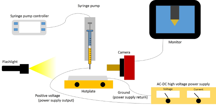 Figure 1:Schematic representation of electrospray deposition system. This schematic shows all key components to the system, with the exception of the CNC machine. Please click here to view a larger version of this figure.
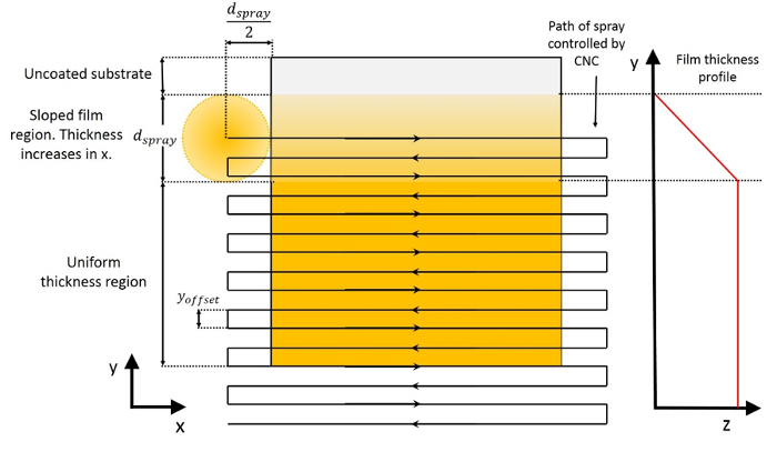 Figure 2: Schematic representation of the CNC-controlled serpentine path to obtain uniform thickness films. The spray is depicted at the beginning of the deposition, which then then traces out the path indicated by the arrows. The approximate resulting film thickness profile is shown to the right of the substrate. Please click here to view a larger version of this figure.
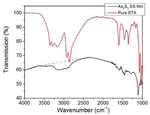 Figure 3:Comparison of infrared transmission spectra of pure ethanolamine solvent to partially cured As40S60 film. The solvent is measured with attenuated total reflection (ATR), and the film is measured in transmission through film and Si substrate. The primary spectral range of interest are the absorptions due to the presence of residual ethanolamine solvent in the film matrix at ~2,300-3,600 cm-1 wavenumber. A straight baseline is drawn in this range, and the integrated area beneath the absorptions relative to that baseline is calculated in order to track the removal of residual solvent from the film matrix. Please click here to view a larger version of this figure.
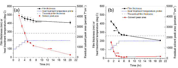 Figure 4:Plot of the integrated area beneath residual solvent absorptions. The area is taken from the range of ~2,300-3,600 cm-1 from transmission FTIR spectra of uniform thickness Ge23Sb7S70 (a) and As40S60 (b), throughout vacuum heat treatments of the samples. The temperature profile of the heat treatments is given by the dashed blue line, and the theoretical film thickness is given by the dashed gray line, which was predicted using Equation 1. The data in these figures is from sequential heat treatment and periodic characterization of the same samples. The error bars on film thickness are ± one standard deviation of the five measurements, while the error bars on solvent peak area are ± 5%, which was found to be the approximate variance of this method. Please click here to view a larger version of this figure.
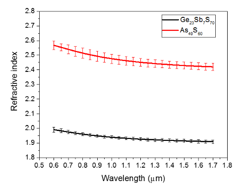 Figure 5: Refractive index of uniform thickness electrosprayed films. This data was measured by ellipsometry and fit with the Cauchy model. The Ge23Sb7S70 film was annealed for 20 hr according to Figure 3, and has a thickness of ~410 nm. The As40S60 film was also annealed for 20 hr according to Figure 4, and has a thickness of ~200 nm. The error bars are ± one standard deviation of the measurements at eight different sample locations. Please click here to view a larger version of this figure.
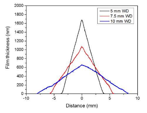 Figure 6: Thickness profiles of films made with 1-D motion of the spray, leading to linearly changing film thickness. Working distance is varied, while flow rate is fixed at 10 µl/hr, and velocity of the spray over the substrate is fixed at 1 mm/min. Please click here to view a larger version of this figure.
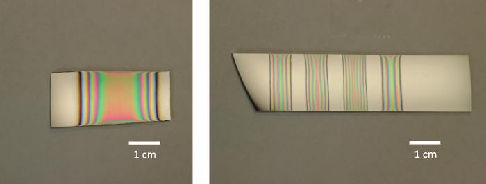 Figure 7: Photographs of films made with serpentine path (left, 10 mm working distance), and 1-D motion (right, 5 mm working distance). For the films made with 1-D motion, the number of passes was 8, 10, 12, and 6, going from left to right. Please click here to view a larger version of this figure.
Supplementary code: Example G-code utilized for serpentine path. This code allows movement of the nozzle in a serpentine path with velocity of 20 mm/min, 30 mm distance of each pass, and 0.5 mm offset between each pass. Please click here to download this file.
Discussion
At the beginning of a uniform thickness film deposited with serpentine motion of the spray relative to the substrate, the film thickness profile is increasing. Once the distance travelled in the y-direction exceeds the diameter of the spray (upon arrival at the substrate), the flow rate becomes approximately equivalent for every point on the substrate, and thickness uniformity is achieved. To determine the appropriate deposition parameters of a uniform thickness electrosprayed film, theoretical film thickness, T, is utilized. This is given by Equation 1, which is derived from the deposition parameters shown in Table 1.
![]()

In this estimation of theoretical thickness, films are assumed to be fully cured with the same density as the bulk glass, as it is ideal for the films to approach the properties of the corresponding bulk glass. Using this estimation is therefore useful in the optimization of heat treatments for solvent removal and full densification of the films, so that bulk glass properties, such as refractive index, can be approached. Solvent removal is extremely important so that the films are as transmissive as possible in the mid-IR region, as the presence of residual solvent can lead to absorption loss of light through the material. Figures 3 and 4 show the heat treatment optimizations of Ge23Sb7S70 and As40S60, respectively. Extended vacuum baking at 200 °C (the maximum temperature of the furnace) for 16 hr is necessary to minimize the size of the solvent absorption peaks in the Ge23Sb7S70 film matrix, whereas similar peak sizes are observed in the As40S60 film after ~7 hr. Likewise, it was found that As40S60 approaches theoretical thickness after ~7 hr of vacuum baking, and becomes thinner than the theoretical value with extended annealing, while Ge23Sb7S70 remains significantly thicker than the theoretical value despite extended heat treatments. If a film is thicker than the theoretical value, this likely indicates that it contains porosity and/or residual solvent. If a film is thinner than the theoretical value, the most likely explanation is that some material has volatilized, and possibly changed stoichiometry as a result, affecting the targeted optical properties. The thickness data presented are averages of five measurements over a device-relevant area of approximately 1 cm2, and the relatively small error bars on the thickness measurements confirms that the serpentine path leads to good thickness uniformity.
In addition to solvent removal, minimizing film surface roughness is also very important to minimize the loss of light through the material. It has been shown previously that surface roughness on waveguides can lead to scattering loss of light 15. The root mean squared (RMS) roughness of the Ge23Sb7S70 film after 20 hr vacuum baking was 2.5 nm ± 1.0 nm, while the RMS roughness of the As40S60 film was 5.8 nm ± 1.1 nm. The surface quality could possibly be optimized further by tuning other deposition parameters, such as working distance and flow rate. However, these initial values are acceptable for initial studies on possible use in optical devices 16.
As expected, differences were observed in the refractive indices of the two compositions studied, meaning that a GRIN could be directly "printed" by simultaneous spray of the two solutions, or by multilayer structures of the two compositions. The measured refractive indices of the two compositions studied in this article are similar to previous studies on spin-coated films of the same composition, where As40S60 approaches the index of the corresponding bulk glass, while Ge23Sb7S70 tends to remain below the index of the corresponding bulk glass 1, 17. Work is currently underway to demonstrate an effective GRIN coating through the deposition of multilayer films, where the individual compositions have a linear change in the film thickness. A linearly changing film thickness, or triangular shaped film cross-section, can be obtained with 1-D motion of the spray over the substrate. The coverage area of the coating can be tuned by varying working distance, while the slope of the film thickness can be tuned by varying the number of passes or velocity of the pass.
Electrospray is capable of continuous manufacturing 18, which is a potential advantage for scale-up compared to more traditional spin-coating and thermal evaporation of ChG films, which are discrete in nature. In addition, engineered non-uniform thickness films are possible with electrospray, such as to allow a GRIN film to be directly deposited by deposition of multiple solutions with different glass compositions. Such a GRIN could be achieved by blanket coating of multiple layers from spin-coating or thermal evaporation, but this would likely be a more complex process involving several depositions of different compositions and masking of various regions of the substrate. However, there are some current limitations of electrospray. For example, throughput is very low with the use of a single nozzle, although multiplexed nozzle arrays have been demonstrated in other materials systems to allow higher throughput 18. In addition, the spray can sometimes become unstable, leading to poor film quality. This has been observed to be a result of wetting of the ChG solution up the nozzle surface, so it is proposed to be overcome by applying a chemically resistant, hydrophobic coating to the nozzle surface, such as PTFE. In these studies, a ChG coating on the nozzle surface was observed to improve stability, as described in the Protocol section.
In conclusion, we have demonstrated some of the interesting advantages of electrospray for ChG film processing, particularly the compatibility with roll-to-roll processing, and the possibility to engineer non-uniform thickness coatings through localized depositions. With further optimization, this deposition method could prove to be advantageous for the processing of mid-IR, microphotonic devices and enhancement of their design.
Disclosures
The authors have nothing to disclose.
Acknowledgments
Funding for this work was provided by Defense Threat Reduction Agency contracts HDTRA1-10-1-0073: HDTRA1-13-1-0001.
References
- Novak J, et al. Evolution of the structure and properties of solution-based Ge23Sb7S70 thin films during heat treatment. Mat. Res. Bull. 2013;48:1250–1255. [Google Scholar]
- Musgraves JD, et al. Comparison of the optical, thermal and structural properties of Ge-Sb-S thin films deposited using thermal evaporation and pulsed laser deposition techniques. Acta Materiala. 2011;59:5032–5039. [Google Scholar]
- Zha Y, Waldmann M, Arnold CB. A review on solution processing of chalcogenide glasses for optical components. Opt. Mat. Exp. 2013;3(9):1259–1272. [Google Scholar]
- Chiles J, et al. Low-loss, submicron chalcogenide integrated photonics with chlorine plasma etching. Appl. Phys. Lett. 2015;106:11110. [Google Scholar]
- Hu J, et al. Demonstration of chalcogenide glass racetrack microresonators. Opt. Lett. 2008;38(8):761–763. doi: 10.1364/ol.33.000761. [DOI] [PubMed] [Google Scholar]
- Singh V, et al. Mid-infrared materials and devices on a Si platform for optical sensing. Sci. Technol. Adv. Mater. 2014;15:014603. doi: 10.1088/1468-6996/15/1/014603. [DOI] [PMC free article] [PubMed] [Google Scholar]
- Novak S, Johnston DE, Li C, Deng W, Richardson K. Deposition of Ge23Sb7S70 chalcogenide glass films by electrospray. Thin Solid Films. 2015;588:56–60. [Google Scholar]
- Kovalenko MV, Schaller RD, Jarzab D, Loi MA, Talapin DV. Inorganically functionalized PbS-CdS colloidal nanocrystals: integration into amorphous chalcogenide glass and luminescent properties. J. Am. Chem. Soc. 2012;134:2457–2460. doi: 10.1021/ja2087689. [DOI] [PubMed] [Google Scholar]
- Novak S, et al. Incorporation of luminescent CdSe/ZnS core-shell quantum dots and PbS quantum dots into solution-derived chalcogenide glass films. Opt. Mat. Exp. 2013;3(6):729–738. [Google Scholar]
- Lu C, Almeida JMP, Yao N, Arnold C. Fabrication of uniformly dispersed nanoparticle-doped chalcogenide glass. Appl. Phys. Lett. 2014;105:261906. [Google Scholar]
- Zhao X-Y, et al. Enhancement of the performance of organic solar cells by electrospray deposition with optimal solvent system. Sol. Energ. Mat. Sol. C. 2014;121:119–125. [Google Scholar]
- Novak S. Electrospray deposition of chalcogenide glass films for gradient refractive index and quantum dot incorporation [dissertation] Clemson University; 2015. [Google Scholar]
- Tolansky S. New contributions to interferometry, with applications to crystal studies. J. Sci. Instrum. 1945;22(9):161–167. [Google Scholar]
- Archer RJ. Determination of the properties of films on silicon by the method of ellipsometry. J. Opt. Soc. Am. 1962;52(9):970–977. [Google Scholar]
- Hu J, et al. Optical loss reduction in high-index-contrast chalcogenide glass waveguides via thermal reflow. Opt. Exp. 2010;18(2):1469–1478. doi: 10.1364/OE.18.001469. [DOI] [PubMed] [Google Scholar]
- Hu J, et al. Exploration of waveguide fabrications from thermally evaporated Ge-Sb-S glass films. Opt. Mater. 2008;30:1560–1566. [Google Scholar]
- Song S, Dua J, Arnold CB. Influence of annealing conditions on the optical and structural properties of spin-coated As2S3 chalcogenide glass thin films. Opt. Exp. 2010;18(6):5472–5480. doi: 10.1364/OE.18.005472. [DOI] [PubMed] [Google Scholar]
- Deng W, Klemic JF, Li X, Reed MA, Gomez A. Increase of electrospray throughput using multiplexed microfabricated sources for the scalable generation of monodisperse droplets. J. Aerosol. Sci. 2006;37(6):696–714. [Google Scholar]


