Abstract
This paper reports an array-designed C84-embedded Si substrate fabricated using a controlled self-assembly method in an ultra-high vacuum chamber. The characteristics of the C84-embedded Si surface, such as atomic resolution topography, local electronic density of states, band gap energy, field emission properties, nanomechanical stiffness, and surface magnetism, were examined using a variety of surface analysis techniques under ultra, high vacuum (UHV) conditions as well as in an atmospheric system. Experimental results demonstrate the high uniformity of the C84-embedded Si surface fabricated using a controlled self-assembly nanotechnology mechanism, represents an important development in the application of field emission display (FED), optoelectronic device fabrication, MEMS cutting tools, and in efforts to find a suitable replacement for carbide semiconductors. Molecular dynamics (MD) method with semi-empirical potential can be used to study the nanoindentation of C84-embedded Si substrate. A detailed description for performing MD simulation is presented here. Details for a comprehensive study on mechanical analysis of MD simulation such as indentation force, Young's modulus, surface stiffness, atomic stress, and atomic strain are included. The atomic stress and von-Mises strain distributions of the indentation model can be calculated to monitor deformation mechanism with time evaluation in atomistic level.
Keywords: Engineering, Issue 115, Fullerene, C84, Si substrate, electronics, surface magnetism, molecular dynamics, scanning probe microscopy, nanomechanics, mechanical property, nanoindentation, physics
Introduction
Fullerene molecules and the composite materials they comprise are distinctive among nanomaterials due to their excellent structural characteristics, electronic conductivity, mechanical strength, and chemical properties1-4. These materials have proven highly beneficial in a range of fields, such as electronics, computers, fuel cell technology, solar cells, and field emission technology5,6.
Among these materials, silicon carbide (SiC) nanoparticle composites have received particular attention thanks to their wide band gap, high thermal conductivity and stability, high electrical breakdown ability, and chemical inertness. These benefits are particularly obvious in optoelectronic devices, metal-oxide-semiconductor field-effect transistors (MOSFET), light-emitting diodes (LEDs), and high-power, high-frequency, and high-temperature applications. However, high density defects commonly observed on the surface of conventional silicon carbide can have detrimental effects on the electronic structure, even leading to device failure7,8. Despite the fact that the application of SiC has been studied since 1960, this particular unresolved problem remains.
The aim of this study was the fabrication of a C84-embedded Si substrate heterojunction and subsequent analysis to obtain a comprehensive understanding of the electronic, optoelectronic, mechanical, magnetic, and field emission properties of the resulting materials. We also addressed the issue of using numerical simulation to predict the characteristics of nanomaterials, through the novel application of molecular dynamics calculations.
Protocol
NOTE: The paper outlines the methods used in the formation of a self-assembled fullerene array on the surface of a semiconducting substrate. Specifically, we present a novel method for the preparation of a fullerene-embedded silicon substrate for use as a field emitter or substrate in microelectromechanical systems (MEMS), and optoelectronic devices in high-temperature, high-power, applications as well as in high-frequency devices9-13.
1. Fabrication of Hexagonal-closed-packaged (HCP) Overlayer of C84 on Si Substrate
- Prepare Clean Si(111) Substrate
- Subject Si substrate to RCA (Radio Corporation of America) cleaning, involving the application of a solvent followed by heating in an ultra-high vacuum system for the removal of the oxide layer and impurities from the surface of the substrate (see supporting material). NOTE: Herein, the term "UHV-ultra high vacuum system" refers to a vacuum below 1 x 10⁻⁸ Pa used in the preparation of a Si(111).
- Deposit C84 on Silicon Surface Using Thermal Evaporation in a UHV System
- Pre-heat a K-cell evaporator with external power supply through heating filaments to 500 °C to promote the outgassing of impurities.
- Load C84 nanoparticles into a K-cell container. Resistively heat the K-cell to 650 °C. Vaporize C84 nanoparticles as C84 nanoparticles in the container compose vapors. Evaporate C84 nanoparticles in straight lines until nanoparticles strike a Si substrate through a controlled valve at pressure below 5 x 10⁻⁸ Pa.
- Embed C84 Molecules within Si Surface via Self-assembly Mechanism
- Pre-anneal Si(111) substrate in an ultra-high vacuum system at 900 °C to obtain (1x1) structures. Reduce the temperature to 650 °C for 30 min for the deposition of the C84 nanoparticles on the surface of the substrate.
- Anneal the Si substrate at ~750°C for 12 hr, during which time the powdered-C84 nanoparticles self-assemble into a highly uniform fullerene array on the surface of the Si(111) substrate. NOTE: Herein, the term "highly uniform fullerene array" refers to the uniform distribution of fullerene on the substrate, in which most of the nanoparticles are oriented in a compact arrangement perpendicular to the surface of the substrate. This configuration helped to ensure that the vertical height of the fullerene array was essentially identical in all samples.
2. Measurements of Electronic Properties of C84-embedded Si Substrate
- Measure Local Electronic Density of States Using UHV-scanning Tunneling Microscopy
- Measure I-V curves of specific atoms using UHV-SPM
- Place C84-embedded Si substrate on a SPM sample holder. Introduce the holder into an UHV-STM (scanning tunneling microscope) scanning head system. Sweep applied sample bias from -5 V to 5 V.
- Click on "I-V" measurement item to measure the tunneling current I at atomic resolution. Choose at least 20 particular locations on the C84-embedded Si substrate for measurements. Calculate the mean value of tunneling current I over 20 particular locations. Derive I as a function of voltage. Plot I-V curves.
- Calculate the derivative of I(V) with respect to V. Convert the I-V curves to dI/dV as a function of voltage in order to determine the local electronic state of the C84-embedded Si substrate.
- Measure Band Gap Energy
- Obtain I-V curves according to the procedures in 2.1.2 and 2.1.3 from the following: Si(111)-7x7 surface, Si(111)-1x1 surface, single individual C84 nanoparticles on Si, 7-19 C84 clusters on Si, 20-50 C84 clusters on Si, and a monolayer of C84 embedded within Si surface.
- Calculate the derivative of I(V) with respect to V. Convert the I-V curves to dI/dV curves to measure the HOMO-LUMO energy differences (referred to band gap energy) in each measurement location, as shown in Figure 2a.
- Obtain Field Emission (FE) Properties
- Place C84-embedded Si substrate on a FE sample holder. Insert the holder into FE analysis chamber. Evacuate the chamber to a pressure of approximately 5 x 10⁻⁵ Pa for FE measurement. NOTE: The C84-embedded silicon substrate functioned as the cathode and a copper probe with a cross-sectional area of ~0.71 mm2 functioned as the anode. The distance between the cathode and anode was approximately 590 µm.
- Increase applied voltage manually on substrate from 100 V to 1,100 V. Measure the corresponding field emission current as a function of applied voltage using a high-voltage source measurement unit with current amplifier.
- Calculate the Fowler-Nordheim field emission correlation according to the work function ~5 eV as shown in Figure 2b.
- Obtain the geometric field enhancement factor (β) as follows: F(field) = β(V/d) with a β value of approximately 4,383.
- Obtain the electrical breakdown field under vacuum based on the slope of the natural logarithm (J/E2) vs (1/E), which gave us a value of ~4.0 x 10⁶ V/cm for the C84-embedded Si substrate as shown in Figure 2c.
- Optoelectronic Properties
- Transfer testing substrate to an optical emission measurement system. Focus a He-Cd laser source with 325 nm emissions on the substrate that is located in the center of the sample compartment. Set up a spectrometer in a suitable position. Use a spectrometer to acquire the photoluminescence spectrum by collecting and analyzing emitting photons. The optoelectronic result is shown in Figure 2d.
3. Measurements of Surface Magnetism
- Obtain MFM (Magnetic Force Microscopy) Topography.
- Magnetize samples of C84-embedded Si prior to MFM measurements by applying a magnet with a field strength of approximately 2 kOe.
- Place the magnetized sample on an MFM sample stage. Click on "Obtain MFM topography" item. Observe the microstructure of the fullerene in the magnetic domain embedded within the Si substrate using MFM in lift mode with the application of magnetization perpendicular to the surface of the sample.
- Use a nano-scale PPP-MFMR cantilever for MFM measurements (Figure 3a). Determine the surface magnetism if MFM topography appears darker(brighter) when the magnetic moment of tip is in the same(opposite) direction of the substrate moment.
- SQUID (Superconducting Quantum Interference Device) Measurement
- Prepare monolayer of C84-embedded Si substrate and C84 clusters on C84 embedded Si substrate.
- Magnetize samples of C84-embedded Si and C84 clusters on C84 embedded Si substrate prior to SQUID experiments by applying a magnet with a field strength of approximately 2 kOe.
- Place the sample in an SQUID. Apply a sweeping magnetic field in a range of ~2 kOe. Obtain the magnetization loops plotted versus the external magnetic field in SQUID measurements at room temperature. NOTE: The typical M-H curve for a ferromagnetic material can be obtained as shown in Figure 3b.
4. Measurement of Nanomechanical Properties by AFM
NOTE: Atomic force microscopy (AFM) provides a powerful tool for the characterization of material and mechanical properties at the micro- and nano-scales in air as well as in a UHV environment
- Measure the Stiffness of C84 Embedded Si Substrate Under Atmospheric Conditions
- Place the substrate on an AFM sample stage. Drag a sharp tip over the substrates using a scanner. Monitor the displacements of the tip as a measure of tip-sample interaction forces. Record the movements at many tip-sample distances along vertical direction in a certain position by clicking on "force measurement" item.
- Obtain force measurements using a AFM under atmospheric conditions from an RCA-cleaned Si substrate with 2-3 nm layer of natural oxide as well as from a C84-embedded Si substrate and a Si substrate coated with a thin film of SiC.
- Using AFM software, plot Force-distance curves under atmospheric conditions. NOTE: The AFM cantilever was a Si probe with a tip radius of ~5-20 nm and spring constant of ~40 N/m.
- Measure the Stiffness of C84 Embedded Si Substrate in UHV Chamber
- Obtain force measurements according to the guidance of 4.1.1 using a AFM in a UHV system from an RCA-cleaned Si substrate, a clean Si(111)-7x7 surface, a C84-embedded Si substrate, substrate and a Si substrate coated with a thin film of SiC.
- Plot Force-distance curves in a UHV system. Note: The AFM cantilever was a Si probe with a tip radius of ~5-20 nm and spring constant of ~40 N/m. Figure 4 presents the force-distance analysis of disordered Si surface, 7 x 7 surface, single self-assembled layer of C84 embedded within Si surface, and Si surface, as determined using UHV-AFM.
5. Measurement of Nanomechanical Properties by MD Simulation
NOTE: In the simulation section, OVITO16 (open-source visualization software) and, oSSD17 (Open surface structure database) are used to create the simulation model and results visualization. LAMMPS14 (an open-source molecular dynamics (MD) simulation package) is employed to perform the nanoindentation simulation and analyze the simulation results15. All the simulation jobs are performed with parallel computing in the Advanced Large-scale Parallel Supercluster (ALPS) of NCHC. NOTE: To study the C84 monolayer/Si substrate heterojunction by using MD simulation, one should prepare a simulation model by several steps to obtain a relaxed C84 monolayer embedded into the Si substrate. Note that it is difficult to generate an exactly the same structure from the experimental data, because of the complex of the inter structure between C84 monolayer and Si (111) substrate heterojunction. As a result, we use an artificial way to generate the simulation model with several steps of procedure, which is illustrated in Figure 5. The details are described in the following protocols. We describe how to setup the parameter of MD in LAMMPS, establish a relaxed C84 fullerene monolayer embedded into a substrate, perform an indentation procedure, and analyze the simulation results.
- Parameter Setting in LAMMPS input File
- Use boundary command to set the periodic boundary conditions in the x- and the y-directions.
- Use "fix velocity" command to assign the initial velocity with a Gaussian distribution on each atom of the system, randomly.
- Use "fix pair_style" command to assign Tersoff18 and AIREBO19 potentials to describe the Si-Si and Si-C interaction and the C-C interaction, respectively.
- Use "fix nvt" and "fix npt" command to adopt the Nosè-Hoover method20 to ensure the system remains at the desired temperature and pressure to generate a canonical and isothermal-isobaric ensemble20, in which system the velocity-Verlet algorithm20 is employed to predict the trajectories of the atoms. Use both "fix nvt" and "run" commands to set a cooling rate of 3 K/psec for annealing process.
- Use "timestep" command to set a time step of 0.2 fsec as the time integration.
- Use "fix wall/reflect" command to adopt a reflected wall to confine the degree of freedom (5.3.2).
- Use "region" and "group" to divide the substrate into different control layers (5.4.3): Newtonian atom layer, a thermal control layer, and a bottom fixed layer, which can be set up by using "fix nve", "fix nvt", and "fix setforce" commands, respectively.
- Use "region" and "create_atoms" commands to create a spherical probe.
- Use "fix move" command to embed the C84 monolayer into the substrate (5.4.2) and move the probe during the simulation (5.5.2).
- Use "run" command to perform MD simulation.
- Use "compute force" (5.6.1) and "compute stress/atom" (5.6.4) commands to evaluate the atomic stress and indentation force. NOTE: In the following, except the structure establishing, all the steps were done by LAMMPS script.
- Use oSSD and OVITO to Preparation of Silicon(111) 7 x 7 Surface.
- Turn on the oSSD software. Click on the "search" button. "Search criteria" panel is presented. Chose Si substrate, elemental type, reconstructed structure, semiconductor elec, diamond lattice, 111 face and 7 x 7 pattern. Click on the "Search" and "Accept" buttons. "Structure list" panel is presented. Click the desired structure (i.e., Si(111) 7 x 7). Click the "File" button. Save the coordination file as .xyz file. NOTE: We point out that the structural database extracted from oSSD is not large enough for our indentation simulation. As a result, we rebuild a larger and thicker substrate by the following steps.
- Turn on the OVITO software. Load the .xyz file into OVITO. Use "Slice" command to capture a supercell of the Si(111) 7 x 7 surface with size of 26.878 x 46.554 Å2 in x and y direction. Export the data file. Use "Slice" command to capture a supercell of the bottom Si(111) substrate with size of 26.878 x 46.554 x 9.7 Å3. Use "Show periodic images" command to duplicate the supercell 12 times in z direction. Export the data file.
- Combine the data files of Si(111) 7 x 7 surface and the Si(111) substrate models by Notepad++ (a free source code editor). Finally, load the combined data into OVITO. Use "Show periodic images" to duplicate a 5 x 3 supercell in x and y directions to enlarge the size of substrate.
- Use LAMMPS to perform a 20 psec MD simulation time for relaxing the simulation model. In the following, perform a quench process from 1,550 K to room temperature for 500 psec simulation time. Finally, perform a 10 psec simulation time for the final relaxation process.
- Preparation of C84 Fullerene Monolayer
- Download the coordination file of the Optimized structure of C84 fullerene from the web21 and write a FORTRAN program to replicate 49 C84 fullerenes arranged in a honeycomb structure.
- Use LAMMPS to setup reflect walls upon and below the C84 monolayer to ensure that the molecules stay on a plan. Perform a MD simulation time for 200 psec to relax the simulation model. In the following, perform a quench process from 700 K to room temperature to obtain a glob minimum state for 500 psec simulation time. Finally, perform a 10 psec simulation time for final relaxation process.
- Establish the Indentation Model of C84 Fullerene Monolayer on Silicon (111) 7 x 7 Surface.
- Write a FORTRAN code to lay the C84 monolayer on the Si(111) 7 x 7 surface with distance of 3 Å to establish the indentation model.
- Use LAMMPS to embed the C84 monolayer into the substrate with depth of 2~3 Å. In the following, run a 40 psec simulation time for system relaxation. Finally, anneal the system to room temperature.
- Divide the silicon substrate into a top Newtonian atom layer, a thermal control layer, and a bottom fixed layer, which are 0.7, 2, and 5.3 nm in thickness, respectively. The C84 monolayers were also modeled as a Newtonian atom.
- Indentation Process of MD
- Use LAMMPS to create a spherical probe with 5nm in diameter upon the C84/Si(111) 7 x 7 surface mode (Figure 5). The probe is set as a rigid body. Specify a constant velocity of 10 m/sec on the probe to move downward toward the specimen in the indentation process.
- Move the probe downward to the specimen at a constant speed until the specific loading depth (i.e., including the cases of 1.5, 2.5, 4.5, 10, 15, 20, and 30 Å so as to explore the effect of the C84 fullerenes monolayer on the Si substrate, where the size of C84 fullerene is 11 Å) in the loading process. Hold the probe in the substrate in the holding process to allow for the relaxation of atoms. Finally, extract the probe from the substrate at a constant speed in the retraction process.
- Calculation and Analysis
- Calculate the indentation force by summing the vertical force of atoms in the probe according to the following formulas:
 (1)
(1) - Extracted the reduced modulus and stiffness from the force-distance curve of indentation. Based on Oliver and Pharr's method22, a linear relation can be derived between the Young's modulus and the unloading stiffness. The stiffness (i.e., the slope of the initial portion) of the unloading curve is defined as
 (2) where P, h, A, and Er are the indentation load, elastic displacement of probe, projected area of the indentation, and reduced modulus. β (=1 for circular indenter) is the shape modification factor. The relationship between reduced modulus and Young's modulus can be written as
  (3) where E and v are the Young's modulus and Poisson's ratio for the specimen and Ei and vi are the the Young's modulus and Poisson's ratio for the indenter.
 - Calculate the hardness by definition of H = Pmax/A, where Pmax and A are the maximum indentation force and projected area of probe.
- Calculate the virial atomic stress22 on the m plane of the substrate in the n-direction by
 (4) where mi is the mass of atom i;
  and
and  are the velocity components of atom i in the m- and n-directions, respectively; Vi is the volume assigned around atom i; Ns is the number of particles contained within region S, where S is defined as the region of atomic interaction; Φ(rij) is the potential function; rij is the distance between atoms i and j, and
  and
and  are the m- and n-direction components of the vector from atom i to atom j.
 - Use OVITO to show the von-Mises strain of each atom invariant according to the following formulas:
 (5)
(5)
Representative Results
A monolayer of C84 molecules on a disordered Si(111) surface was fabricated using a controlled self-assembly process in a UHV chamber. Figure 1 shows a series of topographic images measured by UHV-STM with various degrees of coverage: (a) 0.01 ML, (b) 0.2 ML, (c) 0.7 ML, and (d) 0.9 ML. The electronic and optical properties of the C84 embedded Si substrate were also investigated using a variety of surface analysis techniques, such as STM and PL (Figure 2). The excellent material properties of the resulting samples demonstrate how nanotechnology can be used for the control of matter at the atomic- and nano-scales. The MFM and SQUID results in Figure 3 show the surface magnetism of C84 embedded substrate. Figure 4 presents the UHV-AFM results that refer to the nanomechanics of proposed substrate. Our experimental results demonstrate the potential of the C84 embedded silicon substrate as an alternative to semiconductor carbide in nanoelectronic devices for high-temperature, high-power, high-frequency applications as well as in magnetic and MEMS devices (in Figure 4).
In the simulation section, all the procedures are completed by using LAMMPS to perform the MD simulations. The mechanical properties (indentation force and contact stress) of the fullerene embedded substrate is calculated and shown in Figure 6. The von-Mises strain analysis of atoms at different time step are used to characterize the local deformation. The corresponding snapshots as a function of indentation depth can be seen in the inserts of Figure 6, which were calculated and visualized by OVITO. The results of indentation force as a function of indentation depth are used to calculate the hardness H (Figure 7a), reduced modulus Er(Figure 7b), and loading stiffness S (Figure 8) of the C84 monolayer. The results can be compare with that determined by experiment and provides a more detail point of view to interpret the variation of the mechanical property.
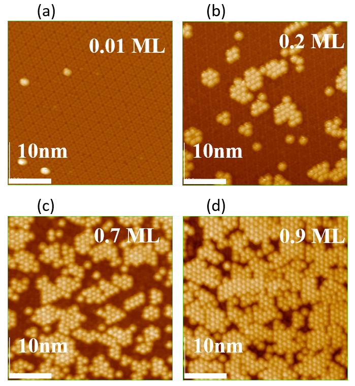 Figure 1: C84 Embedded Si substrate with different coverage. Series of STM topographic images (40 x 40 nm2) showing C84 molecules adsorbed on Si(111) surface at a negative sample bias of 2 V, as measured by UHV-STM with various degrees of coverage: (a) 0.01 ML, (b) 0.2 ML, (c) 0.7 ML, and (d) 0.9 ML.
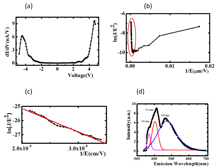 Figure 2: Electronic properties measurements on C84 Embedded Si substrate. (a) I-V curves and differential derivative conductance (dI/dV) vs the voltage curve of a single self-assembled layer of C84, as determined by UHV-STM; (b) Field emission current density vs electric field curve; (c) Corresponding F-N plot of surface with embedded C84, as measured using a source-measure unit; (d) Photoluminescence spectrum of single self-assembled layer of C84. Re-print with permission from reference12. Please click here to view a larger version of this figure.
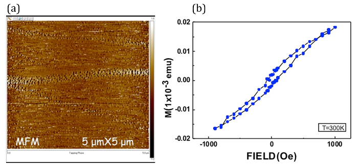 Figure 3: Surface magnetism on C84 Embedded Si substrate. (a) MFM image of Si Substrate embedded with C84; (b) Magnetization loop plotted against external magnetic field Please click here to view a larger version of this figure.
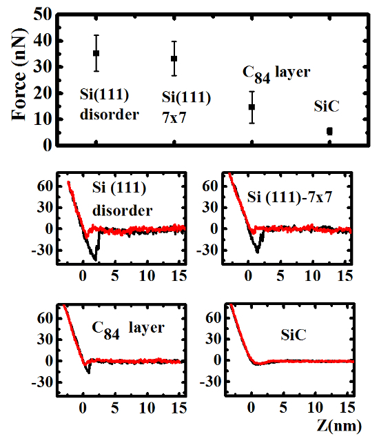 Figure 4: Nanomechanical investigation on C84 Embedded Si substrate. Force-distance analysis of disordered Si surface, 7 x 7 surface, single self-assembled layer of C84 embedded within Si surface, and Si surface, as determined using UHV-AFM. Re-print with permission from reference11. Please click here to view a larger version of this figure.
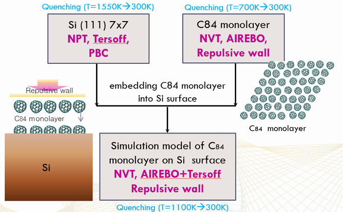 Figure 5: Flow chart for establishing simulation model. The dramatic illustrate the setting in MD simulation from a single layer C84 and Si(111) 7 x 7 surface to a C84 monolayer embed into Si(111) 7 x 7 model. The detail procedures can be seen in the section 5 of protocol. Please click here to view a larger version of this figure.
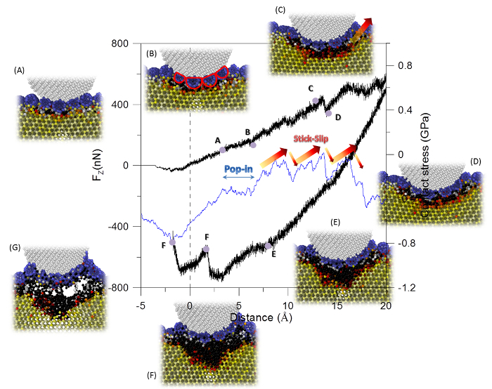 Figure 6: Indentation force and Contact stress analysis. Indentation force (black) and Contact stress (blue) of C84 as a function of indentation depth. Inserts show the corresponding snapshots, where the different color indicates the corresponding von Mises strain (εvM) of all atoms. To clear display the strain localization, only the atoms with εvM > 0.08 are shown in the snapshot. Please click here to view a larger version of this figure.
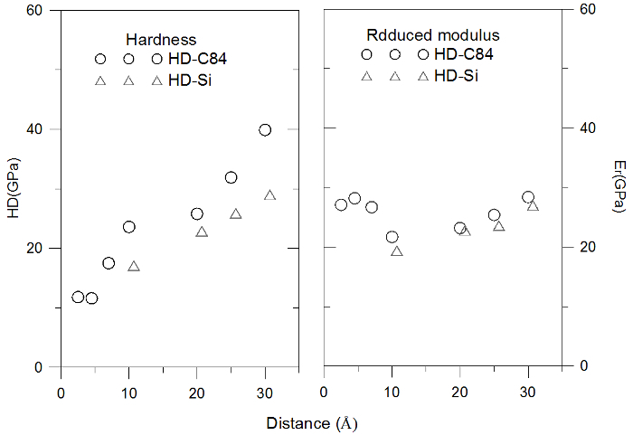 Figure 7: Hardness and reduced modulus analysis. (a) Hardness and (b) reduced modulus variation as a function of indentation depth for the C84 monolayer on Si surface. Please click here to view a larger version of this figure.
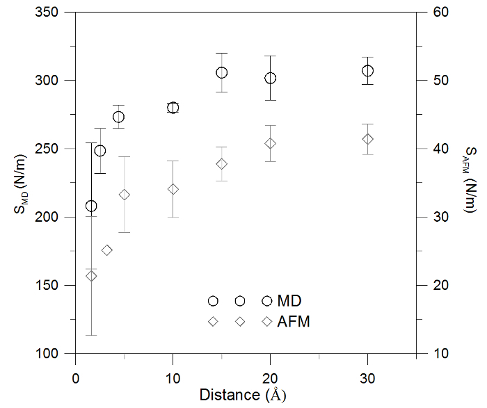 Figure 8: Loading stiffness analysis. Loading stiffness as a function of distance determined by MD simulations compared with that by AFM experiments for C84/Si. Modified from reference16. Please click here to view a larger version of this figure.
Discussion
In this study, we demonstrate the fabrication of a self-assembled monolayer of C84 on a Si substrate through a novel annealing process (Figure 1). This process can also be used to prepare other kinds of nanoparticle-embedded semiconductor substrates. The C84-embedded Si substrate was characterized at the atomic scale using UHV-STM (Figure 2), field emission spectrometer, photo-luminescence spectroscopy, MFM and SQUID (Figure 3).
The adhesion strength corresponding to nanomechanical properties (i.e., stress) of the C84-embedded Si substrates can be measured using AFM (Figure 4). Our results demonstrate that the hardness of the proposed C84-embedded Si substrate is comparable to that of SiC and Si surfaces, making it applicable as an abrasive material for cutting tools as well as a film in MEMS devices.
In the simulation section, the von Mises strain (εvM) analysis is capable to detect the local deformation of atomic structure, which is very difficult to be observed in experiment. However, it is not possible to characterize the phase transformation. Here, we suggest some useful indices such as coordination number and HA index23 to examine the phase transformation. In the setting of the indentation model, we have to point out that the size of the substrate in plan direction must be at least three times larger than diameter of the probe for eliminating the size effect and the boundary condition limitation, which would affect the dynamics and force flow of atoms.
In addition, due to the time limit of MD simulation, to study the indentation process, the probe should exert the specimen with a very fast speed compared to that in experiment. We note that such a loading speed is too high to come out the long-time atomic diffusion and migration behavior, but it is still suitable to observe and describe the plastic deformation behavior and material properties under mechanical loading24 because the results can be recognized as approximately quasi-static in nature25. An alternative theory, named Parallel Replica dynamics (PRD)26, has been developed to substantially accelerate the simulation time, but it requires heavy computing resources.
The data obtained from the MD simulation study is in agreement with the AFM indentation experiment (Figure 8); additionally, the hardness and reduced modulus of the C84-embedded Si substrate are comparable to other Si substrates. These data suggest that C84-embedded Si substrates can have significant impacts in optoelectronic and dilute magnetic semiconductor (DMS) nanodevices.
Disclosures
The authors have nothing to disclose.
Acknowledgments
The authors would like to thank the Ministry of Science and Technology of Taiwan, for their financial support of this research under Contract Nos. MOST-102-2923-E-492- 001-MY3 (W. J. Lee) and NSC-102- 2112-M-005-003-MY3 (M. S. Ho). Support from the High-performance Computing of Taiwan in providing huge computing resources to facilitate this research is also gratefully acknowledged.
References
- Kroto HW, Heath JR, O'Brien SC, Curl RF, Smalley RE. C60: Buckminsterfullerene. Nature. 1985;318:162–163. [Google Scholar]
- Zhu ZP, Gu YD. Structure of carbon caps and formation of fullerenes. Carbon. 1996;34:173–178. [Google Scholar]
- Margadonna S, et al. Crystal Structure of the Higher Fullerene C84. Chem. Mater. 1998;10:1742–1744. [Google Scholar]
- Diederich F, et al. The Higher Fullerenes: Isolation and Characterization of C76, C84, C90, C94, and C70O, an Oxide of D5h-C70. Science. 1991;252:548–551. doi: 10.1126/science.252.5005.548. [DOI] [PubMed] [Google Scholar]
- Lv Z, Deng Z, Xu D, Li X, Jia Y. Efficient organic light-emitting diodes with C60 buffer layer. Displays. 2009;30:23–26. [Google Scholar]
- Tokunaga K. On the difference in electronic properties between fullerene C60 and C60X2. Chem. Phys. Lett. 2009;476:253–257. [Google Scholar]
- Basa DK, Smith FW. Annealing and crystallization processes in a hydrogenated amorphous Si---C alloy film. Thin Solid Films. 1990;192:121–133. [Google Scholar]
- Neudeck PG, Powell JA. Performance limiting micropipe defects in silicon carbide wafers. IEEE Electron Device Lett. 1994;15:63–65. [Google Scholar]
- Huang CP, Su CC, Ho MS. Intramolecular Structures of C60 and C84 Molecules on Si(111)-7x7 Surfaces by Scanning Tunneling Microscopy. Appl. Surf. Sci. 2008;254:7712–7717. [Google Scholar]
- Huang CP, Su CC, Su WS, Hsu CF, Ho MS. Nano-measurements of electronic and mechanical properties of fullerene embedded Si(111) surfaces. Appl. Phys. Lett. 2010;97:061908. [Google Scholar]
- Huang CP, Hsu CF, Ho MS. Investigation of Fullerene Embedded Silicon Surfaces with Scanning Probe Microscopy. J. Nanosci. Nanotechnol. 2010;10:7145–7148. doi: 10.1166/jnn.2010.2877. [DOI] [PubMed] [Google Scholar]
- Huang CP, Su WS, Su CC, Ho MS. Characteristics of Si(111) surface with embedded C84 molecules. RSC Adv. 2013;3(111):9234–9239. [Google Scholar]
- Ho MS, Huang CP, inventors. Method of forming self-assembled and uniform fullerene array on surface of substrate. US9109278. US Patent. 2015
- Plimpton SJ. Fast Parallel Algorithms for Short-Range Molecular Dynamics. J. Comp. Phys. 1995;117:1–19. [Google Scholar]
- Su WS, et al. Using a functional C84 monolayer to improve the mechanical properties and alter substrate deformation. RSC Adv. 2015;5:47498–47505. [Google Scholar]
- Stukowski A. Visualization and analysis of atomistic simulation data with OVITO- the Open Visualization Tool. Modelling Simul. Mater. Sci. Eng. 2010;18:015012. [Google Scholar]
- Watson PR, Hove MAV, Hermann K. Open Surface Structure Database. 2014. Available from: http://www.fhi-berlin.mpg.de/KHsoftware/oSSD.
- Tersoff J. New empirical model for the structural properties of silicon. Phys. Rev. Lett. 1986;56:632. doi: 10.1103/PhysRevLett.56.632. [DOI] [PubMed] [Google Scholar]
- Stuart SJ, Tutein AB, Harrison JA. A reactive potential for hydrocarbons with intermolecular interactions. Journal of Chemical Physics. 2000;112:6472. [Google Scholar]
- Rapaport DC. The Art of Molecular Dynamics Simulations. Cambridge University Press; 1997. [Google Scholar]
- Fowler PW. Cn Fullerenes. 2013. Available from: http://www.nanotube.msu.edu.
- Chandra N, Namilae S, Shet C. Local elastic properties of carbon nanotubes in the presence of Stone-Wales defects. Phys. Rev. B. 2004;69:094101. [Google Scholar]
- Honeycutt JD, Andersen HC. Molecular Dynamics Study of Melting and Freezing of Small Lennard-Jones Clusters. J. Phys. Chem. 1987;91:4950. [Google Scholar]
- Schulz MJ, Kelkar AD, Sundaresan MJ. Nanoengineering of Structural, Functional and Smart Materials. Taylor & Francis; 2005. p. 736. [Google Scholar]
- Ju SP, Wang CT, Chien CH, Huang JC, Jian SR. The Nanoindentation Responses of Nickel Surfaces with Different Crystal Orientations. Molecular Simulation. 2007;33:905–917. [Google Scholar]
- Mishin Y, Suzuki A, Uberuaga BP, Voter AF. Stick-slip behavior of grain boundaries studied by accelerated molecular dynamics. Phys. Rev. B. 2007;75 [Google Scholar]


