Abstract
The significant inversion symmetry breaking specific to wurtzite semiconductors, and the associated spontaneous electrical polarization, lead to outstanding features such as high density of carriers at the GaN/(Al,Ga)N interface—exploited in high-power/high-frequency electronics—and piezoelectric capabilities serving for nanodrives, sensors and energy harvesting devices. Here we show that the multifunctionality of nitride semiconductors encompasses also a magnetoelectric effect allowing to control the magnetization by an electric field. We first demonstrate that doping of GaN by Mn results in a semi-insulating material apt to sustain electric fields as high as 5 MV cm−1. Having such a material we find experimentally that the inverse piezoelectric effect controls the magnitude of the single-ion magnetic anisotropy specific to Mn3+ ions in GaN. The corresponding changes in the magnetization can be quantitatively described by a theory developed here.
 The wurtzite crystal structure of nitride semiconductors results in strong piezoelectricity. Here, the authors also achieve electric-field control of the magnetization of gallium manganese nitride, thus showing that piezoelectric and magnetoelectric effects can be combined in the same material.
It has been known for a long time that piezoelectricity specific to crystals with no inversion symmetry offers a spectrum of outstanding functional properties. For instance, various nanoelectromechanical and energy harvesting devices employing wurtzite II–VI and III–V semiconductor compounds have recently been demonstrated1. At the same time, nanocomposite2,3 or hybrid4,5 piezoelectric/magnetic systems allow for the electric control of magnetization.
In Ga1−xMnxN system a single-ion magnetic anisotropy dominates for Mn3+ ions that assume in GaN a high-spin configuration with spin and orbital momentum S=2 and L=2, respectively6,7. For the experimental values of the lattice parameters a and c the easy axis is perpendicular to the polar [0001] direction (c axis) of the wurtzite structure6,7. At the same time a mid-gap Mn2+/Mn3+ level traps electrons introduced by Si or residual donors, so that the material becomes semi-insulating for x≳0.05% (refs 8, 9). Because of Anderson-Mott and Hubbard-Mott localization of carriers residing in the Mn impurity band, the semi-insulating character of Ga1−xMnxN persists up to the highest available Mn concentrations. In this dilute magnetic insulator, the exchange coupling between Mn3+ ions is dominated by short-range ferromagnetic superexchange interactions leading to a ferromagnetic ordering at TC≲1 K for x≲3% (ref. 10).
Here we find experimentally the existence of a strong coupling between piezoelectricity and magnetism in the dilute magnetic insulator Ga1−xMnxN and develop a theory that describes the effect quantitatively. The measurements are performed at T≥2 K and x≲3%, that is in the paramagnetic regime. Under these conditions, the inverse piezoelectric effect by stretching the elementary cell along the c axis affects the magnitude of the uniaxial magnetic anisotropy and, thus, of the magnetization. We reveal this novel magnetoelectric effect by direct magnetization measurements employing a new detection method. Our work bridges two fields of research so far independent: piezoelectricity of wurtzite semiconductors and electric control of magnetization in magnetic insulators. More specifically, the findings presented in this Communication lead to the conclusions: (i) the magnetoelectric effect generated by piezoelectricity can exist in a homogeneous crystalline compound, not only in hybrid or nanocomposite systems, (ii) the multifunctional capabilities of Ga1−xMnxN extend into the core of spintronic functionalities, like the manipulation of magnetization by the electric field.
Results
Samples
The observation of the piezoelectromagnetic effect (PEME) is built on our recent progress in the metal-organic vapour phase epitaxy (MOVPE) and nanocharacterization of wurtzite Ga1−xMnxN and Ga1−xMnxN:Si layers, which led us to fabricate a single phase homogenous alloy with Mn atoms substituting Ga sites up to x=3.5% (ref. 8). The structures studied here are grown by MOVPE onto c-plane 2″ sapphire substrates and have the c axis parallel to the growth direction and Ga-face polarity. They consist of 1 μm GaN buffer, a 500 nm-thick Si doped n+-GaN bottom contact layer (n≳1019 cm−3), and a 30 nm-thick Ga1−xMnxN or Ga1−xMnxN:Si film to which a vertical electric field can be applied. Structures with three different films have been deposited, namely: Ga1−xMnxN, Ga1−xMnxN:Si having x≃2.4 and 2.5% as established from magnetization data—denoted as A and B, respectively—and a reference structure containing Ga1−xMnxN:Si with x=0.1% (denoted as R). Samples of dimensions (5 × 5) mm2 are cut out from the wafers, and systematically characterized by atomic force microscopy (AFM), high-resolution x-ray diffraction (HRXRD), secondary-ions mass spectrometry, high-resolution transmission electron microscopy (HRTEM), and superconducting quantum interference device (SQUID) magnetization measurements.
Details on the instrumentation and on the results of the comprehensive structural and chemical characterization of the samples are collected in Methods. Both HRXRD and HRTEM images point to a high crystalline quality of the wurtzite structures, as well as reveal neither secondary phases nor relaxation defects in strained Ga1−xMnxN layers. According to the high-angle annular dark-field TEM images, Ga1−xMnxN layer thickness is t=32 nm with no indication of chemical phase separation (Mn aggregation) that might be driven by spinodal decomposition. This magnitude of t is consistent with secondary ion mass spectrometry (SIMS) data that corroborate also the values of Mn concentrations deduced from magnetization measurements on samples A, B and R discussed in the next subsection. The magnetization data confirm also that the Mn distribution is uncorrelated and that an overwhelming majority of Mn ions assumes the 3+ charge state specific to the Ga-substitutional case. Finally, we note that AFM topography reveals with the root mean square surface roughness up to 8 nm and lateral extensions in the μm range. This roughness may results in a certain inhomogeneity of the electric field applied to the structure.
Magnetization as a function of the magnetic field
Because of a relatively small film thickness and low Mn content, an accurate determination of magnetization M(T, H) for our Ga1−xMnxN layers by SQUID magnetometry has required an extension of the previous experimental methodology11. The modifications are outlined in the section Methods.
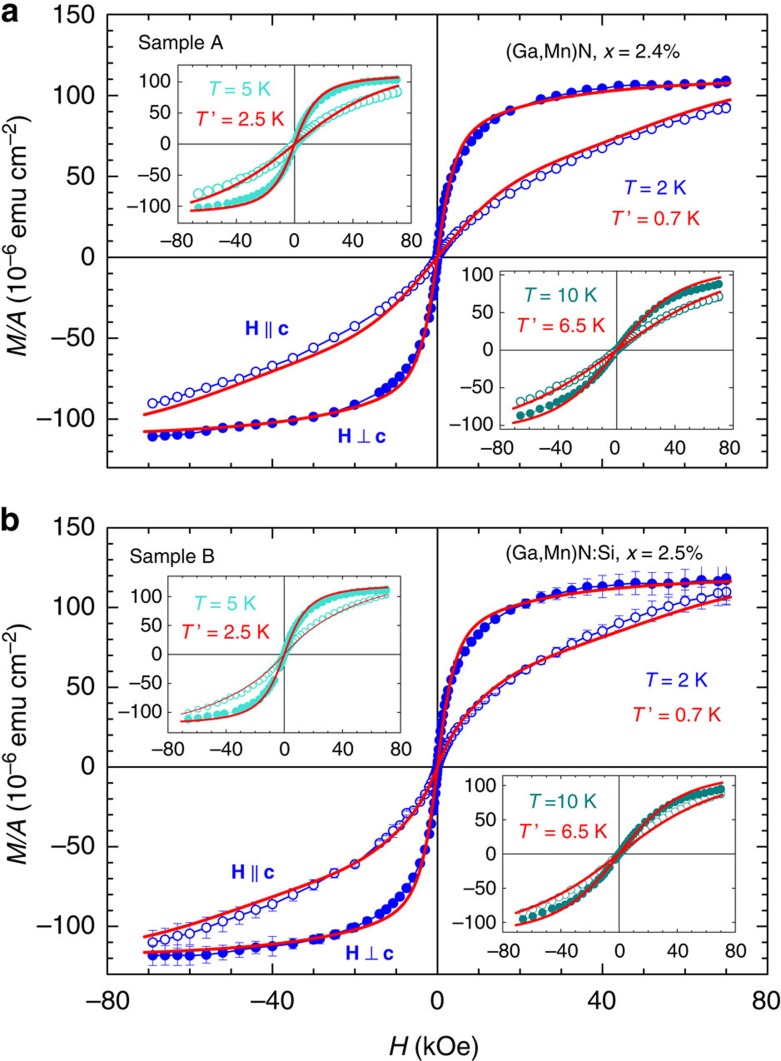
The circles in Fig. 1 represent the experimental data M(T, H) per unit sample area A for the A and B Ga1−xMnxN films at two orientations of the magnetic field H with respect to the c axis. No hysteretic behaviour is found down to the experimental noise level [σM/A(H≃0)≲1 × 10−6 emu cm−2, where A≃0.25 cm2] at any investigated temperature (2, 5, 10 K—presented in Fig. 1—and at 50 and 300 K, not shown). This points to the absence of a ferromagnetic phase that might originate from Mn-rich aggregates. This conclusion is further supported by results of HRXRD and HRTEM studies on these samples presented in Methods, and which—within the ultimate limits specific to these techniques—rule out the presence of any Mn-rich phases either in the form of nanometric precipitates or of regions of spinodal decomposition12.
Figure 1. Areal density of magnetic moment.
(a) Ga1−xMnxN (sample A) and (b) Ga1−xMnxN:Si (sample B). Results are shown for selected temperatures T as a function of the magnetic field H applied parallel (open squares) and perpendicular (closed circles) to the wurtzite c axis. For clarity, experimental error bars are provided only for measurements at 2 K for sample B. Solid lines: magnetization curves calculated for Mn3+ ions (sample A) and for Mn3+ and Mn2+ ions in the case of sample B. T′ are the values of effective temperatures adjusted to account for ferromagnetic Mn3+−Mn3+ interactions.
Actually, both layers exhibit magnetism characterized by M(T, 0)=0, M(T, H→∞) tends to saturate, and χ(T)=dM(T, H→0)/dH increases with lowering temperature according to χ(T)∝1/(T−T0). This behaviour demonstrates that the studied samples at T≥2 K are in the paramagnetic phase, though ferromagnetic coupling between neighbouring Mn spins starts to be visible and leads to T0>0. At the same time, a sizable uniaxial magnetic anisotropy is observed, M(T, H ⊥ c)>M(T, H || c), which is specific for Mn3+ ions in wurtzite GaN (refs 6, 7).
The starting point of the theory aiming in description of M(T, H) in the paramagnetic phase is a single-ion Hamiltonian in the form implied by the group theory for Mn3+ ions in wurtzite GaN (refs 6, 7). This Hamiltonian and the corresponding crystal-field, spin-orbit and Jahn-Teller parameters employed to generate theoretical curves in Fig. 1 are presented in Methods. The theoretical procedure, developed earlier for purely paramagnetic Ga1−xMnxN (x<0.6%) containing Mn3+ ions7, is modified here to describe samples with higher Mn concentrations. In particular, we introduce an effective temperature T′=T−T0(T) as a fitting parameter, where T0(T)>0 takes phenomenologically into account the presence of spin-spin coupling in dilute ferromagnets above TC. While another fitting parameter x controls the magnitude of saturation magnetization, the Crurie-Weiss-like temperature T0(T) determines, at given x, the magnitude of the slope dM(T, H→0))/dH.
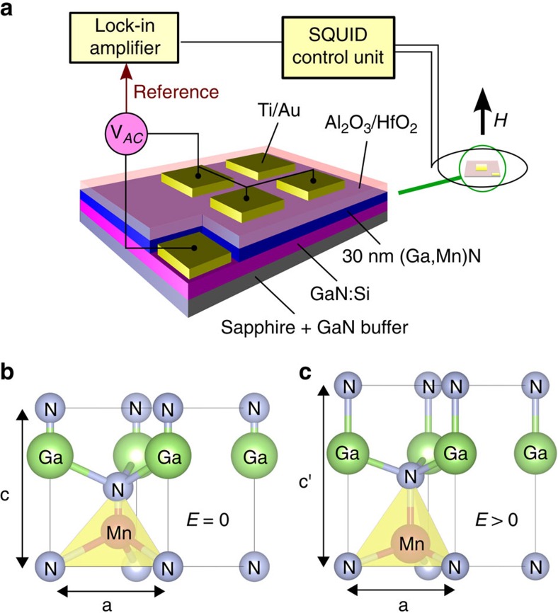
Especially relevant for our work is the quantitative interpretation of magnetic anisotropy. The single-ion magnetic anisotropy is virtually negligible for Mn2+ ions, as the orbital momentum vanishes in this case (S=5/2, L=0). In contrast, for Mn3+ ions in GaN (S=2, L=2) a sizable single-ion uniaxial magnetic anisotropy has been reported6,7. In GaN:Mn, the uniaxial anisotropy originates primarily from the trigonal deformation of the tetrahedron formed by anion atoms next to Mn, as illustrated in the panels b and c of Fig. 2. In terms of the lattice parameters a and c, the deformation is described by the parameter ξ=c/a− . In particular, for ξ<0, the case of GaN:Mn3+ , the easy axis is perpendicular to the wurtzite c axis, whereas in the opposite case ξ>0, the easy axis assumes the direction of the c axis. According to the theoretical model of Mn3+ ions (see Methods), the effect of trigonal deformation is described by two crystal field parameters,
  and
and  which, for the relevant small values ξ, can be assumed to be linear in ξ,
  =yiξ. The values of yi are known from previous investigations of thick (relaxed) Ga1−xMnxN films with x=0.4% (ref. 7), for which the fitting of magnetic anisotropy led to
  =4.2 meV and
  =−0.56 meV, whereas HRXRD measurements to a=3.191, c=5.1863 Å and, thus, ξ=−0.0077.
Figure 2. Experimental methodology.
(a) Schematic illustration of the layer structure and of the circuit used for the measurements. Capacitors containing gate oxide and semi-insulating wurtzite Ga1−xMnxN film as insulators are biased by a low-frequency a.c. electric field applied between the gate and the back contact. The structure is placed in the loop of a superconducting quantum interference device (SQUID) magnetometer; changes of the magnetic flux in phase with the electric field are detected by a lock-in amplifier connected to the output of SQUID electronics. (b,c) In the case of the c axis parallel to the growth direction and Ga-face polarity, the application of a positive voltage to the gate (E>0) stretches the Ga1−xMnxN films along the c axis affecting in this way the single-ion uniaxial magnetic anisotropy.
The lattice parameter a of our thin films is pinned by the GaN buffer. According to X-ray rocking curves and reciprocal space mapping (RSM) a=(3.1842±0.0003) Å in our samples, and this value is employed further on for the data analysis. In contrast, the minute thickness of our layers precludes a sufficiently precise experimental determination of the c parameter by HRXRD, so that we evaluate it from the magnitude of low-temperature magnetic anisotropy in sample A. This procedure leads to ξ=−0.0058.
The corresponding changes of the Jahn-Teller describing the distortion of tetragonal symmetry are unknown but a better fit is obtained by increasing their absolute values by 15% with respect to their magnitudes for x=0.4% (ref. 7), that is, to  meV and
  meV. The spin-orbit parameters are also adjusted in the same range, that is, λTT=5.5 meV, λTE=11.5 meV.
According to data in Fig. 1a,b magnetic anisotropy is weaker in Sample B. As established previously8, the doping with shallow Si donors reduces the oxidation state of a fraction z of the Mn ions from the 3+ to the 2+ charge state, as the Mn2+/3+ state resides in the mid gap region. As recalled in the theoretical part of Methods, the magnetization for Mn2+ ions in GaN is described by the isotropic Brillouin function for S=5/2. The magnitudes of x, z, and T′ are determined by fitting the combined theoretical magnetization for Mn3+ ions and Mn2+ ions with weights 1−z and z, respectively, to the whole-set of experimental data.
The most appropriate account of the experimental finding is obtained by taking x=2.4% and z=0 for sample A, whereas x=2.5% and z=0.1 for sample B. The magnitudes of the effective temperatures T′ obtained from the fitting are displayed in Fig. 1. As indicated in Fig. 1 by solid lines, the employed approach with the quoted values of the input parameters provides a correct reproduction of the experimental data.
Structure processing and experimental set-up
Having parameterized M(T, H), we turn to the measurements of the magnetic moment as a function of the electric field. In order to minimize the risk of structure damage by an electrical short via, for example, threading dislocations, two precautions are undertaken, as sketched in Fig. 2a. First, after removing by reactive ion etching (1 × 1) mm2 square down to the GaN:Si bottom contact layer, atomic layer deposition is employed to fabricate a 100 nm gate oxide (Al2O3/HfO2), which after appropriate masking is covered by Ti/Au to serve as a top capacitor plate. Second, a lift-off is used to define over a dozen of independent capacitors with an area smaller than (1 × 1) mm2. The capacitance as well as the dielectric strength and losses are measured for each of these capacitors, and only those showing no leaks are connected in parallel and studied at low temperatures. The magnitude of the resulting capacitance is equal, within the experimental accuracy, to the value expected for oxide and Ga1−xMnxN capacitors in series. This allows us to evaluate the magnitude of the electric field E applied vertically to the Ga1−xMnxN layer at a given value of the gate voltage VG. We find that this arrangement allows us to apply to Ga1−xMnxN an electric field E up to at least 5 MV cm−1, proving that doping of GaN with Mn results in a device-quality semi-insulating material. For these evaluations we employ the value of the oxide dielectric constant  =13, as determined by capacitance measurements on reference oxide capacitors. We take the dielectric constant of Ga1−xMnxN layer to be equal to the one of GaN,
  =10 (ref. 13).
In order to detect directly the effects of an electric field on magnetism we place the structured sample in the loop of a SQUID magnetometer equipped with a home-built head allowing for the electrical connections to be feedthrough down to the sample chamber. By redirecting the output of the SQUID electronics to the input of a digital lock-in nanovoltmeter, we look for the magnetic signal ME in phase with the a.c. electric field E of low frequency f, as shown in Fig. 2a. Alternatively, the film is biased by a d.c. electric field up to E=2.8 MV cm−1 and the phase sensitive detection of the slope of the ME(E) is measured with an a.c. component Emod=0.26 MV cm−1.
A noise-limited resolution of 3 × 10⁻¹¹ emu at f=1 Hz and for 2 h of lock-in output averaging has been achieved in the absence of magnetic field. Both the signal and noise increase with the magnetic field, but acquisition times up to 2 h ensure an adequate signal to noise ratio under our experimental conditions. No dependence of ME on f is found between 0.1 and 200 Hz, however f is kept below 3 Hz. The whole set-up is calibrated against a copper coil of known dimensions feeded with an a.c. current. Experiments with the coil demonstrate also the linearity of the output with the magnetic moment over the relevant range of magnetic moments independently of an external magnetic field H up to at least 20 kOe.
Magnetization as a function of the electric field
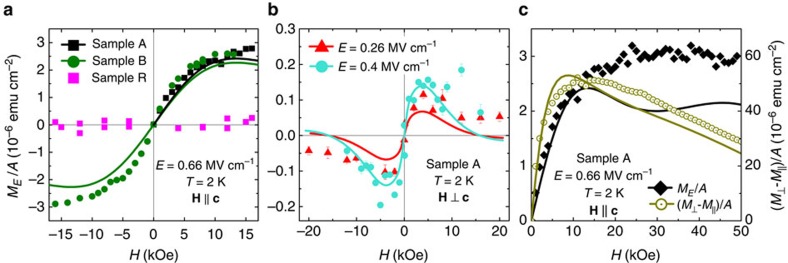
Having calibrated the system, we turn to the experimental determination of the effects of an applied electric field on magnetization. The results obtained at 2 K are summarized in Fig. 3. As indicated, no magnetic signal generated by the electric field is detected in the absence of magnetic field. This is expected as the time reversal symmetry is maintained in the paramagnetic phase and α=0 in the lowest order magnetoelectric term ME=αE (ref. 14). However, for H≠0 a sizable electric-field-induced magnetic signal ME is seen for samples A (all panels in Fig. 3) and sample B (panel a). Importantly, this signal is substantially smaller for the easy axis configuration H ⊥ c, as exemplified in Fig. 3b for sample A. Finally, we note that the magnitude of ME is below the detection limit in the case of sample R (Fig. 3a), which contains more than twenty times less Mn ions than samples A and B.
Figure 3. Magnetization changes generated by an electric field as a function of magnetic field.
Symbols: experimental data, solid lines: theory. (a) Hard axis H || c, areal density of the magnetic moment amplitude ME/A induced by electric field of the amplitude E=0.66 MV cm−1 for all studied samples. (b) Easy axis H ⊥ c, response to E=0.26 and 0.4 MV cm−1 (sample A). (c) Response to E=0.66 MV cm−1 for the hard axis H || c and difference in magnetization for the hard and easy axis (M⊥−M||)/A in a wide magnetic field range (sample A).
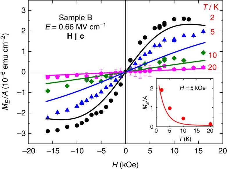
The magnitude of ME decays rapidly with increasing temperature, as exemplified in Fig. 4 for sample B. This is an expected behaviour because, according to the comparison presented in Fig. 3c, the PEME signal is directly related to the easy and hard axis magnetization difference of the material, M⊥−M||, which, on the other hand, has already been shown to vanish at T≃20 K ( Fig. 10 in ref. 7). Additionally, the samples' magnetization response to the electric field gets sizably enhanced at very low temperatures (that is on approaching TC≲1 K in our samples10). Indeed, T ′/T→0 for T→TC, as it can be inferred from Fig. 1. The whole temperature trend measured at 5 kOe is followed in the inset to Fig. 4.
Figure 4. Temperature and magnetic-field dependence of magnetization generated by the electric field.
Areal density of the magnetic moment amplitude ME/A induced by electric field of the amplitude E=0.66 MV cm−1 (sample B). Inset: temperature dependence in 5 kOe (sample B). Points and solid lines: experimental and theoretical results, respectively.
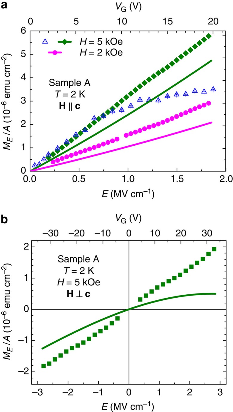
Figure 5. Magnetization as a function of the electric field.
(a) Areal density of the magnetic moment amplitude induced by electric field ME/A in the magnetic field along the hard axis is determined in two ways: (i) by applying a low-frequency sinusoidal electric field (open symbols) or (ii) by modulating the d.c. electric field by an a.c. electric field of amplitude Emod=0.26 MV cm−1 and displaying the integrated signal (closed symbols). This configuration is investigated at 2 and 5 kOe (sample A). Solid lines: theory. (b) Results for the easy axis configuration investigated at 5 kOe by the second method. The upper scales show the gate voltage VG corresponding to the electric field E.
Figure 6. Atomic force microscopy surface imaging.
Tapping mode images for all three studied layers.
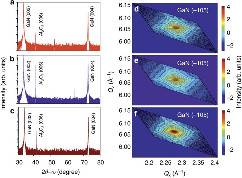
Figure 7. High-resolution X-ray diffraction data.
(a–c) Radial 2θ−ω scans of symmetric Bragg reflections for Samples A, B and R, respectively. (d–f) Reciprocal space maps of asymmetric (−105) Bragg peak for Samples A, B and R.
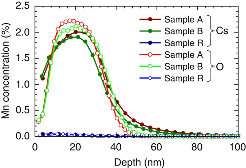
Figure 8. Secondary-ions mass spectrometry Mn-depth profiles.
The measurements are performed separately using either 133Cs+ (full symbols) or  ions (open symbols).
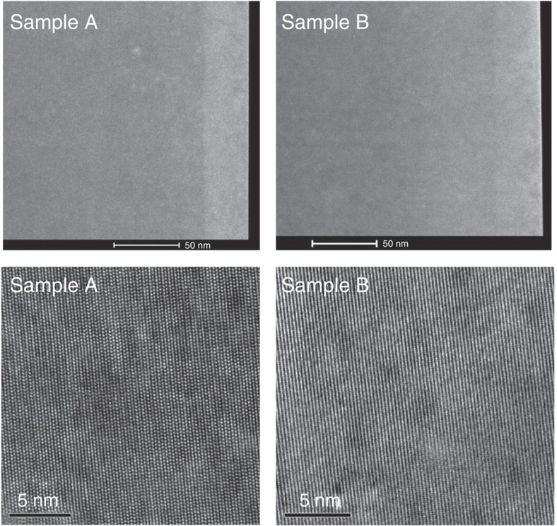
Figure 9. High-resolution transmission electron microscopy images of samples A and B.
Top row: high-angle annular dark-field/scanning transmission electron microscopy (HAADF/STEM), a contrast between GaN and 32-nm thick (Ga,Mn)N films on the top of the structures is detected with no indications of Mn aggregation. Bottom row: high-resolution transmission electron microscopy (HRTEM) images for both layers reveal their single phase nature.
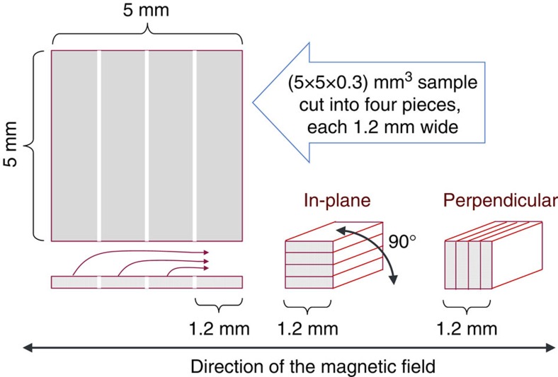
Figure 10. Experimental procedure for measuring magnetic anisotropy in thin films.
An illustration of a modification applied to a standard (here: square) sample resulting in a shape invariable with respect to 90° rotations required for setting ‘in-plane' and ‘perpendicular' experimental configurations during magnetic anisotropy studies.
According to symmetry considerations, the lowest order non-zero magnetoelectric term is ME=βHE. We test this dependency for both experimental configurations. The results obtained at 2 K are displayed in Fig. 5 and indicate that indeed a linear dependence of ME on E is experimentally observed, such a behaviour is followed both experimentally and theoretically at sufficiently low electric fields. According to Fig. 5a, the linear regime is particularly wide if the experimental values of ME are determined by integrating the a.c. magnetic response obtained in the presence of a d.c. bias of magnitude E and a weak a.c. modulation of the amplitude Emod. However, ME obtained directly as a response to the a.c. electric field modulation of amplitude E deviates from the linear dependence for E>0.8 MV cm−1. The origin of this discrepancy is unclear.
Discussion
A number of physical mechanisms has been invoked in order to explain magnetoelectric effects in various magnetic systems15,16. The proposed models include a variation of the carrier density at the interface, due to gating. Such a change alters either the strength of the exchange coupling between magnetic ions17 or the occupancy of carrier subbands with a given orientation of orbital momentum18,19,20. Another mechanism, particularly relevant for strong electric fields adjacent to a ferromagnetic metal/oxide interface is the electromigration of atoms, which affects the surface magnetic anisotropy21. In magnetic compounds showing ferroelectricity, that is, in multiferroic systems, the electric field leads to an atom rearrangement that modifies the magnetization via variations in magnetic anisotropy or spin-spin coupling2,15,16,22.
We propose here, and support our conjecture with direct quantitative computations that the changes in magnetization generated by the electric field in Ga1−xMnxN films are caused by the inverse piezoelectric effect that alters the lattice parameter c and modifies the trigonal distortion—as shown schematically in Fig. 2b,c—and, thus, modifies the uniaxial magnetic anisotropy.
According to this model, and in agreement with experimental data presented in Fig. 3, the magnitude of magnetization changes induced by the electric field depends on the orientation of the magnetic field in respect to the easy axis. A weak influence of the electric field is expected for the magnetic field along the easy axis, as in such a configuration M(H) follows approximately the Brillouin function for S=2 (see Fig. 1), meaning that it depends only weakly on the trigonal distortion ξ and, thus, on c(E). By contrast, the magnetic response for the hard configuration H || c varies strongly with ξ, as it is much reduced for ξ≠0, and tends to the Brillouin function if ξ→0, that is, when the uniaxial magnetic anisotropy vanishes.
To quantify all our E–dependent results, we adopt the value of the piezoelectric coefficient d33=2.8 pmV−1, as obtained for a clamped epitaxial GaN film23 since there is no lateral deformation in thin films deposited on thick buffer layers. Having beforehand parameterized M(T, H), as reported in Fig. 1, and knowing c(E) and, thus, ξ(E) we are in the position to determine ME(T, H) with no additional adjustable parameters. Theoretical results obtained in this way are represented by solid lines in Figs 3, 4, 5.
As seen, the model proposed here gives a good account of all experimental results as a function of the three experimentally controllable parameters: H, T and E. The level of achieved agreement indicates that the PEME dominates in the studied Ga1−xMnxN films. At the same time, it is clear that in some cases there is only qualitative agreement between experimental results and theoretical expectations (see, for example, high–field data in Fig. 3c, at 5 K in Fig. 4, and in high electric fields in Fig. 5). On the experimental side, as already noted, surface roughness detected by AFM may lead to lateral non-uniformities of the applied electric field, which can affect the behaviour of the magnetoelectric effect. It is also possible that the observed discrepancies indicate that the piezoelectric stretching not only changes the magnitude of trigonal distortion but also alters, for example, the Jahn-Teller effect or spin-spin coupling. Finally, the discrepancies may herald an onset of a contribution from a not yet identified phenomenon beyond PEME.
To put our findings in a more general perspective, it is worth recalling that dilute ferromagnetic semiconductors, such as Ga1−xMnxAs, have been playing a major role in seeding new concepts of spintronic devices and in developing our quantitative understanding of the interplay between magnetic and semiconducting properties12,24,25. Among these concepts particularly far reaching is the demonstration of magnetization control by an electric field17,19. In the present paper, this methodology has been extended to the wurtzite dilute magnetic insulator Ga1−xMnxN, in which the Fermi energy is pinned by Mn ions in the mid-gap region and the Mn3+ ions show strong single-ion anisotropy. By applying a new detection scheme, we have demonstrated magnetization control by the electric field via the inverse piezoelectric effect and developed a theory describing the PEME quantitatively. In this way, our work bridges two fields of research developed so far independently: piezoelectricity of wurtzite III–V and II–VI semiconductors1 and electrical control of magnetization in hybrid and composite magnetic structures containing piezoelectric components2,3,4,5.
According to the results presented here, the PEME shows a strong increase for T→TC. Since TC grows rapidly with x in Ga1−xMnxN (TC∝x2.2, refs 10, 26), a further progress in the incorporation of Mn into GaN will shift the magnetization control by an electric field towards higher temperatures. It is worth mentioning in this context that in addition to the influence of the inverse piezoelectric effect upon single-ion magnetic anisotropy dominating in the case considered here, an impact of the electric field upon spin–spin interactions may dominate at higher Mn concentrations. While we have detected magnetization changes by direct magnetization measurements, spin-dependent tunnelling27, spin-Hall magnetoresistance28 and magnetooptical phenomena29 may also serve to probe magnetization in magnetic insulators.
Another worthwhile outcome of the present work is the notion that the magnitude of the PEME, or more pictorially the depth of the magnetic anisotropy modulation, which depends on E and on the d33 coefficient of the given material, will be the stronger the larger is the Δξ(E)=ξ(E)−ξ(0) change with respect to ξ(0). An inversion of the magnetic anisotropy of the material (from in-plane to perpendicular, or vice versa) is expected when ξ changes sign, ξ(E)ξ(0)<0. As for many materials small magnitudes of dielectric strength or d33 may preclude obtaining a sufficiently large Δξ(E), advancements in material science may allow to engineer such a strain in layers with ξ(0)≅0 and so the condition ξ(E)ξ(0)<0 could be met and the easy magnetization axis switching could be realized with accessible electric fields. For the Ga1−xMnxN films studied here a use of compressive strain generated by an AlxGa1−xN buffer would be a viable option.
Finally, we note that according to our results Mn doping is the method to turn GaN into a high-quality semi-insulating material that sustains a strong electric field. Importantly, Mn doping does not deteriorate structural properties, as shown in Methods, up to Mn concentrations x≈3% achievable by MOVPE. This is in contrast to other transition metals, such as Fe (ref. 30) and Cr (ref. 31) that tend to aggregate into transition metal-rich nanocrystals for x≳0.5% (refs 32, 33), the process destroying their carrier trapping capabilities32. Similarly, heavy doping with C acceptors results in the dislocation formation and the appearance of self-compensating defects30,34.
Methods
Atomic force microscopy
The GaN and Ga1−xMnxN layers co-doped with Si are grown in an AIXTRON 200RF horizontal tube MOVPE reactor. Information on the morphology of the sample surface is obtained from tapping-mode AFM performed with a VEECO Dimension 3100 AFM system. The (40 × 40) μm2 area scans for Samples A, B and R are reported in Fig. 6. The root mean square surface roughness for samples A and B doped with a nominal Mn concentration of 3%, is 7.9 and 6.8 nm, respectively. For sample R with Mn concentration 0.1%, the surface roughness is estimated to be 5.5 nm.
High-resolution x-ray diffraction
HRXRD measurements have been carried out in a PANAlytical X'Pert PRO materials research diffractometer equipped with a hybrid monochromator with a 1/4° divergence slit. The diffracted beam is collected by a solid state PixCel detector with a 9.1 mm antiscatter slit. Radial 2θ−ω scans between 30° to 80° are acquired along the growth direction of GaN [0001], covering the symmetric (0002) and (0004) Bragg diffraction peaks and are shown in Fig. 7a–c. The 2θ−ω scans confirm the high crystallinity of the epitaxial layers with no precipitation of secondary phases such as Mn4N or SiN. The lattice parameters are calculated from rocking curve measurements of the symmetric (002) and asymmetric (−105) Bragg peaks. Furthermore, the full-width half maxima of the symmetric (0002) and asymmetric (−1015) reflections are estimated to be 150–160 arcsec.
RSM—that is, the scanning of a two-dimensional region of a crystal in the reciprocal space—provide information on interplanar spacings and on the effect of structural defects on the crystal arrangement. The intensity in a RSM is the projection of the three-dimensional intensity of the diffraction reflexes on a two-dimensional plane. In the RSMs reported in Fig. 7d–f, for the measured samples A, B and R, the broadening in the Qx direction is assigned to sample tilt, finite lateral coherence length of mosaic blocks and to compositional fluctuations. The absence of broadening of the peak intensity along the Qz direction indicates that the considered Ga1−xMnxN and GaN:Si layers are strained on the GaN buffer.
Secondary-ions mass spectrometry
The SIMS measurements have been performed in a Cameca IMS 6 F using either 133Cs+ or  ions, and are presented in Fig. 8 for samples A, B and R. The profiles confirm the nominal thickness of the Mn-containing layers (30 nm) and are consistent with the Mn concentration established from the saturation moment at 2 K (2.4 and 2.5% for samples A and B, respectively, as given in the main text).
High-resolution transmission electron microscopy
HRTEM measurements have been carried out employing a FEI Titan Cubed 80–300 scanning transmission electron microscope (STEM). High-angle annular dark-field images (top row of Fig. 9) show a contrast between GaN and the top Ga1−xMnxN, whose thickness is evaluated to be 32 nm for both samples, in a good agreement with the nominal value of 30 nm. No hint of Mn aggregation is detected. HRTEM images (bottom row in Fig. 9), similarly to HRXRD, demonstrate the absence of crystalline phase separation in the studied layers.
SQUID magnetization measurements
Among the many factors limiting the credibility of magnetometry in nanomagnetism, exhaustively discussed previously11, the presence of bulky substrates with a magnetic moment typically larger than those of the measured films is the most detrimental one. At first glance, the most appropriate approach calls for a direct subtraction of the magnetic response of the clear substrate at the matching fields and temperatures and then scaled according to its mass. However, such procedure yields a proper result only when the investigated sample and a reference have commensurate shapes as, actually, the real moment of the measured specimen is m(T, H)/γ, where γ≃1 is the coupling factor of a uniformly magnetized body with finite pick-up coils of a SQUID magnetometer. For a point object γ=1. Table 1 in ref. 11 lists γ values for some of the most typical sample shapes, indicating that actually it is the substrate's highly nonsymmetrical shape that introduces the most significant error in the magnetic anisotropy data. Indeed, (γ||−γ⊥)/γ||≈5% for a typical tile shaped samples, introducing an error easily exceeding the magnitude of the investigated anisotropy, particularly in strong magnetic fields.
In order to mitigate this challenge, both the original (5 × 5 × 0.3) mm3 samples and a piece of matching sapphire substrate have been diced into four ∼1.2 mm wide strips and glued to form a cuboid of a square cross-section, (1.2 × 1.2 × 5) mm3, as illustrated in Fig. 10. In this way, both in-plane and perpendicular measurements can be carried out upon a simple rotation of the specimen by 90° along its length, thus preserving γ, and using the same sample holder, the procedure assuring the required reproducibility of the experimental conditions.
Theoretical model and relevant material parameters
In the case of Mn2+ ions for which the ground state is the orbital singlet (S=5/2, L=0) in Ga1−xMnxN the magnitude of magnetization is given by the Brillouin function BS,
 |
where g=2.0, N0=44.1 nm−3 is the cation concentration, xMn2+=0 for sample A and 0.1x for sample B, and S=5/2.
Because of a non-zero value of the orbital momentum, the description of magnetization generated by Mn3+ ions is more complex. According to the group theory the energy structure of a single Mn3+ ion in wurtzite GaN can be described by the Hamiltonian6,7,35,
 |
where  describes the crystal filed of the tetrahedral Td symmetry,
  corresponds to the trigonal distortion along the GaN hexagonal c axis, which lowers the symmetry to C3V,
  gives the static Jahn-Teller distortion of the tetragonal symmetry,
  represents the spin–orbit interaction, and
  is the Zeeman term. Here
  ,
,  represent Stevens equivalent operators for a tetragonal distortion along one of the cubic [100] axes and the trigonal axis [111]||c, respectively. In general, to take into account the fact that the hybridization of the d wave function with the ligand wave function is different for the 5T2 and 5E states, three different spin-orbit parameters: λTT, λTE, and λEE=0 are introduced6,35.
The ground state of the Mn3+ ion is an orbital and spin quintet 5D with L=2 and S=2. The term HCF splits the 5D ground state into two terms of symmetry 5E and 5T2 (ground term). The 5E−5T2 splitting is ΔCF=120B4. The nonspherical Mn3+ ion undergoes further Jahn-Teller distortion, that lowers the local symmetry and splits the ground term 5T2 into an orbital singlet 5B and an higher located orbital doublet 5E. The trigonal field splits the 5E term into two orbital singlets and slightly decreases the energy of the 5B orbital singlet. The spin-orbital term yields further splitting of the spin orbitals. Finally, an external magnetic field lifts all of the remaining degeneracies.
For the crystal under consideration, there are three Jahn-Teller directions: [100], [010] and [001] (center A,B,C, respectively)6,35.
The energy level scheme of the Mn3+ ion is calculated through a numerical diagonalization of the full 25 × 25 Hamiltonian (2) matrix. The resulting magnetization assumes then the form,
 |
where xMn3+=x for sample A and 0.9x for sample B, Zi (i=A, B or C) are the partition function of the i-th center, Z=ZA+ZB+ZC, and
 |
where Eji and  are the j-th energy level and the eigenstate of the i-th center, respectively, and T′=T−T0(T) is a fitting parameter taking into account ferromagnetic interactions between Mn3+ ions.
Although, the values of the crystal field, Jahn-Teller and spin-orbit parameters for wurtzite Ga1−xMnxN can be found in literature they are specific either to strongly compensated bulk crystals of very low Mn content but high O and Mg concentrations6,35 or to thick (unstrained) epitaxial layers of significantly smaller Mn contents7 than in our case. Therefore, as already pointed out in the main text, the parameter values are adjusted to reproduce the initial magnetization data (Fig. 1) for epitaxially strained epilayers with a relatively high Mn concentrations studied in our work. As explained in the main text, a particularly sizable modification is expected for the parameters  and
and  , as they describe the trigonal deformation, so that they are linear in ξ=c/a−
 ,
,  =yiξ. Namely, we use: B4=11.44 (11.44) meV ξ=−0.0058 (−0.0077), y2=−550 (−550) meV y4=73 (73) meV,
  (−5.1) meV,
  (−1.02) meV, λTT=5.5 (5.0) meV, λTE=11.5 (10.0) meV, and λEE=0 (0), where the numbers in parentheses correspond to the very dilute Ga1−xMnxN unstrained epilayers7.
In calculations of the PEME, the value ξ(E) is obtained from [c(E)−c(0)]/c(0)=Ed33, where d33=2.8 pmV−1 (ref. 23) and c(0) is determined from ξ(0)=−0.0058 and the clamped value of a=3.1842 Å, known from the HRXRD measurements.
Data availability
The data that support the findings of this study are available from the corresponding author upon request.
Additional information
How to cite this article: Sztenkiel, D. et al. Stretching magnetism with an electric field in a nitride semiconductor. Nat. Commun. 7, 13232 doi: 10.1038/ncomms13232 (2016).
Publisher's note: Springer Nature remains neutral with regard to jurisdictional claims in published maps and institutional affiliations.
Supplementary Material
Acknowledgments
We thank Elżbieta Łusakowska for some of AFM measurements. The work is supported by the Narodowe Centrum Nauki (Poland) through projects MAESTRO (2011/02/A/ST3/00125), OPUS (2013/09/B/ST3/04175) and FUGA (2014/12/S/ST3/00549), by the Austrian Science Foundation—FWF (P22477, P24471 and P26830), by the NATO Science for Peace Programme (Project no. 984735), and by the European Commission through the 7th Framework Programmes: CAPACITIES project REGPOT-CT-2013-316014 (EAgLE), and Horizon2020 Project NMP645776 ALMA.
Footnotes
Author contributions The work was planned and proceeded by discussions among A.B., M.S., and T.D. Samples growth by MOVPE and their structural characterization by AFM and HRXRD were carried out by R.A. and A.B. Atomic layer deposition and RIE were performed by K.K., R.K., and A.P., whereas R.J. and T.L. carried out SIMS and TEM studies, respectively. K.G. and M.S. performed SQUID magnetization measurements, whereas D.S., M.F., G.P.M. and M.S. processed the samples and made SQUID studies in the electric field with an input of M.Z. Analysis and interpretation of the data were accomplished by D.S. and T.D. The manuscript was written by D.S., M.F., G.P.M., A.B., M.S., and T.D. with inputs from all the authors.
References
- Wen X. et al. Development and progress in piezotronics. Nano Energy 14, 276–295 (2015). [Google Scholar]
- Fiebig M. Revival of the magnetoelectric effect. J. Phys. D: Appl. Phys. 38, R123–R152 (2005). [Google Scholar]
- Maceiras A. et al. High-temperature polymer based magnetoelectric nanocomposites. Europ. Polymer J. 64, 224–228 (2015). [Google Scholar]
- Botters B. et al. Stress dependence of ferromagnetic resonance and magnetic anisotropy in a thin NiMnSb film on InP(001). Appl. Phys. Lett. 89, 242505 (2006). [Google Scholar]
- D'Souza N., Fashami M. S., Bandyopadhyay S. & Atulasimha J. Experimental clocking of nanomagnets with strain for ultralow power Boolean logic. Nano Lett. 16, 1069–1075 (2016). [DOI] [PubMed] [Google Scholar]
- Gosk J. et al. Magnetic anisotropy of bulk GaN:Mn single crystals codoped with Mg acceptors. Phys. Rev. B 71, 094432 (2005). [Google Scholar]
- Stefanowicz W. et al. Structural and paramagnetic properties of dilute Ga1−xMnxN. Phys. Rev. B 81, 235210 (2010). [Google Scholar]
- Bonanni A. et al. Experimental probing of exchange interactions between localized spins in the dilute magnetic insulator (Ga,Mn)N. Phys. Rev. B 84, 035206 (2011). [Google Scholar]
- Yamamoto T. et al. Reduction in buffer leakage current with Mn-doped GaN buffer layer grown by metal organic chemical vapor deposition. Japan. J. Appl. Phys. 52, 08JN12 (2013). [Google Scholar]
- Sawicki M. et al. Origin of low-temperature magnetic ordering in Ga1−xMnxN. Phys. Rev. B 85, 205204 (2012). [Google Scholar]
- Sawicki M., Stefanowicz W. & Ney A. Sensitive SQUID magnetometry for studying nano-magnetism. Semicon. Sci. Technol. 26, 064006 (2011). [Google Scholar]
- Dietl T. et al. Spinodal nanodecomposition in semiconductors doped with transition metals. Rev. Mod. Phys. 87, 1311–1377 (2015). [Google Scholar]
- Barker A. S. Jr & Ilegems M. Infrared lattice vibrations and free-electron dispersion in GaN. Phys. Rev. B 7, 743–750 (1973). [Google Scholar]
- Dzyaloshinskii I. E. On the magneto-electrical effect in antiferromagnets. Soviet Phys. JETP 10, 628–629 (1960). [Google Scholar]
- Matsukura F., Tokura Y. & Ohno H. Control of magnetism by electric fields. Nat. Nanotechnol. 10, 209–220 (2015). [DOI] [PubMed] [Google Scholar]
- Fusil S., Garcia V., Barthelemy A. & Bibes M. Magnetoelectric devices for spintronics. Annu. Rev. Mater. Res. 44, 91–116 (2014). [Google Scholar]
- Ohno H. et al. Electric-field control of ferromagnetism. Nature 408, 944–946 (2000). [DOI] [PubMed] [Google Scholar]
- Sawicki M. et al. Temperature dependent magnetic anisotropy in (Ga,Mn)As layers. Phys. Rev. B 70, 245325 (2004). [Google Scholar]
- Chiba D. et al. Magnetization vector manipulation by electric fields. Nature 455, 515–518 (2008). [DOI] [PubMed] [Google Scholar]
- Shiota Y. et al. Induction of coherent magnetization switching in a few atomic layers of FeCo using voltage pulses. Nat. Mater. 11, 39–43 (2012). [DOI] [PubMed] [Google Scholar]
- Bauer U. et al. Magneto-ionic control of interfacial magnetism. Nat. Mater. 14, 174–181 (2014). [DOI] [PubMed] [Google Scholar]
- Spaldin N. A. & Ramesh R. Electric-field control of magnetism in complex oxide thin films. MRS Bulletin 33, 1047–1050 (2008). [Google Scholar]
- Guy I. L., Muensit S. & Goldys E. M. Extensional piezoelectric coefficients of gallium nitride and aluminum nitride. Appl. Phys. Lett. 75, 4133–4135 (1999). [Google Scholar]
- Dietl T. & Ohno H. Dilute ferromagnetic semiconductors: physics and spintronic structures. Rev. Mod. Phys. 86, 187–251 (2014). [Google Scholar]
- Jungwirth T. et al. Spin-dependent phenomena and device concepts explored in (Ga,Mn)As. Rev. Mod. Phys. 86, 855–896 (2014). [Google Scholar]
- Stefanowicz S. et al. Phase diagram and critical behavior of a random ferromagnet Ga1−xMnxN. Phys. Rev. B 88, 081201(R) (2013). [Google Scholar]
- Miao G.-X., Chang J., Assaf B. A., Heiman D. & Moodera J. S. Spin regulation in composite spin-filter barrier devices. Nat. Commun. 5, 3682 (2014). [DOI] [PubMed] [Google Scholar]
- Nakayama H. et al. Spin hall magnetoresistance induced by a nonequilibrium proximity effect. Phys. Rev. Lett. 110, 206601 (2013). [DOI] [PubMed] [Google Scholar]
- Suffczynski J. et al. Effects of s,p-d and s-p exchange interactions probed by exciton magnetospectroscopy in (Ga,Mn)N. Phys. Rev. B 83, 094421 (2011). [Google Scholar]
- Heikman S., Keller S., DenBaars S. P. & Mishra U. K. Growth of Fe doped semi-insulating GaN by metalorganic chemical vapor deposition. Appl. Phys. Lett. 32, 439–441 (2002). [Google Scholar]
- Mei F. et al. Growth and characterization of Cr-doped semi-insulating gan templates prepared by radio-frequency plasma-assisted molecular beam epitaxy. J. Cryst. Growth 353, 162–167 (2012). [Google Scholar]
- Bonanni A. et al. Paramagnetic GaN:Fe and ferromagnetic (Ga,Fe)N: The relationship between structural, electronic, and magnetic properties. Phys. Rev. B 75, 125210 (2007). [Google Scholar]
- Gu L. et al. Characterization of Al(Cr)N and Ga(Cr)N dilute magnetic semiconductors. J. Magn. Magn. Mater. 290, 1395–1397 (2005). [Google Scholar]
- He X. et al. Unintentionally doped semi-insulating GaN with a low dislocation density grown by metalorganic chemical vapor deposition. J. Vac. Sci. Technol. B 32, 051207 (2014). [Google Scholar]
- Wolos A. et al. Neutral Mn acceptor in bulk GaN in high magnetic fields. Phys. Rev. B 70, 245202 (2004). [Google Scholar]
Associated Data
This section collects any data citations, data availability statements, or supplementary materials included in this article.
Supplementary Materials
Data Availability Statement
The data that support the findings of this study are available from the corresponding author upon request.


