Abstract
Zinc oxide (ZnO) nano thin films have been deposited by the chemical double-dip technique using aqueous ZnSO4 and NaOH solutions. The ZnO films were characterized in terms of surface morphology by x-ray diffraction, energy-dispersive x-ray analysis (EDX), the use of a scanning electron microscope (SEM) and atomic force microscope (AFM) for surface morphology. The films exhibited a smooth morphology. The chemical states of oxygen and zinc in the ZnO nano thin films were also investigated by x-ray photoelectron spectroscopy (XPS). In the present investigations, highly textured ZnO thin films with a preferential (002)-orientation were prepared on glass substrates. The deposition conditions were optimized to obtain device-quality films for practical applications.
Keywords: ZnO, chemical deposition, SEM, AFM, XPS
Introduction
Zinc oxide (ZnO) is one of the most widely studied direct wide-band-gap (3.2 eV) materials of the II–VI family of semiconductors [1]. It has promising applications such as an inexpensive, anticorrosive n-type semiconductor, and as transparent conductive contacts, solar cells, gas sensors, laser diodes, ultraviolet lasers and thin-film transistors. ZnO thin films have attracted considerable attention because they can be tailored to possess high electrical conductivity, high infrared reflectance and high visible transmittance upon applying by different coating techniques. Furthermore, zinc is a cheap and abundant raw material [2–6]. Different methods such as spray pyrolysis [7] and chemical deposition [8] have been applied to obtain ZnO thin films. The chemical deposition of ZnO films from aqueous solutions is a very promising method because of its simplicity and economy. The chemical bath deposition (CBD) technique is an open-bath wet-chemical method that has been extensively employed for the synthesis of metal oxide thin films. In this paper, we report the chemical growth of ZnO thin film by the double-dip technique reported by Mitra and Kahn [8], and the characterization results of the grown films. The structure, surface morphology and microstructure parameters are investigated and reported.
Experimental
The ZnO thin films were deposited on glass substrates (microscope slides) by alternately dipping of the substrates in a sodium zincate (Na2ZnO2) bath at room temperature and hot water maintained nearly at boiling point. The same technique of successive immersions in two separate solutions has been employed for the preparation of Cu2O thin films by Ristov et al [9]. The sodium zincate bath was prepared by adding sodium hydroxide (NaOH) to an aqueous solution of zinc sulphate (ZnSO4). The concentration of ZnSO4 was varied from 0.075 to 0.125 M in steps of 0.025 M. 2 M NaOH was added to the aqueous solution of ZnSO4 for the preparation of sodium zincate. The glass substrates were cleaned before deposition using chromic acid followed by rinsing in distilled water and cleaning with acetone and alcohol. The clean substrate was first immersed in the sodium zincate bath for 10 s (first dip) and then dipped in hot water for the same duration (second dip). In this way, a thin layer of sodium zincate complexes, is formed during the first dip, which decomposes to ZnO when subsequently dipped in hot water. The equations for the formation of ZnO thin films are as follows:
Part of the thus-formed ZnO was deposited on the glass substrate as a strongly adherent film [10], and the remaining ZnO were formed as precipitate in the solution. ZnO films deposited with 100 dippings were dried in air and subsequently annealed at a temperature of 200 °C for 10 min.
The film thickness was determined by the weight gain method using the formula
where t is the thickness of the film, m is the weight gain, A is the area of the deposited film and ρ is the density of the film (5.6 g cm- 3, as reported in the literature) [11]. The film thickness was found to be approximately 1.6 μ m, which was standardized by measurements using a Dektak profilometer.
The deposition was carried out at ZnSO4 concentrations of 0.075, 0.1 and 0.125 M and pH values of 8 ± 0.2, 9 ± 0.2 and 10 ± 0.2. The deposition was optimized at a pH of 9 ± 0.2 in terms of structural properties and morphology as revealed using a scanning electron microscope (SEM) and by energy dispersive x-ray analysis (EDX), which were used to estimate the formation of crystallites and to evaluate the composition of the film, respectively. The composition was also studied by x-ray photoelectron spectroscopy (XPS) measurements.
The structural properties of the film were studied by x-ray diffraction (XRD) analysis using an X'-pert Pro PANalytical CuKα diffractometer (λ = 0.1542 nm) by varying the diffraction angle 2θ with a step width of 0.02°. Surface morphological and compositional analyses were carried out using an SEM and an EDX setup attached to the SEM (Hitachi–S 3000 H model), respectively. Atomic force microscopy (AFM) was carried out using a Veeco Digital Instruments D3100 (United States). XPS measurements were performed using a LAS-3000 surface analysis system (RIBER, France) and AlKα x-rays (1489.6 eV, width 0.5 eV).
Results and discussion
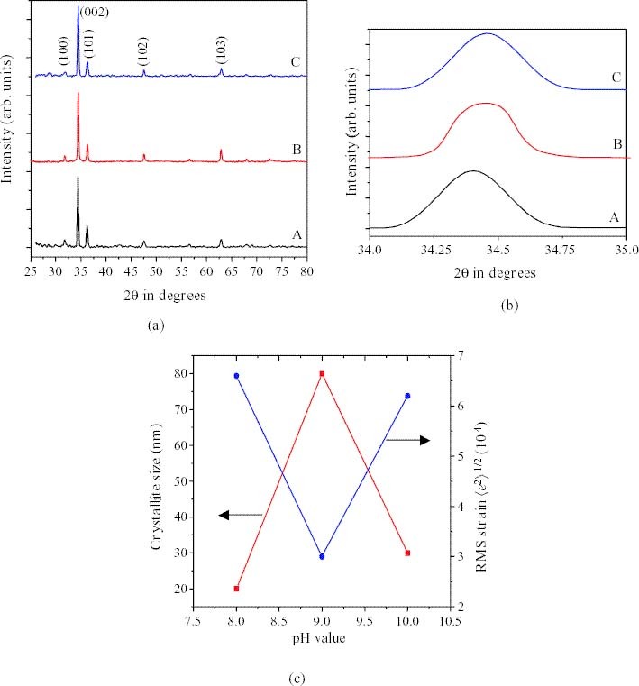
XRD patterns recorded for ZnO films on glass substrates grown by chemical double-dip deposition at various pHs are shown in figure 1. The studies revealed that the ZnO films are polycrystalline with a hexagonal wurtzite structure. The different peaks in the diffraction pattern were indexed and the corresponding value of the interplanar spacing d was calculated. The observed value of d is in good agreement with ASTM data [12]. A slow XRD scan was used to calculate the crystallite size using Scherrers' formula [13]:
where p is the crystallite size, λ is the wavelength, β is the full-width at half-maximum (FWHM) and θ is the diffraction angle, and the grain size was found to be approximately 80 nm. It was also observed from the XRD patterns that the crystallites are preferentially oriented along the (002) plane. Figure 1(b) shows the shift in the peak position of the 002 reflection, which was the most prominent peak. It was observed that the shift is towards higher angles for the films grown at pH = 9 ± 0.2 and 10. However, the peak shift is found to be very small from that at pH = 9 ± 0.2 to that at pH of 10 ± 0.2. This may be due to the increase in the bond length of the films during growth at pH = 9 ± 0.2 and the further increase of pH has little effect on the bond-length increase. Hence the bath used for the film growth was maintained at pH = 9 ± 0.2.
Figure 1.

(a) XRD patterns of zinc oxide thin films grown at a pH of (A) 8, (B) 9 and (C) 10 by the chemical double-dip method. (b) Enlarged region of the (002) plane showing the shift in the XRD peak due to effect of the pH, and (c) Variation of crystallite size and RMS microstrain for ZnO thinfilms under the effect of pH at (A) 8, (B) 9 and (C) 10.
Assuming that the broadening of the diffraction peak is due to both crystallite size and strain, the variance of 2θ values can be written as
where 2θ is the angular range over which the intensity is appreciable and 〈e2〉 is the mean squared strain. Dislocation density ‘ρ' [14] is defined as the length of the dislocation lines per unit volume of the crystal. Williamson and Smallman [15] suggested a method of calculating the dislocation density using the expression
 |
where 〈e2〉 1/2 is the RMS strain. The RMS strain is evaluated using equations (5) and (6). Figure 1(c) shows the variations of crystallite size and RMS micro strain for ZnO thin films with respect to pH. It is clear from figure 1(c) that the films grown at pH 9 ± 0.2 exhibited the least RMS strain and the greatest crystallite size.
Morphological studies
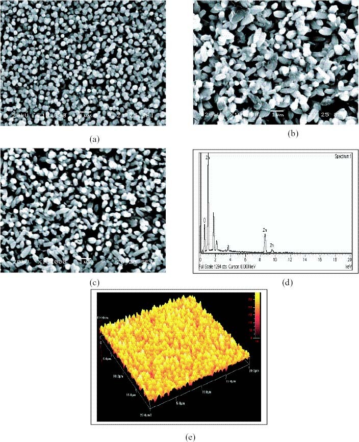
The SEM micrographs recorded at 20 kV with magnification 10 K are shown in figures 2(a)–(c). The films grown at pH = 8 ± 0.2 had spherical grains with voids distributed uniformly throughout the surface. The films were uniform and the particulates (grains) were very small. The films grown at pH = 10 ± 0.2 also had voids but the crystallite size and electrical contact between the grains were improved. The SEM micrograph of the films grown at pH 9 ± 0.2 shows large, highly crystalline grains distributed uniformly with maximum electrical contact. This shows that a pH of 9 ± 0.2 is favourable for the deposition of a uniform film surface. All micrographs show films with excellent uniformity and regularly stacked nanorods. The nanorods were found to be made of nanostructures with size between a few nanometers and 80 nm. Using AFM (figure 2(e)) it was possible to measure the surface roughness of the films over a 20 × 20 μ m2 area in contact mode, which revealed low surface roughness for the films grown at pH = 9 ± 0.2.
Figure 2.

SEM micrograph of ZnO thin films obtained by chemical double-dip method with 100 dippings. (a) pH 8 ± 0.2, (b) pH 9 ± 0.2 and (c) pH 10 ± 0.2. (d) EDX spectrum of ZnO thin film and (e) AFM micrograph of ZnO film.
Compositional analysis
The composition of the optimized film was estimated by EDX. Figure 2(d) shows the EDX result, which revealed a composition of O/Zn = 67.54/32.46 atm%. The films deposited at water bath temperatures above 90 °C (for the second dip) have an excess O content. This result is consistent with the XRD analysis of the film. According to our analysis, the films were optimally deposited at a temperature of 95 °C, a pH of 9 ± 0.2 and using 0.1 M ZnSO4, which resulted in nearly stoichiometric films.
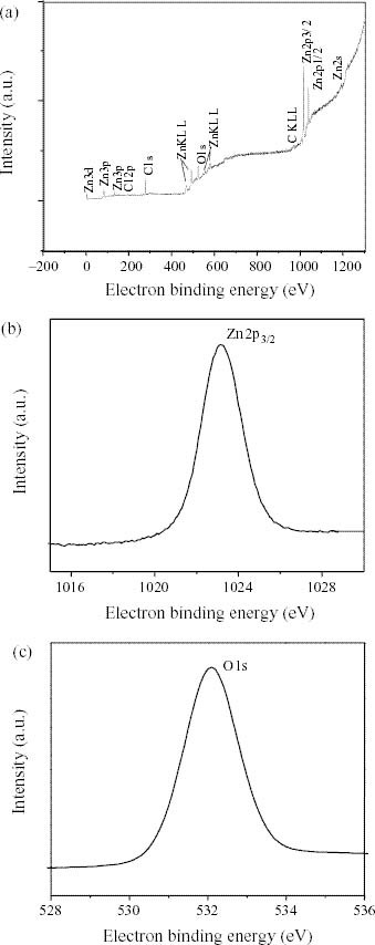
XPS measurements were performed to investigate the chemical states of Zn and O in the n-type ZnO films. Figure 3(a) shows the complete XPS spectrum of a ZnO film grown at room temperature. The elements Zn, O and C were found in the spectrum. The core levels of Zn and O can be seen in figures 3(b) and (c), respectively, in which the Zn(2p3/2) peak is centered at 1023.1 eV and the O (1s) peak is centered at 532.1 eV, in good agreement with the literature [9]. The highly electropositive Zn2 + with two donated electrons is in a highly electronegative environment with charged O2 - ions in the geometry of a Wurtzite structure. This essentially agrees with the chemical states of Zn and O atoms obtained from the XPS spectrum. The composition estimated by XPS using the relative sensitivity factors of Zn and O also revealed excess oxygen in the films. The EDX and XPS results are in good agreement.
Figure 3.

(a) Complete XPS spectrum of ZnO nano thin film, (b) XPS spectrum of Zn(2p3/2) and (c) XPS spectrum of O (1s).
Conclusion
The feasibility of ZnO thin film nanostructure preparation in an aqueous medium by a simple chemical double-dip technique was demonstrated. An XRD study showed that ZnO films deposited using 0.1 M ZnSO4 solution in the first dip followed by a dip in a hot water bath at a temperature of 95 °C are polycrystalline with strong preferential orientation along the (002)-plane. The microstructural parameters were estimated and were found to depend on the temperature of the hot water bath, the pH and the ZnSO4 concentration. The growth of ZnO films with excellent crystallinity and surface uniformity was achieved at the optimized conditions of 100 dippings in a bath with a molar concentration of 0.1 M and a pH of 9 ± 0.2. SEM and AFM analyses confirmed the uniformity of the films, which was comparable to that of films grown by cost-intensive physical methods. The Zn(2p3/2) and O (1s) XPS peaks observed in the as-deposited film were highly symmetric.
Acknowledgments
TAV and RC are grateful to the University Grants Commission (UGC), Hyderabad, India for the financial support given to carry out this work.
References
- Wang Z L. Mater. Today. 2004;7:26. doi: 10.1016/S1369-7021(04)00286-X. [DOI] [Google Scholar]
- Ozgu I U, Alivov Ya I, Liu C, Take A, Reshchikov M A, Dogan S, Avrutin V, Cho S J. and Morkoc H. J. Appl. Phys. 2005;98:041301. doi: 10.1063/1.1992666. [DOI] [Google Scholar]
- Wang Z L. J. Phys.: Condens. Matter. 2004;16:R829. doi: 10.1088/0953-8984/16/25/R01. [DOI] [Google Scholar]
- Bahadur H, et al J. Mater. Sci. 2006;41:7562. doi: 10.1007/s10853-006-0841-x. [DOI] [Google Scholar]
- Bahadur H, Srivastava A K, Sharma R K. and Chandra S. Nanoscale Res. Lett. 2007;2:469. doi: 10.1007/s11671-007-9089-x. [DOI] [Google Scholar]
- Suzuki S, Miyata T, Ishii M. and Minami T. Thin Solid films. 2003;434:14. doi: 10.1016/S0040-6090(03)00463-2. [DOI] [Google Scholar]
- Hsiao K C, Liao S C. and Chen Y J. Mat. Sci. Eng. 2007;A 447:71. doi: 10.1016/j.msea.2006.10.116. [DOI] [Google Scholar]
- Mitra P. and Khan J. Mater. Chem. Phys. 2006;98:279. doi: 10.1016/j.matchemphys.2005.09.042. [DOI] [Google Scholar]
- Ristov M, Sinadinovski G J. and Grozondv O. Thin Solid Films. 1985;123:63. doi: 10.1016/0040-6090(85)90041-0. [DOI] [Google Scholar]
- Ramamoorthy K, Arivanandhan M, Sankaranarayanan K. and Sanjeeviraja C. Mater. Chem. Phys. 2004;85:257. doi: 10.1016/j.matchemphys.2003.09.018. [DOI] [Google Scholar]
- Mitra P, Chatterjee A P. and Maiti H. J. Mater. Sci. 1998;9:441. [Google Scholar]
- ASTM data file 5.64 and 8.549 [Google Scholar]
- Cullity B D. Reading, MA: Addison-Wesley; 1956. Elements of X-ray Diffraction; p. p 99. [Google Scholar]
- Warren B E. and Warekois E P. Acta. Metall. 1955;3:473. doi: 10.1016/0001-6160(55)90138-3. [DOI] [Google Scholar]
- Williamson G K. and Smallman R E. Phil. Mag. 1956;1:34. doi: 10.1080/14786435608238074. [DOI] [Google Scholar]


