Abstract
The present status of Cs-corrected TEM/STEM is described from the viewpoint of the observation of nanomaterials. Characteristic features in TEM and STEM are explained using the experimental data obtained by our group and other research groups. Cs correction up to the 3rd-order aberration of an objective lens has already been established and research interest is focused on correcting the 5th-order spherical aberration and the chromatic aberration in combination with the development of a monochromator below an electron gun for smaller point-to-point resolution in optics. Another fundamental area of interest is the limitation of TEM and STEM resolution from the viewpoint of the scattering of electrons in crystals. The minimum size of the exit-wave function below samples undergoing TEM imaging is determined from the calculation of scattering around related atomic columns in the crystals. STEM does not have this limitation because the resolution is, in principle, determined by the probe size. One of the future prospects of Cs-corrected TEM/STEM is the possibility of extending the space around the sample holder by correcting the chromatic and spherical aberrations. This wider space will contribute to the ease of performing in situ experiments and various combinations of TEM and other analysis methods. High-resolution, in situ dynamic and 3D observations/analysis are the most important keywords in the next decade of high-resolution electron microscopy.
Keywords: spherical aberration correction, TEM/STEM, nanomaterials, electron diffraction, three-dimensional observation
Introduction
Atomic structure analysis is a starting point for various types of materials research. The basic atomic structure such as the unit-cell structure of crystals can be obtained by x-ray diffraction analysis; the structures of polycrystals have even recently been revealed by a powder diffraction technique and Rietveld analysis [1, 2]. The information obtained by the x-ray method is, however, information in which the variation of local structures has been smoothed out. When the samples are perfect crystals, the data obtained by the diffraction method is true data, but samples including various types of defects and fluctuations in the structure must be studied by real-space analysis methods.
Transmission electron microscopy (TEM) is a useful real-space analysis method. Because of the imperfect lens used, however, the point-to-point resolution has been limited to 0.2 nm for TEM at an accelerating voltage of 200 kV for a long time [3]. To analyze the interfaces and surface structures of semiconductors, their atomic-level observation is unsatisfactory. Since the development of spherical aberration correctors by Haider et al [4] and Krivanek et al [5], the resolution of TEM and scanning transmission electron microscopy (STEM) has been greatly improved to less than 0.1 nm. The dumbbell structures of most semiconductors can be successfully and easily resolved using new TEM/STEM instruments, and we have been able to advance to a new era of structure research in real-space.
In the present review, first we consider the various advantages of TEM and STEM equipped with spherical aberration correctors on the basis of experimental data obtained by our group and others, and then we discuss problems related to the present use and future prospects of TEM and STEM.
Advantages of Cs-corrected TEM
Improvement of point-to-point resolution
The point-to-point resolution of TEM images of a sample is expressed in terms of the phase-contrast transfer function (PCTF) when the sample is assumed to be a weak-phase object [3]. In ordinary cases of measuring the resolution, one can use thin amorphous carbon or germanium films as the samples and obtain high-resolution granular images. Digital Fourier transform (DFT) patterns give us the Scherzer limit corresponding to the point-to-point resolution and the information limits determined by the convergence of incident electrons and the chromatic aberration of the instrument. To estimate the resolutions of the latter, the Young fringe method is adopted, which uses a Fourier transform patterns from two overlapping granular images that are slightly laterally shifted during the recording using the image shift knobs of the TEM. Spherical aberration correctors have improved the Scherzer resolution, which is determined by coherent imaging with the aberration.
Figure 1 shows a simple comparison of the PCTF for a spherical aberration corrected (Cs-corrected) TEM with Cs=−30 μm and Δf=10 nm (overfocused) (a) and a conventional TEM with Cs=0.5 mm and Δf=−42.5 nm (underfocused) (b). The Scherzer resolution of the latter is about 0.2 nm, but that of the Cs-corrected TEM is 0.1 nm or less. The dumbbell structures of silicon (Si) crystals observed along the [110] direction are easily resolved using the former instrument. Figure 2 shows a typical high-resolution image of the dumbbell structure, where small black dots correspond to Si atomic columns and the white circular contrast represents vacuum tunnels [6]. Figure 3 shows a similar dumbbell image of a [110] oriented diamond crystal, which has a point-to-point resolution of 89 pm, even using the Cs-corrected TEM without a monochromator or a chromatic aberration (Cc) corrector [7].
Figure 1.
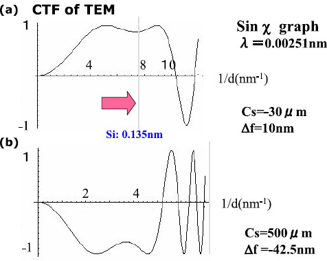
Phase contrast transfer function for Cs-corrected (a) and ordinary (b) TEMs.
Figure 2.
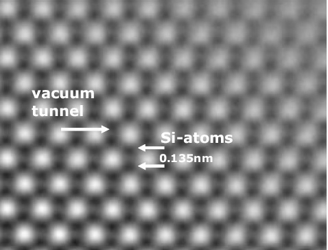
200 kV Cs-corrected TEM image of a silicon crystal observed along the [011] direction, Cs = 0 ± 1 μ m, slightly underfocused [6].
Figure 3.
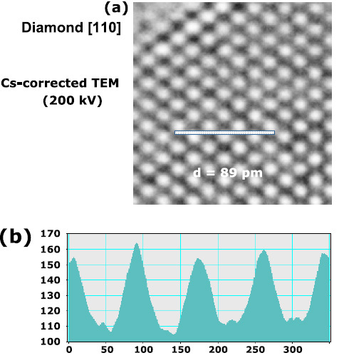
(a) 200 kV Cs-corrected TEM image of a diamond crystal along the [011] direction and (b) intensity profile along the line shown in (a). The image has a point-to-point resolution of 89 pm [7].
The point-to-point resolution of electron microscope coherent imaging is expressed by the Scherzer formula as
where Cs is the 3rd-order spherical aberration coefficient and λ the wavelength of the incident electrons [3, 8].
The resolution determined by the chromatic damping originating from the energy spread of the incident electrons, the energy loss in the sample and the chromatic aberration of the objective lens is written as
 |
where ΔE is the fluctuation of the accelerating voltage, ΔE0 is the energy loss in the sample and ΔI is the fluctuation of the lens current [3]. The value α is a half-angle used in the objective lens.
Sharp interface images without Fresnel fringes
The principle of the high-resolution electron microscopy of atomic objects was established by Scherzer in 1949 [8]. He used positively spherical aberration and defocus (1st order aberration) of an objective lens to obtain image contrast from almost pure-phase objects such as single atoms. A phase object that causes only phase modulation does not give an image contrast against background intensity in the in-focus condition (Gaussian focus). He suggested the use of the aberration of an objective lens to cancel the genuine phase shift due to scattering of π/2 in a sample and to make the sample an amplitude object, which was the same idea as that developed by Zernike in optical microscopes. For this purpose, he derived the optimum defocus condition presently called as the Scherzer defocus.
Similar treatment by defocusing to obtain image contrast is also used in the imaging of lattice fringes. In that case, we need to consider both defocusing corresponding to the period of Cowley and Moodie's Fourier images [9] and canceling the phase shift due to scattering.
The defocusing carried out to obtain such image contrast necessarily blurs images surrounded with a black or white contrast, which is particularly easily observable at interfaces and surfaces and is also referred to as Fresnel fringes. The Fresnel fringe contrast is mixed with the image contrast of lattice fringes, and this mixing results in minor shifts of the position of the lattice fringes. These shifts are problematic for the accurate determination of the positions of atomic columns at interfaces and surfaces. In Cs-corrected TEM, the Scherzer defocus approaches zero according to formula (3), and does not produce any Fresnel fringes. When one obtains high-resolution images of the interfaces of metals and ceramics by TEM, the images are of surprisingly high quality because the lattice across the interfaces is very smoothly connected without strong diffraction contrast, which is a true feature of the interfaces. Previous high-resolution TEM images of various interfaces have shown artificial contrast resulting in misleading special interface structures and strain fields. Figure 4 shows a high-resolution image of a SiO2/Si(100) interface prepared by dry etching at 700 °C [10].
Figure 4.
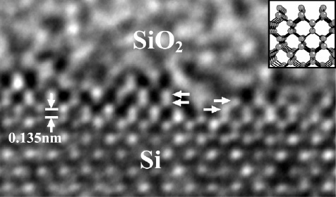
200 kV Cs-corrected TEM image of an interface between silicon and silicon oxide. Clear images of the top surface without Fresnel fringes were obtained (reprinted with permission from Japanese Scientific Monthly 05-08 (2005) 621, © 2005, JSPS).
The second new result obtained by Cs-corrected TEM is for glassy metals such as Pd–Ni–P prepared by a melt-spun method. It is believed from the results of previous TEM studies and neutron diffraction studies that medium-range-order (MRO) structures exist that float in amorphous matrices. Because there are no Fresnel fringes generated by defocusing in Cs-corrected TEM, these MRO structures become clearly visible, as shown in figure 5 [11].
Figure 5.
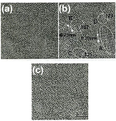
200 kV Cs-corrected TEM images of Pd-Ni-P metallic glass, showing the medium-range-order (MRO) state near the in-focus image. Cs=2 μm and Δf∼ (a) 1 nm, (b) 5 nm, and (c) 9 nm. A, B, C and D indicate MRO clusters [11] (Reprinted with permission from Phys. Rev. B 73 (2006) 012205, © 2006, The American Physical Society).
Discrimination of elements by Cs-corrected TEM
In Cs-corrected high-resolution TEM (HRTEM) images, scattering waves with sufficiently large angles are used for image formation. The minute differences in the atomic scattering factors between elements can be visualized in the image intensity. Figure 6 shows a cross-sectional image of a thin edge of a GaAs crystal observed in the [110] direction. Black dots correspond to the atomic columns comprising the crystal. In the images, one can observe slight differences in the size of the black dots originating from the difference in the atomic numbers of Ga and As atoms through the difference in their atomic scattering factors, fGa and fAs [12].
Figure 6.
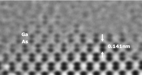
200 kV Cs-corrected TEM image of a thin area of GaAs crystal observed along [011] direction. The difference of 2 between the atomic numbers (Ga=31, As=33) is discriminated [12].
Figure 7 shows another example of the discrimination of elements; AlCuCo and AlNiCo decagonal quasi-crystals observed along the 5-fold axis using a 200 kV conventional STEM, a Cs-corrected STEM and a Cs-corrected TEM[13, 14]. The Cs-corrected STEM reveals the positions of Al atomic columns, but the image contrast is not strong. However, the Cs-corrected TEM image of the same sample clearly shows the positions of Al columns.
Figure 7.
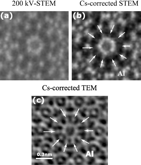
Comparison of images of AlCuCo and AlNiCo decagonal quasi-crystals using 200 kV ordinary and Cs-corrected STEM and Cs-corrected TEM. Al atoms can be visualized by Cs correction [13] ((c): reprinted with permission from Proc. IMC16, 1777, © 2006, Japan Society of Microscopy).
Figure 8 shows a third example of the discrimination of elements, that is, the detection of oxygen atomic columns in a [110] oriented magnesium oxide (MgO) crystal. A thin film of less than 5 nm thickness was prepared by vacuum deposition onto (011)-facetted crystals of sodium chloride. Furthermore, the central area was sputtered using an electron beam inside the TEM. The thickness of the area is approximately one or two unit cells of MgO (110) planes. We can identify Mg atomic columns throughout the area and also the oxygen columns between them [15]. In this observation, we have chosen a positive Cs value in contrast with the data obtained by the Juelich group for SrTiO3 crystals [16]. The present image shows the distribution of the image contrast, which may be connected with the distribution of projected potentials along the oxygen atomic columns under appropriate imaging conditions. Images obtained by the Juelich group are only sharp peaks resulting from the channeling phenomenon of electrons along the highly-symmetrical crystal axis [16].
Figure 8.
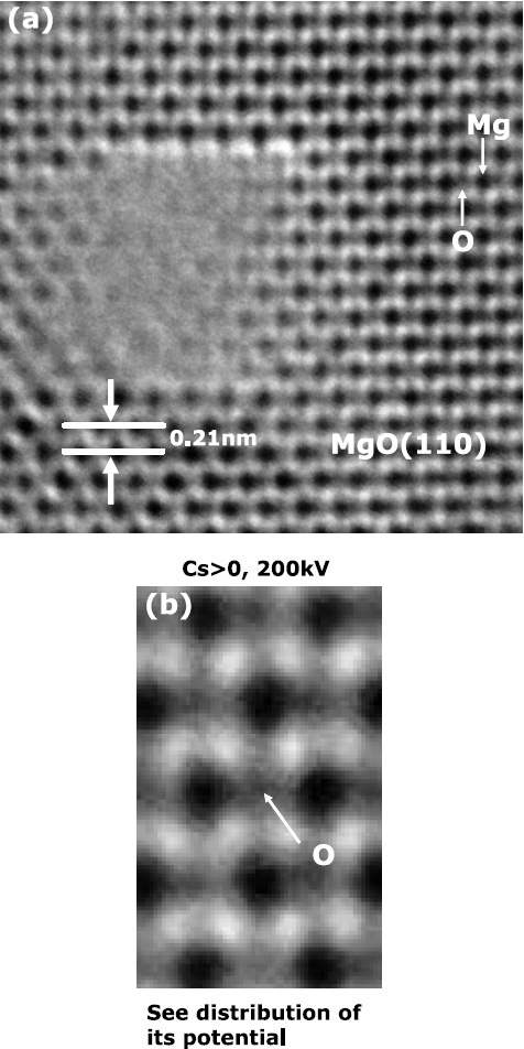
Images of oxygen (Z=8) atoms in a [011] MgO crystal (Reprinted with permission from Proc. Microsc. Microanal. 2004, p 982, © 2004, Cambridge University Press).
Removal of nonlinear image contrast by subtraction method
Phase contrast images in HRTEM are formed by the interference of a direct wave with the diffracted wave when the sample is a crystal. Up to now, we have mostly used linear terms formed by the interference between the direct wave and the corresponding diffracted wave based on the Fourier imaging principle. The point-to-point resolution of conventional TEM was around 0.2 nm, and the nonlinear interference fringes such as half-spacing lattice fringes did not disturb the image contrast because these fringes were not imaged due to the chromatic damping of the contrast transfer function, as explained by formula (2). After the Cs correction, TEM has a resolution of less than 0.1 nm, and then the half-spacing fringes such as those of gold 400 spacing appear strongly in the image intensity. It has become necessary to remove or decrease the nonlinear contrast for accurate image interpretation.
We are studying the image formation process in Cs-corrected HRTEM and have developed a new method based on the subtraction of two images obtained by Cs-corrected TEM [17]. Figure 9 shows an example of images before and after the subtraction. Artificial image contrast that does not correspond the actual atomic columns is completely removed by image subtraction. Furthermore, we have developed a newly revised image-deconvolution method using a Wiener filter to recover the transmission of image information by the objective lens at lower spatial frequencies. By the combined use of the subtraction and deconvolution methods, we succeeded in obtaining TEM images that closely corresponded to the actual projected structure of the crystals. An image-processing package based on these methods will soon be available to researchers of electron microscopy. It was also proved theoretically to the second order that the present subtraction method can even be applied to amorphous samples upon assuming the phase object approximation.
Figure 9.
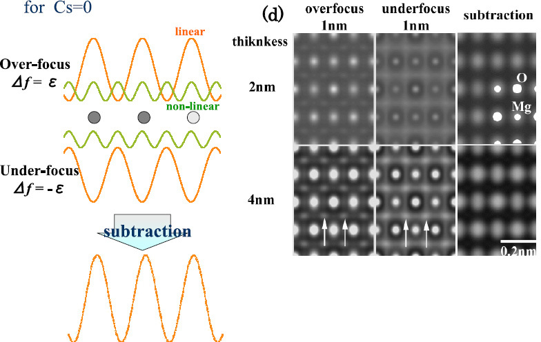
Newly developed image-subtraction method for decreasing nonlinear image contrast [15].
What is the ultimate point-to-point resolution after the establishment of Cs and Cc corrections as well as monochromators in an electron gun and effective image- processing software? Lentzen and Urban calculated the size limit of exit wave functions for silicon and germanium crystals to be 0.06 nm at 200 kV on the basis of quantum mechanics [18]. For imaging using an electron lens, the resolution may be larger than this value. The point-to-point resolution of 0.078 nm has been obtained for Si (112) crystals using a non-Cs-corrected 300 kV TEM and advanced image-processing software. Can we expect to obtain experimental results surpassing the above limitation using Cs-corrected TEMs?
Another method of reducing the nonlinear image contrast is the adoption of negative Cs values, as proposed by the Juelich group [16]. In this case, an ordinary linear term has a positive contrast (white contrast in a bright-field image), which is in agreement with white nonlinear image contrast. In that case, the nonlinear contrast introduces less complication into the linear contrast.
Z-slice imaging by Cs-corrected TEM
Application to single-wall carbon nanotubes and Pt-Rh chain molecules
Three-dimensional (3D) electron microscopy, so-called electron tomography, is one of the hot topics of recent advanced electron microscopy, particularly toward atomic resolution. For this purpose, there are two reported methods for data collection: (1) computed tomography by tilting samples based on the back-projection algorithm, and (2) z-slice imaging experimentally proposed by Borisevich et al in annular dark-field STEM [19].
We have performed another trial of z-slice imaging by Cs-corrected TEM. Figure 10 shows a high-resolution TEM image of a multiwall carbon nanotube, where lattice fringes of 0.24 and 0.14 nm are resolved due to the improvement in resolution by the Cs corrector [20]. However, the image is not essentially different from those in previous papers because the lattice fringes are overlapped or Moire fringes originate from the upper and lower multilayers of the nanotube. To observe detailed structures such as defect structures inside a graphene sheet, we need to image the structures of the upper and lower sheets separately in a single-wall carbon nanotube (SWCNT). For this purpose, we have investigated a new method of z-slicing in Cs-corrected TEM. The principle is a simple one based on the Fourier images studied by Cowley and Moodie [9]. The image contrast of a phase grating in TEM is expressed in the Fourier images, whose period of image intensity variation is written as
where d is the spacing of the phase grating. In the Fourier images, the image contrast at just-focus is zero, in the overfocused condition of the above value of formula (4), that is, a wave field beneath the sample is observed, the contrast is white, and in the underfocused condition, the contrast is black. To resolve hexagons with a spacing of 0.14 nm in a graphene layer, the Fourier period becomes about 3 nm at an accelerating voltage of 120 kV. When we prepare an SWCNT of less than 3 nm diameter, we will be able to focus the upper or lower graphene sheets individually to obtain the maximum contrast. On the basis of this consideration, we attempted to observe an SWCNT. In figures 11(a) and (b), the directions of the arrays of hexagons are different from each other. The image contrast agrees with that of a structural model determined in advance using nanobeam electron diffraction [21].
Figure 10.
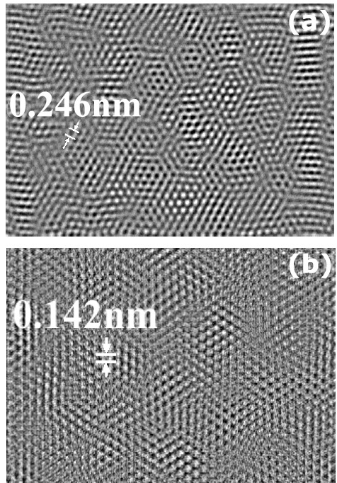
Visualization of smallest lattice spacing of graphene sheets in multiwall carbon nanotubes. (a) and (b) are images with different amounts of defocus [20].
Figure 11.
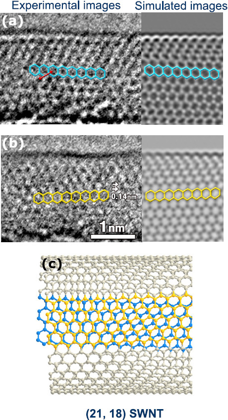
Cs-corrected TEM images of hexagons of carbons in an SWCNT. (a, b) Separate images of upper and lower planes in SWCNT and (c) the atomic model [21].
On the basis of the above successful result, we observed single molecular chains composed of platinum and rhodium atoms, as shown in figure 12. The molecules are dispersed on a thin single crystalline vacuum-deposited film of magnesium oxide (MgO) using a polar solvent [22].
Figure 12.
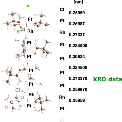
Atomic arrangement of a 1D Pt-Rh chainlike molecule (reprinted with permission from Proc. IMC16, 598, © 2006, Japan Society of Microscopy).
Figure 13 shows high-resolution images of a chain molecule on a MgO film. The fringes in the background are (200) lattice fringes with 0.21 nm spacing. Using the fringes, we calibrated the direct magnification of the images, and accurately measured the spacing between the black dots in the image. The figures attached are in good agreement with those determined by x-ray diffraction. By developing this technique, we may be able to three-dimensionally resolve the molecules tilted in the direction of the incident electrons.
Figure 13.
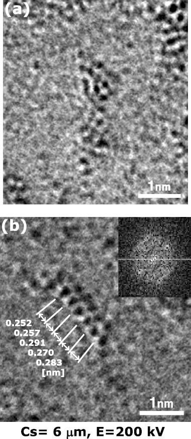
Cs-corrected TEM images of a Pt–Rh molecule supported on an MgO thin film. Images (a) and (b) are obtained from different molecules located on the MgO film (reprinted with permission from Proc. IMC16, 598, © 2006, Japan Society of Microscopy).
Figure 14 shows a series of stacked simulated TEM images of a Pt-Rh molecule along the z-direction [23]. The depth resolution using an STEM probe is usually expressed by a formula similar to the intensity distribution at focal points in optical microscopes given in the Born and Wolf textbook [24] as
where α is the convergence angle of incident rays. In the present case, the situation is, however, the phase-contrast imaging of a phase grating. Decreasing spacing observed, the depth resolution decreases to less than 2 nm, resulting in the carbon-carbon bond being resolved in one layer of hexagons of the SWCNT. This value of depth resolution is comparable to that attainable by Cs-corrected annular dark field-STEM, which was calculated by using formula (5) by Borisevich et al [19].
Figure 14.
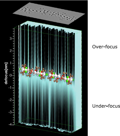
Series of simulated images stacked in the vertical direction of a Pt-Rh molecule for various amounts of defocus (reprinted with permission from Proc. Microsc. Microanal. 2007,p 890, © 2007, Cambridge University Press).
Development of new Cs-corrected selected-area electron diffraction technique
The other advantage of Cs-corrected TEM is the decrease in the positional error in selected-area electron diffraction. As is often stated in textbooks on electron microscopy, selected-area electron diffraction has positional errors depending on the diffraction angles of the spots, because the selected-area aperture is located on images enlarged by an objective lens. Images formed by higher-index diffracted waves are shifted due to the spherical aberration of the objective lens. In Cs-corrected TEM, it has become possible to obtain nm-area diffraction patterns without positional errors if we can fabricate a smaller selected-area aperture of less than 1 μm diameter [25]. The size for the diffraction pattern corresponds to less than 10 nm because the magnification of the ordinary objective lens is about 100. We have prepared a smaller selected-area aperture of about 0.4 μm by fabrication using ion etching. Figure 15(a) shows an image of a selected-area aperture inserted on silicon lattice fringes with a spacing of 0.31 nm. By using a smaller aperture in the Cs-corrected TEM, the analysis of individual stacking faults in silicon crystals has become possible with more parallel incident beams than those in the conventional nanobeam electron diffraction method [26]. This technique offers another advantage for diffraction imaging by the oversampling technique. In the oversampling technique, we need an area where the image intensity is already known. In previous studies, vacuum areas were chosen by Zuo et al, when the sample was a carbon nanotube [27]. The oversampling cannot, however, be applied for crystalline samples and thin films. The present technique solves this problem. We can set the outside area where the image intensity is known using the present smaller selected-area aperture. The image intensity of the area is exactly zero, as shown in figure 15(a). Also the selected-area diffraction method gives sharp and well-defined diffraction spots, which contributes to the feasibility of phase reconstruction by the diffractive imaging algorithm.
Figure 15.
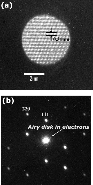
5 nm selected area nanodiffraction pattern obtained from a Si crystal in a 200 kV Cs-corrected TEM; (a) image with aperture and (b) diffraction pattern [26].
Figure 16 shows a comparison of spatial coherence between nanobeam diffraction and Cs-corrected selected-area electron diffraction obtained from the intensity distribution of an Airy disk [28, 29]. Because of the more parallel incident beam in the present method, the intensity variation is more pronounced.
Figure 16.
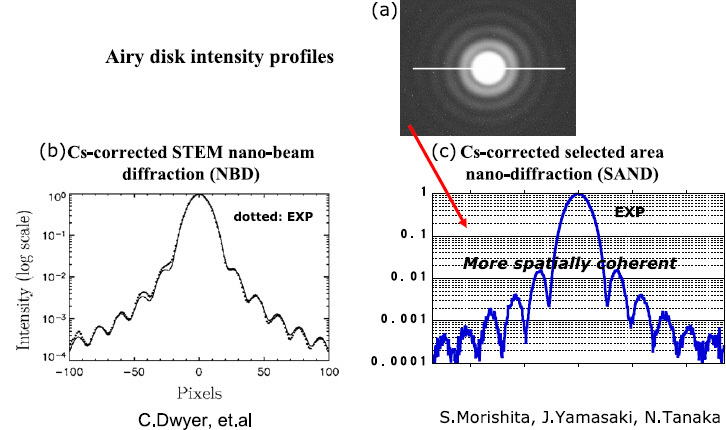
Comparison of the intensity distribution of Airy disk showing coherence; (a) Cs-corrected STEM method [29] (reprinted with permission from Appl. Phys. Lett. 90 (2007) 151104, © 2007, American Institute of Physics) and (b) Cs-corrected TEM method [28].
Advantages of Cs-corrected STEM
The advantages of Cs-corrected STEM are easily understood from the viewpoint of the forming lens of the probe [5]. The aberration correction allows the lens to be used with wider convergence angles of electron waves; thus, the probe size can be decreased according to the principle of Fourier transform, and probe current becomes larger than that in conventional STEM. This improvement is easily seen in the Ronchigram obtained as shadow images, in which a diffraction pattern is obtained using a stationary incident probe without objective (condenser) apertures [3]. The flat area with equal phases in the center can be extended from about 10 mrad to about 40 mrad at 200 kV using the Cs corrector. The decreased probe size allows high-resolution STEM images of less than 0.1 nm point-to-point resolution to be obtained, and the brighter probe minimizes the analysis time for various types of advanced material samples such as semiconductors. Figure 17 shows a characteristic example of the dynamic observation of the movement of antimony dopant atoms in silicon crystals [30]. The series of images was recorded with intervals of 11 s. We detected the jumping process of impurity atoms in the series of images. The mechanism of the jumping process is now being studied using various diffusion models. At present, thermal agitation excited by incident electrons appears to mainly contribute to the jumping.
Figure 17.

Series of Cs-corrected STEM images showing jumping process of an antimony atom in a silicon crystal [30] (reprinted with permission from Proc. Microsc. Microanal. 2007, p 1186, © 2007, Cambridge University Press).
Three-dimensional observation of atomic objects in STEM
As already discussed in section 2.5, 3D atomic observation is one of the next targets in electron microscopy. The conventional 3D electron tomography method is applicable to STEM as well as TEM. In particular, Annular dark field (ADF)-STEM images provide information on the distribution of atoms through scattering contrast (Z-contrast); thus, we may use a signal more directly connected to the 3D reconstruction of atomic objects. In TEM, the strong dynamical diffraction and crystalline diffraction are obstacles preventing the direct correspondence between atomic density and image contrast. Borisevich et al proposed a Z-scanning method by ADF-STEM by changing the focus of the STEM probe in samples [19]. This may work well if the sample consists of atomic clusters and impurity atoms embedded in amorphous films, but it does not work for crystalline samples including various types of defects and inclusions. Figure 18 shows the data we obtained by observing platinum atoms embedded in an amorphous carbon film. Because of the high sensitivity of the Z-contract STEM method, even single platinum atoms are clearly imaged [31]. The sample is ideal for studying the possibility of the 3D observation of atomic objects by ADF-STEM.
Figure 18.
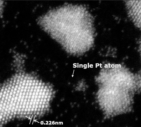
Cs-corrected STEM image of single platinum atoms and clusters in an amorphous carbon film [31]. The spacing of 0.226 nm is of the (111) lattice fringes in a platinum crystal [31].
The depth resolution is expressed by formula (5). Because of Cs correction and the use of wider convergence angles, the depth resolution of the focusing probe is markedly decreased.
Figure 19 shows data comparing (a) an uncorrected 100 kV instrument, (b) a C3-corrected 300 kV microscope, and (c) a C3/C5-corrected hypothetical 200 kV instrument from the viewpoint of the elongation of the probe in the z-direction [19]. The blurring of the depth resolution for crystalline samples is a future issue to be studied, that involves dynamical diffraction and channeling effects. Indeed, the ease of elemental analysis by EDX and EELS in a Cs-corrected STEM is greatly improved. The elemental analysis of a silicon device requires half a day less work than previously.
Figure 19.
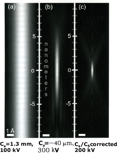
Simulated intensity profiles of electron probes along z-direction for z-slice images by conventional and Cs-corrected STEM [19] (reprinted with permission from J. Electron Microsc. 55 2006 7, © 2006, Japan Society of Microscopy).
Summary and future prospects
In this paper, the present status of Cs-corrected TEM/STEM is reviewed from the viewpoint of the observation of nanomaterials. Characteristic features in TEM and STEM are described using experimental images obtained by our group as well as data published by other groups. Cs correction up to the 3rd-order aberration has already been established and research interest is focused on correcting the 5th-order spherical aberration and chromatic aberration of the objective lens in combination with the development of a monochromator below an electron gun. To obtain ultrahigh resolution images with less than 0.07 nm point-to-point resolution, mechanical and electrical instabilities, so-called incoherent aberrations, which induce damping characteristics in transfer functions, are critical issues to be resolved. The highest recorded point-to-point resolutions, as of August 2007 are 0.078 nm using (112)-oriented Si crystals for TEM [32] and 0.063 nm using (112) GaN for STEM [33].
Another area of fundamental interest is the limitation of resolution in TEM and STEM from the quantum mechanics viewpoint. The minimum size of the exit wave function below the samples is determined from a scattering calculation where a single atom or a crystal scatters an incident wave function by finite angles.
One of the future prospects of Cs-corrected TEM/STEM is related to another of its advantages not discussed in the present paper. That is, the possible extension of space around the sample holder by correcting the chromatic and spherical aberrations. In comparison with the previous pole piece of the objective lens, one can use wider-gap pole pieces while obtaining the same resolution. This wider space will contribute to the ease of performing in situ experiments and various combinations of TEM and other analysis methods. Furthermore, we need to develop different types of in situ observation tools using the wider area. High-resolution, in situ dynamic and 3D observations are the most important keywords in the next decade of high-resolution electron microscopy.
Acknowledgments
The author would like to express his sincere thanks to many coworkers including Drs J Yamasaki, K Saitoh, S P Cho, H Sawada, E Okunishi and K Yoshida. Also Drs M Haider and P Hartel of CEOS GmbH are appreciated for their kind technological support of Cs correctors. Professor Y Ikuhara and Dr T Hirayama are acknowledged by the author for their kind collaboration in Cs-corrected TEM experiments. This work is partly supported by Grants-in-Aid in Scientific Research from MEXT, Japan and a special CREST Coordination Grant from JST, Japan.
Footnotes
Invited paper.
References
- Jenkins R and Snyder R L. 1996. Introduction to X-ray Powder DiffractometryNew York: Wiley [Google Scholar]
- Hill R J. The Rietveld Method. In: Young R A, editor. Oxford: Oxford University Press; 1993. [Google Scholar]
- Spence J C H. 3rd edn. Oxford: Oxford University Press; 2003. High Resolution Electron Microscopy. [Google Scholar]
- Haider M, Rose H, Uhlemann S, Kabius B. and Urban K. J. Electron Microsc. 1998;47:395. doi: 10.1093/jmicro/dfp021. [DOI] [PubMed] [Google Scholar]
- Krivanek O L, Dellby N. and Lupini A R. Ultramicroscopy. 1998;78:1. doi: 10.1016/S0304-3991(99)00013-3. [DOI] [Google Scholar]
- Saitoh K and Tanaka N. 2008. in preparation [Google Scholar]
- Saitoh K and Tanaka N. 2008. in preparation [Google Scholar]
- Scherzer O. J. Appl. Phys. 1949;20:20. doi: 10.1063/1.1698233. [DOI] [Google Scholar]
- Cowley J M and Moodie A F. 1957. Proc. Phys. Soc. B 70 486 10.1088/0370-1301/70/5/305 [DOI] [Google Scholar]
- Tanaka N, Yamasaki J, Usuda K. and Ikarashi N. J. Electron Microsc. 2003;52:69. doi: 10.1093/jmicro/52.1.69. [DOI] [PubMed] [Google Scholar]
- Hirotsu Y, Nieh T G, Hirata A, Ohkubo T and Tanaka N. 2006. Phys. Rev. B 73 0122051 10.1103/PhysRevB.73.012205 [DOI] [Google Scholar]
- Yamasaki J and Tanaka N in preparation [Google Scholar]
- Taniguchi S and Abe E. 2008. Philos. Mag. at press [Google Scholar]
- Saitoh K, Tanaka N, Tsai A P. and Ishizuka K. Proc. IMC. 2006;16:p 1777. [Google Scholar]
- Tanaka N and Yamasaki J. 2004. Proc. Microsc. Microanal. 982CD [Google Scholar]
- Jia C L, Lentzen M. and Urban K. Science. 2003;299:870. doi: 10.1126/science.1079121. [DOI] [PubMed] [Google Scholar]
- Yamasaki J, Kawai T. and Tanaka N. J. Electron Microsc. 2005;54:209. doi: 10.1093/jmicro/dfi029. [DOI] [PubMed] [Google Scholar]
- Lentzen M and Urban K. 2006. Proc. Microsc. Microanal. 1456CD [Google Scholar]
- Borisevich A Y, Lupini A R, Travaglini S. and Pennycook S J. J. Electron Microsc. 2006;55:7. doi: 10.1093/jmicro/dfi075. [DOI] [Google Scholar]
- Tanaka N, Yamasaki J, Kawai T. and Pan H Y. Nanotechnology. 2004;15:1779. doi: 10.1088/0957-4484/15/12/015. [DOI] [PubMed] [Google Scholar]
- Hirahara K, Saitoh K, Yamasaki J. and Tanaka N. Nano Lett. 2006;6:1778. doi: 10.1021/nl060458k. [DOI] [PubMed] [Google Scholar]
- Tanaka N, Yamasaki J, Hirahara K, Uemura K. and Matsumoto K. Proc. IMC. 2006;16:598. [Google Scholar]
- Hirahara K, Yamasaki J, Saitoh K and Tanaka N. 2007. Proc. Microsc. Microanal. 840CD [Google Scholar]
- Born M and Wolf E. 1970. Principles of Optics 4th ednNewYork: Pergamon; section 8.8 [Google Scholar]
- Yamasaki J, Sawada H. and Tanaka N. J. Electron Microsc. 2005;54:123. doi: 10.1093/jmicro/dfi028. [DOI] [PubMed] [Google Scholar]
- Yamasaki J, Nakamura K, Morishita S, Kato T. and Tanaka N. Proc. IMC. 2006;16:1020. [Google Scholar]
- Zuo J H, Vartanyants I, Gaa M, Zhang R. and Nagahara L A. Science. 2003;300:1419. doi: 10.1126/science.1083887. [DOI] [PubMed] [Google Scholar]
- Morishita S, Yamasaki J and Tanaka N. 2008. in preparation [Google Scholar]
- Dwyer C, Kirkland A, Hatel P, Müller H. and Haider M. Appl. Phys. Lett. 2007;90:151104. doi: 10.1063/1.2721120. [DOI] [Google Scholar]
- Yamasaki J, Okunishi E, Sawada H and Tanaka N. 2007. Proc. Microsc. Microanal. 1186CD [Google Scholar]
- Yamasaki J and Tanaka N. 2008. in preparation [Google Scholar]
- O'Keefe M A. 2007. Ultramicroscopy in press [Google Scholar]
- Sawada H et al. 2007. Japan J. Appl. Phys. at press [Google Scholar]


