Abstract
Recently, it was shown that lasing from epitaxial Ge quantum dots (QDs) on Si substrates can be obtained if they are partially amorphized by Ge ion bombardment (GIB). Here, we present a model for the microscopic origin of the radiative transitions leading to enhanced photoluminescence (PL) from such GIB-QDs. We provide an energy level scheme for GIB-QDs in a crystalline Si matrix that is based on atomistic modeling with Monte Carlo (MC) analysis and density functional theory (DFT). The level scheme is consistent with a broad variety of PL experiments performed on as-grown and annealed GIB-QDs. Our results show that an extended point defect consisting of a split-[110] self-interstitial surrounded by a distorted crystal lattice of about 45 atoms leads to electronic states at the Γ-point of the Brillouin zone well below the conduction band minimum of crystalline Ge. Such defects in Ge QDs allow direct transitions of electrons localized at the split-interstitial with holes confined in the Ge QD. We identify the relevant growth and annealing parameters that will let GIB-QDs be employed as an efficient laser active medium.
Keywords: Silicon photonics, quantum dots, photoluminescence spectroscopy, density functional theory, defect engineering
The use of light instead of electrical current as a means of interconnect in Si-based microelectronics will allow for a drastic reduction in heat waste and energy consumption. A number of optical components1−3 such as waveguides, detectors,4 and modulators5 are nowadays produced compatible with Si integration technology. Within Si photonics research, the optical component that certainly was and still is most difficult to obtain is a laser that can be integrated monolithically with standard Si technology for at room temperature operation. Over the past few years, progress has been made, including lasing from III–V quantum dots (QD) bonded to,6 or grown7 on Si, utilizing Ge virtual substrates. Meanwhile, the growth of III–V QD lasers on Si has been demonstrated,8,9 as well as GeSn lasers on Ge that operate at cryogenic temperatures.10 However, both device types require the growth of several micrometer-thick epilayers. These are necessary to accommodate the misfit strain between the deposited materials and the underlying Si substrate that contains the CMOS layers.
In a recent publication, we provided strong evidence that Ge quantum dots (QDs) bombarded with Ge ions (GIB) and embedded in a crystalline Si matrix can be used as a gain material for an all-group-IV nanostructure laser operating in the 1.3 μm telecommunication band.11 Microdisk resonators containing such GIB-QDs exhibit threshold behavior as well as a superlinear increase of the integrated PL intensity (IPL) concomitant with line-width narrowing as the optical pump power (Pexc) increases.11 This monolithic solution to the long-awaited missing component of Si photonics marks a major step toward optoelectronics integration on Si for high-performance optical communication and computing applications.
In contrast to conventional SiGe nanostructures,12 the GIB-QDs show dramatically shortened carrier lifetimes down to about 0.6 ns as well as negligible thermal quenching of the photoluminescence (PL) signal up to room temperature (RT) and above.11 The activation energies (EA) for thermal quenching were found to be about 350 meV.11 With increasing Pexc, the onset of the GIB-QD-related PL shifts significantly to higher energies.11 Also, we found a power law of the integrated PL of the form IPL(Pexc) ∼ Pexcm with m = 1.11 The short carrier lifetimes, a power coefficient of m = 1, and efficient PL at RT and above are strong indicators of optically direct electron–hole recombination in GIB-QDs.
Self-organized, crystalline Ge-on-Si QDs were first fabricated in 199013,14 but never matched expectations with respect to their optical properties, mainly because Si and Ge are indirect-bandgap semiconductors. Moreover, electrons and holes are also spatially separated in these type-II heterostructures because only the holes are confined within the QDs, whereas electrons are only weakly (typically ∼60 meV) bound by strain fields in the Si surrounding the QDs.12,15−17 Thus, at temperatures around ∼100–200 K electrons can thermally escape from the strain-induced potentials, leading to quenching of the PL signal. In contrast, GIB-QDs still show pronounced PL at RT and above.11
The large EA for thermal PL quenching we found in GIB-QDs11 implies that not only holes are strongly confined within the GIB-QDs, as in the case of fully crystalline Ge-on-Si QDs, but that also electrons are highly localized within the GIB-QDs with activation energies of more than 300 meV.11
The findings in ref (11) suggest that the PL-response of the GIB-QDs results from direct optical transitions in a heterosystem that is indirect both in real and in k-space. As yet, a full understanding of the involved microscopic mechanisms is missing. Such an understanding, in turn, is pivotal to optimize the growth conditions of the GIB-QDs and to investigate their influence on the optical properties in order to further enhance their PL yield.
In this work, we analyze the effect of Ge-ion bombardment on Ge QDs in a Si matrix and derive an energy level scheme that is consistent with all the observed PL properties. For this purpose, we performed sequences of Monte Carlo (MC) quench-and-anneal steps to identify the equilibrium defect structure remaining after GIB and subsequent annealing. Density functional theory was then applied to extract the electron- and hole-wave functions and the energy levels of the extended defect structure. PL experiments performed on GIB-QDs grown and annealed under a wide range of experimental conditions corroborate the results of the simulations.
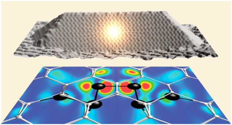
For the simulations of the defect structure of GIB-QDs, we consider the geometry and the GIB creation procedure as described in ref (11) (Figure 1). A single Ge layer was grown at a temperature of 500 °C with a coverage of 7.3 Å. The resulting Ge QDs are of hut shape with a height of about 2–3 nm bounded by {105}-facets with an inclination angle of 11.3° with respect to the Si(001) substrates14 (see TOC graphics). During QD growth, a very low dose of ∼104 Ge ions per μm2 is accelerated toward the substrate by an adjustable substrate bias VGIB in the range of 0 to −2.8 keV. This bombardment leads just to one or two hits per QD causing amorphized zones that contain one extra Ge atom (Figure 1a). During the subsequent growth of a 70 nm thick Si capping layer at temperatures ranging from 300 to 600 °C, the topmost part of the GIB-QDs recrystallizes laterally via solid-phase epitaxial regrowth (SPER),18 which then allows for overgrowth with fully crystalline Si (Figure 1b).
Figure 1.
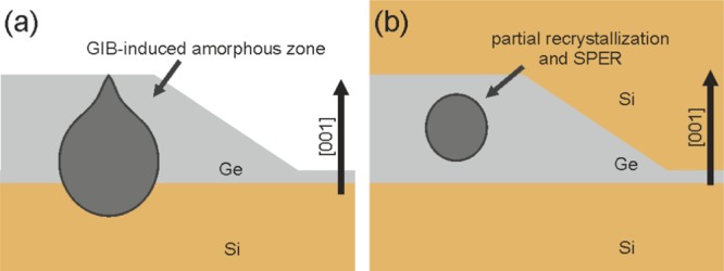
(a) Schematic view of the amorphous zone (dark gray) created in the crystalline Ge QD (gray) by low-energy implantation of a single Ge ion. (b) Partial recrystallization, solid phase epitaxial regrowth (SPER), and overgrowth of the GIB-QD with crystalline Si.
To simulate the equilibrium configuration of such a defect region with a single surplus Ge atom, we carried out a sequence of MC quench-and-anneal steps on an amorphous structure with one atom in excess of that for a perfect crystal of the same domain size. For this purpose, a 64-atom cell, composed of a rectangular grid of 2 × 2 × 2 conventional cells (Figure 2a), was joined with a region of the same volume containing 65 randomly placed atoms. Periodic boundary conditions were enforced on all sides, and an extensive series of MC quench-and-anneal steps was then carried out using the bond-switching method of Wooten, Winer, and Weaire,19 that has been successfully applied to nanocrystalline silicon before.20,21 The simulation showed an increasing crystallized fraction with the amorphous remnant eventually shrinking to approximately 45 atoms. The geometry was then relaxed using the Quantum Espresso DFT package22 with exchange and correlation effects accounted within the generalized gradient approximation (GGA) of Perdew, Burke, and Ernzerhof (PBE)23 and norm-conserving pseudopotentials. The calculations were done spin-restricted, employed a 2 × 2 × 2 k-point grid with 528 electron bands, and had an energy cutoff of 100 Ry. The geometry optimization resulted in the extended defect structure, shown in Figure 2b. This defect is known as a split-[110] interstitial,24 and it has previously been identified as having the lowest interstitial formation energy in crystalline Ge.25,26 Significantly, this core defect is surrounded by a neighborhood of gradually displaced atoms (Figures 2c and d).
Figure 2.
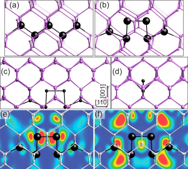
(a) Perfect Ge crystal structure, the enlarged black enlarged atoms highlight the region of interest for the subsequent formation of a split-[110] interstitial. (b) Ground state defect structure that results after computational crystallization of an amorphous state containing one extra Ge atom. The core atoms of the split-[110] interstitial are shown in black, but the positions of four surrounding atoms are significantly shifted. This effect becomes even more clear in the face-on (c) and side (d) views. (e, f) Electronic orbital electron density cross sections in the plane containing the split interstitial. (e) The CB+1 level at the Γ-point is highly localized at the defect. (f) The VB maximum at the Γ-point is slightly delocalized throughout the domain. The highest density (red) is 0.00035 electrons/bohr3, while the lowest density (blue) is 0.0 electrons/bohr3.
This remnant of the originally amorphized region causes the lowest conduction band (CB) to be shifted downward so that the gap is reduced by 72 meV. The next three CBs states above it are shifted below the original CB as well. Note that DFT results usually underestimate the energies of the band gaps (here 0.34 eV) but does so with a rigid, downward “scissors” shift of the conduction bands that accurately predicts their relative values.
Of particular interest is that the band just above the CB edge (CB+1 band) is localized at the defect at its Γ-point. This is the most physically accurate k-point in the dispersion curve since it is not influenced by replicas of the defect that are implied by periodic boundary conditions. Furthermore, the domain size is sufficiently large that the associated band structure should be quite flat in any case, and a spatially localized Kohn–Sham orbital at the Γ-point accurately portrays the tendency of electrons with this energy to be bound at the defect.
A cross section of this electronic orbital is overlaid onto the defect structure in Figure 2e. The defect also introduces a parasitic hole state 92 meV above the crystalline Ge valence band (VB) (see orange dashed line in Figure 3b, and its electron density cross section is shown in Figure 2f). Future temperature-dependent PL investigations at emission wavelengths longer than 1600 nm will be employed to study the activation and deactivation of this level. This should clarify whether at RT this hole-state can be filled with an electron and thus would hardly contribute as a recombination level for the electrons in the upper level.
Figure 3.
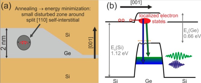
(a) Recrystallization to a split-[110] self-interstitial with surrounding lattice deformation upon annealing or overgrowth with Si at high sample temperature. (b) Proposed energy level diagram in the [001] growth direction. The full red oval depicts localized Γ-point electron-states at the defect site. The green and blue arrows show GIB-QD PL emissions of longer and shorter wavelengths, and the hole states in the GIB-QD are indicated by the green-blue-shaded area. Parasitic hole states above the VB edge of Ge are indicated by the dotted orange line.
The split-[110] self-interstitial with a surrounding lattice distortion zone has structural properties very similar to the extended point defects in ref (27). In this reference, Cowern et al. investigated a defect system in Ge crystals in which N+1 atoms are present in a volume where N atoms would create a defect-free crystal lattice. The energy of such a system—including entropy—displays two distinct minima: one for N = 1, i.e., a self-interstitial with dangling bonds (DB), and another one for N ≈ 45 atoms where in the extended point defect the bonds can be rearranged reducing the energy lost by dangling bonds at the expense of bond distortions. For 1 < N < 45 the volume cannot reconfigure the bonds in an efficient way leading to an activation barrier between the two minima. For much higher N the single additional atom only negligibly contributes to the total energy, and thus, amorphization increases the energy of the system as compared to a crystalline lattice.27 In the case of our GIB-QDs, the initially amorphized volume certainly consist of much more than 45 atoms. Thus, the energetic minimum configuration of the extended point defect will only be obtained upon recrystallization. For our situation, we interpret the defect structure in ref (27) as a split-[110] self-interstitial surrounded by a distorted lattice.
Based on this defect structure (Figure 2 and Figure 3a) and the associated energy levels from the DFT calculations, we suggest in Figure 3b an energy level scheme that is consistent with the observed experimental observations on GIB-QDs in ref (11). One should keep in mind that the observed11 PL emission energies of up to 1 eV in combination with EA values of ∼350 meV for thermal quenching of electrons and holes imposes a highly limiting constraint on plausible models for the observed behavior, given that the band gap energies of Ge and Si are 0.66 and 1.12 eV at RT, respectively. The level scheme in Figure 3b is consistent with the following experimental observations in ref (11): (i) a pronounced shift of the PL wavelength λPL to smaller values with increasing excitation power Pexc, (ii) a large EA of approximately 350 meV for electrons and holes, (iii) a power-coefficient of m = 1 for the increase of the integrated PL intensity IPL with increasing Pexc, (iv) negligible thermal-quenching of IPL at RT as compared to 20 K, and (v) the short carrier lifetimes of less than 1 ns observed for GIB-QDs.
A plausible scenario for the direct optical transition on a GIB-QD can now be posited. Electrons tunnel from the Si matrix into the deep, spatially localized states of the split-[110] self-interstitial (Figure 2e and full red oval in Figure 3b) that are induced by Ge ion bombardment (Figure 1) and partial recrystallization (Figures 1b and 3a).18 As these electrons are Γ-point states in reciprocal space they can undergo direct optical transitions by recombining with holes that are also confined at the GIB-QD (Figure 3b). Excitation of an ensemble of GIB-QDs with different sizes as well as filling of the different defect induced levels leads to the observed broad range of transition energies (green and blue arrows in Figure 3b).11 Thermal quenching will be observed if either holes escape from the GIB-QDs, or electrons at the defect site overcome an activation energy of EA ≈ 350 meV.11
In the following, we will determine the role of the thermal budget during GIB-QD formation. In Figures 1 and 3a, we indicated that the growth temperatures should have strong influence on whether we deal with an amorphous Ge core or the aforementioned minimum energy defect configuration. Immediate quenching of the temperature after Ge deposition under Ge ion bombardment will favor an amorphous cluster (Figure 1b), whereas high capping layer growth temperatures or postgrowth sample annealing will lead to the single defect (Figure 3a).
To investigate the influence of the thermal budget during growth and of the implantation depths of the excess Ge ion during GIB, we performed PL experiments on a series of ∼20 GIB-QD samples grown under identical growth conditions except for one parameter that was systematically varied. The first seven samples were annealed in situ after growth of the Si capping layer for 2 h at Tann ranging from 500 to 675 °C. For six samples, we employed variations of VGIB from 0 to −2.8 kV, and for another six samples we varied TCap from 300 to 600 °C. Finally, hydrogen passivation experiments were performed on four samples, annealed and as-grown by using a low-energy (100 eV) Kaufman source. The samples were held at 300 °C to enhance H diffusion during irradiation. The hydrogen irradiation dose was 1018 ions/cm2. For the PL experiments, we used an excitation diode laser operated at 442 nm and a microscope objective with a numerical aperture of 0.7 which is used both for laser focusing and for collecting the PL signal from the sample. The laser spot diameter on the sample was ∼2 μm. The signal is dispersed by a grating spectrometer and recorded by a nitrogen-cooled InGaAs line detector. All measurements were performed at RT.
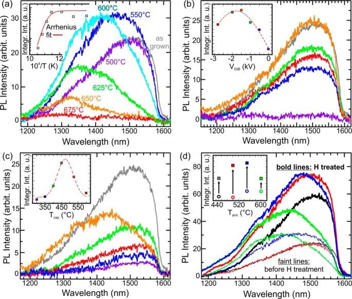
Figure 4a shows PL spectra of GIB-QDs before and after thermal annealing. Annealing at Tann = 500 °C has virtually no effect on the PL, as compared to the as-grown reference sample. At Tann of 550 and 600 °C, the PL yield is increased (Figure 4a, a finding which we attribute to improved recrystallization of the initially amorphized region (see Figure 1b) toward the energetic minimum configuration of the extended split-[110] self-interstitial (see Figures 2 and 3a). The simultaneous shift of λPL to higher energies can be attributed to enhanced intermixing between the small GIB-QDs and the surrounding Si matrix at elevated substrate temperatures.28
Figure 4.
(a) Influence of the annealing temperature Tann on the GIB-QD PL for 2 h of in situ, post growth annealing at Tann. The blue-shift of the spectra at higher Tann is attributed to enhanced intermixing of the GIB-QDs with the surrounding Si matrix. Quenching of the GIB-QD PL with increasing Tann results from migration of the extended Ge point defect out of the GIB-QD with an activation energy for diffusion ED of ∼3.33 eV as calculated from an Arrhenius plot (inset of a). (b) Influence of VGIB on the PL of the GIB QDs; the inset depicts IPL vs VGIB, revealing an optimum range for VGIB. (c) Influence of Tcap on the GIB-QD PL spectrum; The inset depicts IPL vs Tcap and an optimum range for Tcap. For too low Tcap SPER breaks down, while for too high Tcap the defect can migrate out of the QD. (d) Influence of hydrogen irradiation on the GIB-QD-PL. The faint lines show original data. Data including the reference sample (black) and three samples that were annealed after Si cap growth. Bold lines represent PL spectra after H irradiation. The inset depicts IPL before and after H treatment.
For Tann > 600 °C, IPL quenches exponentially. We fitted this decay according to
| 1 |
were I0 is the integrated PL-intensity of the as-grown sample, A is a scaling coefficient, kB is the Boltzmann constant, and ED is an activation energy for diffusion of the defect. The fit results in ED = 3.33 eV, which is in excellent agreement with the activation energies obtained by Cowern et al.27 for the migration of extended point defects. Due to the large defect structure, ED is significantly larger than the activation energy for the migration of a single self-interstitial which is about 0.42–1.45 eV.29−31
In the next experiment, we determined the optimum Ge ion energy for amorphization of our Ge QDs of ∼2 nm height. Figure 4b shows PL spectra recorded on from GIB-QDs with Ge ion acceleration voltages VGIB ranging from 0 to −2.8 kV. The maximum PL yield is observed around VGIB ≈ −1.75 kV. Without GIB (VGIB = 0) no QD PL is observed at room temperature, in agreement with previous results from undisturbed Ge QDs.12,15−17
If the ion energy becomes too high, the depth of the amorphous zone will exceed the height of the QDs. If this is the case, the implanted excess Ge ion becomes located in the Si substrate, and therefore the split-[110] self-interstitial cannot be formed in the QD. Consequently, IPL drops for too high VGIB. In general, the exact value of VGIB is not crucial (Figure 4b, as long as the projected range of the implanted Ge ions lies within the QDs.
In Figure 4c the influence of the growth temperature Tcap of the Si capping layer on the PL emission intensity is investigated. The PL yield reaches a maximum for Tcap ≈ 475 °C. For Tcap ≤ 400 °C, the IPL decreases, because the lower thermal budget prevents efficient surface recrystallization due to SPER.18 Thus, undisturbed growth of the Si capping layer on top of the samples is hampered, leading to enhanced nonradiative recombination channels in the sample. If Tcap is too high (> ≈550 °C), the extended point defect has sufficient thermal budget to migrate out of the QD28 which causes PL quenching.
It is shown in ref (32) that Ge dangling bonds (DBs) exhibit different electronic properties when compared to DBs in Si. DBs in Ge create states below the VB edge that are negatively charged. Thus, interstitial hydrogen cannot efficiently passivate DB defects, and electrons will not be localized at DB sites.32 Consequently, upon hydrogen passivation of our samples, we do not expect a quenching of IPL in GIB-QDs. Indeed, as can be seen in Figure 4d, IPL actually increases after H implantation. This can be explained by the presence of residual crystalline defects induced by GIB in the Si substrate that, in turn, can be cured by H passivation as found in other QD material systems.33 This consequently reduces the number of nonradiative recombination channels in the system and therefore increases IPL. In turn, this finding shows that H-irradiation can be a valuable means to increase the emission efficiency of GIB-QDs and hence to enhance the optoelectronic properties of these nanostructures.
Thus, far, we have established that the role of Γ-point electrons localized at the split [110]-self-interstitial defects is of major importance with respect to the extraordinary PL properties of GIB-QDs. To elucidate the role of the holes, we go back to the energy level diagram presented in Figure 3b and the DFT results of Figure 2. Evidently, the hole ground state is located in the crystalline part of the QD. To emphasize the importance of hole-confinement in the QD, we have fabricated for comparison quantum well (QW) samples where either 0.5 nm of Ge or 1 nm of Si0.3Ge0.7 were grown with the same GIB treatment as the QD samples.
In contrast to the GIB-QD PL, though, the GIB-QW PL is almost completely suppressed as can be seen in Figure 5. While the holes are efficiently trapped in the GIB-QDs, in the GIB-QW samples (or in Ge bulk samples), the holes can diffuse away from the extended split-[110] self-interstitial into the region between two such defects, as schematically depicted in Figure 5 by the blue arrow. The charge carrier separation reduces the overlap of the electron and hole wave function and thus the transition matrix element for optical transitions. Thus, quantum dots are a necessary precondition for direct optical transitions in Si/Ge heterostructures treated by Ge ion bombardment.11 In contrast, enhanced PL yields can neither be observed in GIB treated quantum well structures (Figure 5), nor in bulk Ge, where the split-[110]-self-interstitial interstitial is known for a long time.24−26
Figure 5.
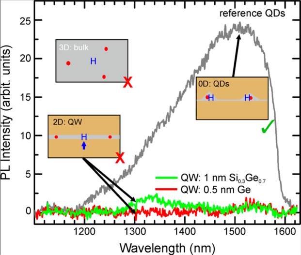
RT PL signals of GIB-QDs (gray) and two different GIB-QWs (green and red). Only the GIB QDs show strong PL enhancement. Inserts: Schematic views of GIB-QDs (right) versus a GIB-QW (lower left) and a GIB-bulk samples. Holes (blue H) are confined in the GIB-QDs and thus overlap strongly with electrons trapped at the defect-sites (red dots). In contrast, holes in a QW of in bulk Ge can diffuse away from the two point defects (blue arrow), thus reducing the electron–hole wave function overlap.
In summary, we attribute the strong and temperature-stable PL of GIB-QD samples to the formation of split-[110]-self-interstitials surrounded by local lattice distortions after Ge ion bombardment and subsequent annealing. Such GIB-QDs have already shown outstanding optical properties.11 The split-[110]-self-interstitial leads to highly localized electron states around the Γ-point deep in the band gap of the Ge QD, allowing for direct radiative recombination channels within the Ge quantum dots, which would be indirect in both real and reciprocal space without Ge ion bombardment. The DFT calculation results are corroborated by several series of experiments in which the influence of various growth parameters was investigated. The experimental results will also allow for further improvement of the PL yield in this new and promising nanostructure system. Hence, GIB-QDs have the potential to affect the developments of future integrated technology for data communication by opening a route toward all-group IV lasers that can be monolithically integrated with standard Si technology.
Acknowledgments
The authors gratefully thank G. Springholz for the allowance to use and modify the STM image of a Ge hut cluster for the table of contents graphic and G. Bauer and A. Rastelli for support. The work was supported by the Austrian Science Fund (FWF): J3328-N19 and P29137-N36.
Glossary
Abbreviations
- GIB-QDs
Ge ion bombarded quantum dots
- VGIB
Ge ion acceleration voltage
- Tcap
Si capping layer growth temperature
- Tann
sample annealing temperature
- IPL
integrated photoluminescence intensity
- λPL
photoluminescence emission wavelength
- CB
conduction band
- VB
valence band
- EA
activation energy
- PL
photoluminescence
- MBE
molecular beam epitaxy
- RT
room temperature
- DFT
density functional theory
- SPER
solid phase epitaxial regrowth
Author Contributions
M.G., M.T.L., and M.B. contributed equally. The manuscript was written through contributions of all authors.
The work was supported by the Austrian Science Fund (FWF): J3328-N19 and P29137-N36.
The authors declare no competing financial interest.
References
- Pavesi L.; Lockwood D. J.. Topics in Applied Physics 94; Springer-Verlag: Berlin, 2004. [Google Scholar]
- Soref R. IEEE J. Sel. Top. Quantum Electron. 2006, 12, 1678. 10.1109/JSTQE.2006.883151. [DOI] [Google Scholar]
- Tsybeskov L.; Lockwood D. J.; Ichikawa M. Proc. IEEE 2009, 97, 1161–1165. 10.1109/JPROC.2009.2021052. [DOI] [Google Scholar]
- Yin T.; Cohen R.; Morse M. M.; Sarid G.; Chetrit Y.; Rubin D.; Paniccia M. J. Opt. Express 2007, 15, 13965–13971. 10.1364/OE.15.013965. [DOI] [PubMed] [Google Scholar]
- Roth J. E.; Fidaner O.; Schaevitz R. K.; Kuo Y. H.; Kamins T. I.; Harris J. S.; Miller D. A. Opt. Express 2007, 15, 5851–5859. 10.1364/OE.15.005851. [DOI] [PubMed] [Google Scholar]
- Park H.; Fang A. W.; Kodama S.; Bowers J. E. Opt. Express 2005, 13, 9460–9464. 10.1364/OPEX.13.009460. [DOI] [PubMed] [Google Scholar]
- Wang T.; Liu H.; Lee A.; Pozzi F.; Seeds A. Opt. Express 2011, 19, 11381–11386. 10.1364/OE.19.011381. [DOI] [PubMed] [Google Scholar]
- Chen S.; Li W.; Wu J.; Jiang Q.; Tang M.; Shutts S.; Elliott S. N.; Sobiesierski A.; Seeds A. J.; Ross I.; Smowton P. M.; Liu H. Nat. Photonics 2016, 10, 307–311. 10.1038/nphoton.2016.21. [DOI] [Google Scholar]
- Wan Y.; Li Q.; Liu A. Y.; Gossard A. C.; Bowers J. E.; Hu E. L.; Lau K. M. Opt. Lett. 2016, 41, 1664–1667. 10.1364/OL.41.001664. [DOI] [PubMed] [Google Scholar]
- Wirths S.; Geiger R.; von den Driesch N.; Mussler G.; Stoica T.; Mantl S.; Ikonic Z.; Luysberg M.; Chiussi S.; Hartmann J. M.; Sigg H.; Faist J.; Buca D.; Grützmacher D. Nat. Photonics 2015, 9, 88. 10.1038/nphoton.2014.321. [DOI] [Google Scholar]
- Grydlik M.; Hackl F.; Groiss H.; Glaser M.; Halilovic A.; Fromherz T.; Jantsch W.; Schäffler F.; Brehm M. ACS Photonics 2016, 3, 298–303. 10.1021/acsphotonics.5b00671. [DOI] [PMC free article] [PubMed] [Google Scholar]
- Tsybeskov L.; Lockwood D. J. Proc. IEEE 2009, 97, 1284–1303. 10.1109/JPROC.2009.2020711. [DOI] [Google Scholar]
- Eaglesham D. J.; Cerullo M. Phys. Rev. Lett. 1990, 64, 1943. 10.1103/PhysRevLett.64.1943. [DOI] [PubMed] [Google Scholar]
- Mo Y.-W.; Swartzentruber B. S.; Lagally M. G. Phys. Rev. Lett. 1990, 65, 1020–1023. 10.1103/PhysRevLett.65.1020. [DOI] [PubMed] [Google Scholar]
- Fukatsu S.; Sunamura H.; Shiraki Y.; Komiyama S. Appl. Phys. Lett. 1997, 71, 258. 10.1063/1.119514. [DOI] [Google Scholar]
- Dashiell M. W.; Denker U.; Schmidt O. G. Appl. Phys. Lett. 2001, 79, 2261–2263. 10.1063/1.1405148. [DOI] [Google Scholar]
- Brehm M.; Suzuki T.; Fromherz T.; Zhong Z.; Hrauda N.; Hackl F.; Stangl J.; Schäffler F.; Bauer G. New J. Phys. 2009, 11, 063021. 10.1088/1367-2630/11/6/063021. [DOI] [Google Scholar]
- Williams J. S. Nucl. Instrum. Methods Phys. Res. 1983, 209, 219–228. 10.1016/0167-5087(83)90803-7. [DOI] [Google Scholar]
- Wooten F.; Winer K.; Weaire D. Phys. Rev. Lett. 1985, 54, 1392. 10.1103/PhysRevLett.54.1392. [DOI] [PubMed] [Google Scholar]
- Lusk M. T.; Collins R. T.; Nourbakhsh Z.; Akbarzadeh H. Phys. Rev. B: Condens. Matter Mater. Phys. 2014, 89, 075433. 10.1103/PhysRevB.89.075433. [DOI] [Google Scholar]
- Bagolini L.; Mattoni A.; Collins R. T.; Lusk M. T. J. Phys. Chem. C 2014, 118, 13417–13423. 10.1021/jp5024586. [DOI] [Google Scholar]
- Giannozzi P.; Baroni S.; Bonini N.; Calandra M.; Car R.; Cavazzoni C.; et al. J. Phys.: Condens. Matter 2009, 21, 395502. 10.1088/0953-8984/21/39/395502. [DOI] [PubMed] [Google Scholar]
- Perdew J. P.; Burke K.; Ernzerhof M. Phys. Rev. Lett. 1996, 77, 3865–3868. 10.1103/PhysRevLett.77.3865. [DOI] [PubMed] [Google Scholar]
- Blöchl P. E.; Smargiassi E.; Car R.; Laks D. B.; Andreoni W.; Pantelides S. T. Phys. Rev. Lett. 1993, 70, 2435. 10.1103/PhysRevLett.70.2435. [DOI] [PubMed] [Google Scholar]
- da Silva A. J. R.; Janotti A.; Fazzio A.; Baierle R. J.; Mota R. Phys. Rev. B: Condens. Matter Mater. Phys. 2000, 62, 9903. 10.1103/PhysRevB.62.9903. [DOI] [Google Scholar]
- Dionízio Moreira M.; Miwa R. H.; Venezuela P. Phys. Rev. B: Condens. Matter Mater. Phys. 2004, 70, 115215. 10.1103/PhysRevB.70.115215. [DOI] [Google Scholar]
- Cowern N. E. B.; Simdyankin S.; Ahn C.; Bennett N. S.; Goss J. P.; Hartmann J.-M.; Pakfar A.; Hamm S.; Valentin J.; Napolitani E.; De Salvador D.; Bruno E.; Mirabella S. Phys. Rev. Lett. 2013, 110, 155501. 10.1103/PhysRevLett.110.155501. [DOI] [PubMed] [Google Scholar]
- Brehm M.; Grydlik M.; Groiss H.; Hackl F.; Schäffler F.; Fromherz T.; Bauer G. J. Appl. Phys. 2011, 109, 123505. 10.1063/1.3594693. [DOI] [PubMed] [Google Scholar]
- Śpiewak P.; Muzyk M.; Kurzydłowski K. J.; Vanhellemont J.; Młynarczyk K.; Wabiński P.; Romandic I. J. Cryst. Growth 2007, 303, 12–17. 10.1016/j.jcrysgro.2006.11.316. [DOI] [Google Scholar]
- Ding K.; Andersen H. C. Phys. Rev. B: Condens. Matter Mater. Phys. 1986, 34, 6987. 10.1103/PhysRevB.34.6987. [DOI] [PubMed] [Google Scholar]
- Khoo G. S.; Ong C. K. J. Phys. Chem. Solids 1990, 51, 1177–1179. 10.1016/0022-3697(90)90098-Z. [DOI] [Google Scholar]
- Weber J. R.; Janotti A.; Van de Walle C. G. Phys. Rev. B: Condens. Matter Mater. Phys. 2013, 87, 035203. 10.1103/PhysRevB.87.035203. [DOI] [Google Scholar]
- Polimeni A.; Marangio D.; Capizzi M.; Frova A.; Martelli F. Appl. Phys. Lett. 1994, 65, 1254. 10.1063/1.112087. [DOI] [Google Scholar]


