Abstract
Structural and electronic properties of two-dimensional stanene and graphene heterostructure (Sn/G) are studied by using first-principles calculations. Various supercell models are constructed in order to reduce the strain induced by the lattice mismatch. The results show that stanene interacts overall weakly with graphene via van der Waals (vdW) interactions. Multiple phases of different crystalline orientation of stanene and graphene could coexist at room temperature. Moreover, interlayer interactions in stanene and graphene heterostructure can induce tunable band gaps at stanene’s Dirac point, and weak p-type and n-type doping of stanene and graphene, respectively, generating a small amount of electron transfer from stanene to graphene. Interestingly, for model , there emerges a band gap about 34 meV overall the band structure, indicating it shows semiconductor feature.
Keywords: First-principles, Stanene, Graphene, Heterostructure, Structural properties
Background
Two-dimensional (2D) materials, such as graphene [1–6], silicene [7–13], germanene [14–16], hexagonal boron nitride (hBN) [17, 18], and transition metal dichalcogenides (TMDs, such as MoS2) [19, 20], have received considerable attention recently because of their outstanding properties and potential applications. These 2D layers can be integrated into a multilayer stack (vertical 2D heterostructure) and have been widely studied experimentally and theoretically, such as graphene/silicene (G/Si) [21, 22], graphene/hexagonal boron nitride (G/hBN) [23, 24], silicene/HBN [25], silicene/GaS [26, 27], TMDCs/graphene [28, 29], stacked TMDCs [30, 31], phosphorene/MoS2 [32], and phosphorene/graphene [33]. The resulting artificial 2D heterostructures provide access to new properties and applications far beyond their simplex components.
Most recently, a new 2D material, stanene (the form of 2D stannum), firstly proposed by Liu et al. [34], has been mentioned as a host material for topological insulator (TI), which are new states of quantum matter with an insulating bandgap in the bulk while conducting states at the edges and protected by time reversal symmetry [35–40]. For instance, stanene and its derivatives could support a large-gap 2D quantum spin Hall (QSH) state and thus enable the dissipation less electric conduction at room temperature. Moreover, stanene could also provide enhanced thermoelectricity [41], topological superconductivity [42], and the near-room-temperature quantum anomalous Hall (QAH) effect [43]. Zhu et al. [41] have reported the successful fabrication of 2D stanene with metallic features on the Bi2Te3 (111) substrate by molecular beam epitaxy (MBE). Xu et al. [44] found that varying substrate conditions AB(111), where A = Pb, Sr, Ba and B = Se, Te, considerably tunes electronic properties of stanene, and the supported stanene gives either trivial or QSH states, with significant Rashba splitting induced by inversion asymmetry.
Technically, it is possible to fabricate a heterostructure of stanene on a suitable substrate, in order to form honeycomb-like bilayer atomic structure. Stanene has a hexagonal lattice, as well as the requirement of lattice status of the substrate. The lattice mismatch between the substrate and the stanene should be small, and it should be energetically favorable to stanene to grow in a quasi-two-dimensional growth mode. As one of the popular 2D materials, we propose a question whether stanene can grow on a graphene substrate or stanene/graphene (Sn/G) can form a 2D heterostructure with promising structural and electronic properties.
In this work, we design a new 2D stanene/graphene heterostructure and study its geometric and electronic properties by using first-principles calculations. The results show that stanene interacts overall weakly with graphene via vdW interactions. Therefore, their intrinsic electronic properties can be preserved in stanene/graphene heterostructure. Moreover, interlayer interactions in stanene/graphene heterostructure can induce tunable band gaps at stanene’s Dirac point, and weak p-type and n-type doping of stanene and graphene, respectively. Our paper is organized as follows. In the “Methods” section, we describe the details of computational methods. The results and discussions are presented in the “Results and Discussion” section. Finally, a brief summary is summarized in the “Conclusions” section.
Methods
Our theoretical calculations are performed in the framework of density functional theory (DFT) [45] as implemented in the Vienna ab initio simulation package (VASP) [46]. Valence wave functions are treated by the projector augmented wave (PAW) [47, 48] method that uses pseudopotential operators but keeps the full all-electron wave functions. The interlayer interaction is checked by various exchange-correlation energy functionals, including the local density approximation (LDA) [49], the Perdew–Burke–Ernzerhof (PBE) [50] generalized gradient approximation (GGA), and the PBE with vdW corrections: the vdW-D2 functionals [51]. The plane-wave energy cutoff is set to be 400 eV. We have checked the convergence of k points, and a 5 × 5 × 1 k-sampling generated by the Monkhorst–Pack scheme [52] with Gamma centered for the Brillouin zone is adopted. The structural optimization is allowed to relaxed until the maximum force on each atom becomes at least less than 0.01 eV/Å and the maximum energy change between two steps is smaller than 10−5 eV. A vacuum layer of at least 20 Å is used.
Results and Discussion
Geometry and Energetics of Stanene/Graphene
For the monolayer graphene and free-standing low-buckled stanene, the lattice constants we obtained from LDA are 2.45 and 4.56 Å, respectively, which agree well with the reported values of 2.46 and 4.67 Å for graphene and stanene, respectively [53, 54]. Note that the lattice mismatch is as large as 7% even when a supercell consisting of 2 × 2 lateral periodicity of graphene and 1 × 1 stanene is employed. And the matched structure usually forms when the mismatch is small. An appropriate supercell in the bilayer system can be obtained by inducing relative rotations between the stanene and graphene substrates. For a 2D hexagonal lattice, it can be realized to get various lattice angles by longer lattice vectors from the primitive unit cell. For example, the angles corresponding to the lattice vectors for , , , , , , and unit cells are 30°, 19.1°, 13.9°, 10.9°, 9.0°, 5.8°, and 15.3°, respectively.
The heterostructures along with their structural parameters are listed in Table 1. Taking the for Sn/G as an example, it corresponds to a heterostructure consisting of 3 × 3 stanene unit cell and graphene unit cell combined by a relative rotation of angle α equal to 9. This configuration will be represented as below.
Table 1.
Heterostructure configurations for the stanene/graphene bilayers (abbreviated as Sn/G)
| Sn/G | a (Å) | α (°) | θ (°) | Δ (Å) | L Sn | L G | L Sn/G | Mismatch (%) | Strain (%) | E b (meV) |
|---|---|---|---|---|---|---|---|---|---|---|
| 4.53 | 9 | 111.2 | 0.84 | 13.68 | 13.61 | 13.62 | 0.07 | −0.4 | −76 | |
| 4.55 | 3.8 | 111.3 | 0.82 | 24.12 | 24.07 | 24.07 | 0.29 | −0.2 | −77 | |
| 4.56 | 5.1 | 111.3 | 0.82 | 20.89 | 20.88 | 20.87 | 0.48 | −0.1 | −78 | |
| 4.61 | 19.1 | 112.2 | 0.80 | 12.06 | 12.22 | 12.20 | 1.8 | 1.1 | −72 | |
| 4.68 | 16.1 | 112.2 | 0.80 | 16.43 | 16.93 | 16.89 | 3.6 | 2.8 | −57 |
Each configuration is built by combining different supercells in individual layers with a relative rotational angle α between them. L Sn/G is the lattice constant of the relaxed bilayer heterostructure and the corresponding a is the effective lattice constant of stanene in the relaxed heterostructure, while L Sn and L G are the lattice constants for the particular unrelaxed supercells of stanene and graphene, respectively. θ and Δ are the bond angle and buckling height in stanene, respectively. The mismatch, strain, and E b are defined in the text
Figure 1 shows the atomic structure of the Sn/G bilayer heterostructure system. The yellow and red atoms represent different types of Sn atoms in the low-buckled monolayer. A Sn atom in the top layer of stanene is placed on the top of a C atom in graphene. After relaxing, the buckling height Δ is found to be 0.8 Å in this system, and the interlayer distance from graphene to the bottom Sn layer is 3.5 Å based on the LDA calculation (to be discussed below), indicating that it belongs to the class of vdW type of heterostructures.
Fig. 1.
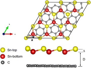
Top and side views of the heterostructure of (a heterostructure consisting of 3 × 3 stanene unit cell and graphene unit cell). Yellow, red, and gray spheres represent Sn-top, Sn-bottom, and C atoms, respectively. Δ and D represent the buckling height of stanene and interlayer distance between the substrate graphene and bottom Sn layer, respectively. The black arrows represent the lattice vector and of the unit cell of stanene and graphene
L Sn/G in Table 1 is the heterostructure length of the fully relaxed Sn/G bilayer determined by the LDA, while L Sn and L G are the lattice constants for the particular unrelaxed supercells of stanene and graphene, respectively. The lattice parameter of Sn/G heterostructure is fixed to be (L Sn + L G)/2 with a small lattice mismatch for both stanene and graphene. After fully relaxation, it is found that L Sn/G is very close to L G, which indicates that there is almost no strain in graphene layer. The lattice mismatch between the periodic unrelaxed supercell of monolayer stanene and graphene is defined as mismatch = |L Sn − L G|/L G, and it is a quite small value as shown in Table 1. The strain in the stanene layer is defined by
| 1 |
where a and a 0 are the relaxed (bilayer) and unrelaxed primitive lattice constants.
As shown in Table 1, we focus on the heterostructure models that induce a strain of less than 3%. The bond angles θ and buckling height Δ in stanene will be slightly affected by the strain as shown in Table 1. In free-standing monolayer stanene, the bond angle θ is uniform, as shown as red circle in Fig. 2. With the presence of a substrate, the bond angles exhibit a small variation of a few degrees, as the lattice symmetry is slight broken in the Sn layer. θ shown in Table 1 is the average value, and all the distributions of bond angles are shown in Fig. 2. Obviously, when the strain < 0, the stanene layer is applied by a compressive strain, which causes the bond angle θ to be slightly smaller and the buckling height Δ to be higher. There are opposite results when the strain > 0, the stanene layer is forced by a tensile strain. The change of electronic properties caused by the variation of bond angles will be discussed below.
Fig. 2.
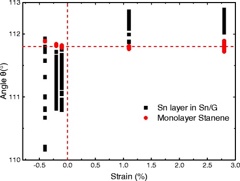
Distribution of the bond angles in Sn layer of different heterostructure models in Table 1 and corresponding monolayer stanene
The vdW interaction between the layers requires special attention. To quantitatively characterize the interlayer interaction strength, we define a binding energy (E b, per Sn atom) in the Sn/G bilayer as
| 2 |
where E Sn/G, E Sn, and E G represent the total energies of the Sn/G heterostructure, corresponding monolayer stanene, and monolayer graphene, respectively, and N Sn is the number of Sn atoms in this structure. This binding energy for the bilayer is evaluated by various exchange-correlation functionals, and the results as a function of the layer separation are shown in Fig. 3. Except for the PBE-GGA that fails to create any binding between the layers, other functionals (LDA and PBE-vdW-DF2) predict energy minima at an interlayer separation around 3.5–3.7 Å. The LDA gives an energy lowering of 72 meV per Sn atom due to the interlayer interaction, which is higher about 70 meV than the case of explicit PBE vdW calculations, suggesting that the results of PBE vdW method are more credible due to the interlayer interaction. Since we are mostly concerned with relative energies and the electronic structure in the present work, and the variation in the interlayer separation around 3.5–3.7 Å is not expected to significantly affect the results. In the following, we will report LDA results at an interlayer separation of 3.5 Å for the simplicity of the calculations. As shown in Table 1 and E b in Fig. 5b, the smallest strain structure has the lowest binding energy, which is −78 meV per Sn atom, corresponding the strongest binding effect. The value is similar to that of graphene/silicene (−66 meV per C atom) within a plane-wave basis set [40]. It indicates that our calculations for E b were reliable. The weak vdW interactions dominate between stanene and graphene, suggesting that graphene can be used as an ideal substrate for stanene. Moreover, to verify the reliability of the equilibrium interlayer distance D, different initial layer distance (2.5–3.9 Å) between stanene and graphene has been fully relaxed, getting up to an identical distance (3.4–3.5 Å) and a uniform buckling height Δ = 0.8 Å as shown in Fig. 4.
Fig. 3.
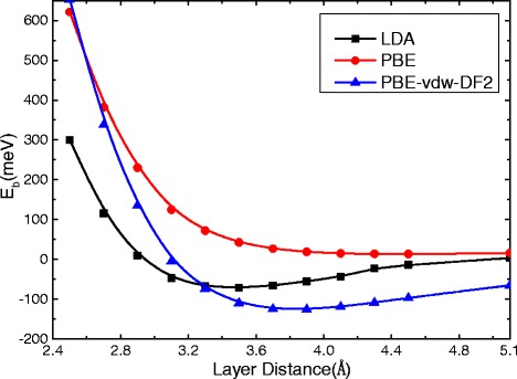
Interlayer binding energy per Sn atom of the bilayer as a function of interlayer spacing. Results using different exchange-correlation functionals are shown. See text for the geometry and the binding energy definition
Fig. 5.
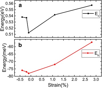
Binding energy (per Sn atom) E b and energy per Sn in comparison with the bulk value E c for stanene on graphene obtained using various supercell models in Table 1. The results (a E c and b E b) are plotted as a function of strain in the layer
Fig. 4.
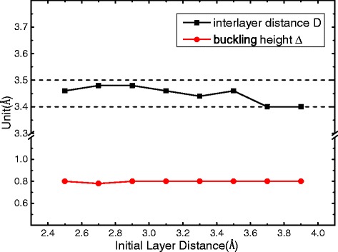
Equilibrium interlayer distance D of the bilayer Sn(7)/G(5) and buckling height Δ of Sn layer obtained from optimized structure of different initial interlayer distance
The energetics of the stanene overlayer can be addressed by examining the energy per Sn atom defined as:
| 3 |
where μ Sn is the chemical potential set to the energy per atom of bulk Sn. The calculated energies per Sn atom using different heterostructures in Table 1 are plotted as a function of the strain in Fig. 5a. The value of E c is positive, indicating that the 2D structure is higher in energy than the 3D diamond structure. Among all the heterostructures we have considered, has the smallest strain (−0.1%) and the lowest energy as expected. The energy difference per atom between different supercell models is smaller than the thermal energy at room temperature (about 26 meV), indicating that multiple phases of different crystalline orientation could coexist at room temperature.
Electronic Structure
Two-dimensional honeycomb structures exhibit a symmetry between the sublattices and therefore have a linear energy dispersion in the vicinity of the Dirac points at K point. Figure 6c shows the projected band structures of . The relative contribution of stanene is coded by color, in which blue (red) corresponds to the state originating only from stanene (graphene). For comparison, the energy band structures of the corresponding graphene and isolated stanene monolayer are also show in Fig. 6a, b. For , the electronic structure is not a simple sum of those of each constituent. Forcing on the position of Dirac point reference to the Fermi level, we found a significant change. The Dirac point of stanene locates at Γ shift 0.1 eV above the Fermi level, while graphene moves 0.2 eV below the Fermi level. Meanwhile, it can be seen that, at the Γ point, the π and π* bands repulse each other, forming a band gap as large as 67 meV. The Fermi level crosses the two Dirac zones of stanene and graphene, inducing weak p-type and n-type doping of them, respectively, and generating a small amount of electron transfer from stanene to graphene. Based on the linear Dirac-like dispersion relation E(k) = ± ℏν F|k| around the Fermi levels [55], the charge carrier (hole or electron) concentration of doped graphene can be estimated by the following equation [56, 57]:
| 4 |
Fig. 6.
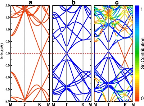
Electronic structures of the a monolayer graphene, b monolayer stanene, and c bilayer . The red line represents the Fermi level, which set to be zero. The relative contribution of stanene is coded by color: blue (red) corresponds to the state originating only from stanene (graphene). The substrate-induced gap is 67 meV for Sn (Γ) and 3 meV for graphene (K)
where ΔE D is the shift of graphene’s Dirac point (E D) relative to the Fermi level (E F), that is ΔE D = E D − E F. Our calculated charge carrier concentrations are N h (Sn) = 1.4 × 1012 cm−2 and N e (G) = 1.6 × 1011 cm−2 for stanene and graphene in bilayer, respectively. These values are larger than the intrinsic charge carrier concentration of graphene at room temperature ( n = πkB 2T2/6ℏνF 2 = 6 × 1010cm− 2) [58]. Furthermore, the charge carrier concentrations of both stanene and graphene in Sn/G heterostructure can be tuned via the interfacial spacing [59]. The self-doping phenomenon in Sn/G heterostructure provides an effective and tunable way for new optoelectronic devices.
Figure 7 shows the band structure of other four supercell models. We can find that the position of the Dirac point located at different high-symmetry point results from the band-folding caused by the various supercell. The graphene substrate introduces an inhomogeneous potential that breaks the sublattice symmetry of stanene. For a free-standing stanene monolayer, the bond angles are uniform. For the graphene-supported layer, the bond angles have a variation, as shown in Fig. 2; hence, the sublattice symmetry is broken, and a gap is opened. And the opened gaps at the Dirac point for , , , , and are 34, 67, 53, 44, and 22 meV, respectively. The spin–orbit coupling effect is also calculated, and the gap at the Dirac point will reduce after adding the SOC. The results suggest that the gap in the bilayer heterostructure could be tuned by the interplay between the substrate and SOC effects, moreover by voltage or strain. The characteristics of the Dirac fermions are preserved as shown in Fig. 7b, c accompanied with a small amount of charge transfer from stanene to graphene, as discussed in .
Fig. 7.
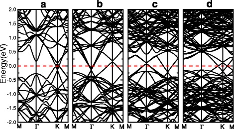
Band structure of a , the Dirac point of them both located at K, b , the Dirac point of stanene (graphene) is located at K (Γ), c , the Dirac point of stanene (graphene) is located at Γ (K), and d , the Dirac points of stanene and graphene are both located at K
When focusing on Fig. 7a, d, we find that the Dirac points of stanene and graphene are located at the same high-symmetry point K. To investigate the mechanisms of action more clearly, the projected band structure and density of states (DOS) of is shown in Fig. 8. It is clearly seen that there exists a band inversion around the Fermi level at K point. For stanene, the original valence band shifts up to the conduction band, while for graphene, the original conduction band turns into valence band which is below the Fermi level. Meanwhile, both the maximum valence band and minimum conduction band are transformed from the “cone shape” to the “Mexican-hat shape,” leading to the appearance of two Dirac feature points with the band gap about 34 meV around the K point. The band inversion associated with the change of band shapes is reminiscent of many topological insulators (TIs) [60, 61]. In order to ascertain the topological phase transition in the heterostructure, we calculate the Z2 topological invariants. We implement the method proposed by Soluyanov and Vanderbilt [62], in which the 2D Z2 invariant is obtained by counting the number of jumps of the “biggest gap” among the 1D hybrid Wannier charge centers [63] (WCCs) during the evolution. Although the results have shown that it exhibits a topologically trivial phase, it would provide a way and useful guideline for the investigation the QSH insulator and the grown of stanene or other 2D vdW heterostructures.
Fig. 8.
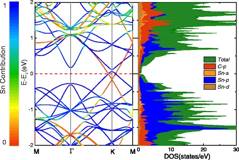
Electronic band structure and DOS of . The relative contribution of stanene is coded by color: blue (red) corresponds to the state originating only from stanene (graphene)
Conclusions
In conclusion, by first-principle calculations, we found it is possible to synthesize stanene on the graphene substrate without destroying its characteristics of the Dirac-fermion-like linear dispersion around Dirac points, due to the weak van der Waals interlayer interaction. In addition, multiple phases of different crystalline orientation of stanene and graphene could coexist at room temperature based on our energetics analysis. Moreover, interlayer interactions in stanene and graphene heterostructure can induce tunable band gaps at stanene’s Dirac point, and weak p-type and n-type doping of stanene and graphene, respectively, generating a small amount of electron transfer from stanene to graphene. For stanene on graphene, the gap created by the substrate effect is of the same order as that induced by the SOC effect. Interestingly, for model , there exists a band inversion around the Dirac zones at K point and emerges a band gap about 34 meV overall the band structure, indicating that it shows a semiconductor feature. Our fundamental study of the structural and electronic properties of these stanene/graphene heterostructures may provide important insight and useful guideline for the grown and applications of stanene or other 2D vdW heterostructures.
Acknowledgements
This work was supported by the National Basic Research Program of China (973 Program) under Grant No. 2014CB643900, the Open Program of State Key Laboratory of Functional Materials for Informatics, the National Natural Science Foundation of China (No. 61675032), the Shanghai Pujiang Program (Grant No. 14PJ1410600), the National Natural Science Foundation for Theoretical Physics Special Fund “Cooperation Program” (No. 11547039), and Shaanxi Institute of Scientific Research Plan projects (No. SLGKYQD2-05).
Authors’ Contributions
LYW carried out the calculations. LYW and PFL wrote the manuscript. JYB, CHY, YXS, and SMW helped in the discussions and analysis of the results. PFL and PFG proposed the initial work, supervised the analysis, and revised the manuscript. All authors read and approved the final manuscript.
Competing Interests
The authors declare that they have no competing interests.
Contributor Information
Pengfei Lu, Email: photon.bupt@gmail.com.
Pengfei Guan, Email: pguan@csrc.ac.cn.
References
- 1.Novoselov KS, Geim AK, Morozov SV, Jiang D, Zhang Y, Dubonos SV, Firsov AA, et al. Electric field effect in atomically thin carbon films. Science. 2004;306:666–669. doi: 10.1126/science.1102896. [DOI] [PubMed] [Google Scholar]
- 2.Geim AK, Novoselov KS. The rise of graphene. Nat Mater. 2007;6:183–191. doi: 10.1038/nmat1849. [DOI] [PubMed] [Google Scholar]
- 3.Zhang S, Zhou J, Wang Q, Chen X, Kawazoe Y, Jena P. Penta-graphene: a new carbon allotrope. Proc Natl Acad Sci. 2015;112(8):2372–2377. doi: 10.1073/pnas.1416591112. [DOI] [PMC free article] [PubMed] [Google Scholar]
- 4.Wang FQ, Yu J, Wang Q, Kawazoe Y, Jena P. Lattice thermal conductivity of penta-graphene. Carbon. 2016;105:424–429. doi: 10.1016/j.carbon.2016.04.054. [DOI] [Google Scholar]
- 5.Li X, Zhang S, Wang FQ, Guo Y, Liu J, Wang Q. Tuning the electronic and mechanical properties of penta-graphene via hydrogenation and fluorination. Phys Chem Chem Phys. 2016;18(21):14191–14197. doi: 10.1039/C6CP01092J. [DOI] [PubMed] [Google Scholar]
- 6.Zhang S, Zhou J, Wang Q, Jena P. Beyond graphitic carbon nitride: nitrogen-rich penta-CN2 sheet. J Phys Chem C. 2016;120(7):3993–3998. doi: 10.1021/acs.jpcc.5b12510. [DOI] [Google Scholar]
- 7.Cahangirov S, Topsakal M, Aktürk E, Şahin H, Ciraci S. Two-and one-dimensional honeycomb structures of silicon and germanium. Phys Rev Lett. 2009;102:236804. doi: 10.1103/PhysRevLett.102.236804. [DOI] [PubMed] [Google Scholar]
- 8.Liu H, Gao J, Zhao J. Silicene on substrates: a way to preserve or tune its electronic properties. J Phys Chem C. 2013;117(20):10353–10359. doi: 10.1021/jp311836m. [DOI] [Google Scholar]
- 9.Gao J, Zhao J. Initial geometries, interaction mechanism and high stability of silicene on Ag (111) surface. Sci Rep. 2012;2:861. doi: 10.1038/srep00861. [DOI] [PMC free article] [PubMed] [Google Scholar]
- 10.Resta A, Leoni T, Barth C, Ranguis A, Becker C, Bruhn T, Le Lay G, et al. Atomic structures of silicene layers grown on Ag (111): scanning tunneling microscopy and noncontact atomic force microscopy observations. Sci Rep. 2013;3:2399. doi: 10.1038/srep02399. [DOI] [PMC free article] [PubMed] [Google Scholar]
- 11.Guo Y, Zhang S, Zhao T, Wang Q. Thermal exfoliation of stoichiometric single-layer silica from the stishovite phase: insight from first-principles calculations. Nanoscale. 2016;8(20):10598–10606. doi: 10.1039/C5NR06788J. [DOI] [PubMed] [Google Scholar]
- 12.Kaloni TP, Singh N, Schwingenschlögl U. Prediction of a quantum anomalous Hall state in Co-decorated silicene. Physical Review B. 2014;89:035409. doi: 10.1103/PhysRevB.89.035409. [DOI] [Google Scholar]
- 13.Ju W, Li T, Su X, Cui H, Li H. Engineering magnetism and electronic properties of silicene by changing adsorption coverage. Appl Surf Sci. 2016;384:65–72. doi: 10.1016/j.apsusc.2016.05.010. [DOI] [Google Scholar]
- 14.Dávila ME, Xian L, Cahangirov S, Rubio A, Le Lay, G (2014). Germanene: a novel two-dimensional germanium allotrope akin to graphene and silicene. New J Phys 16(9):095002
- 15.Li L, Lu SZ, Pan J, Qin Z, Wang YQ, Wang Y, et al. Buckled germanene formation on Pt (111) Adv Mater. 2014;26(28):4820–4824. doi: 10.1002/adma.201400909. [DOI] [PubMed] [Google Scholar]
- 16.Singh N, Schwingenschlögl U. Topological phases of silicene and germanene in an external magnetic field: quantitative results. Physica status solidi (RRL)-Rapid Research Letters. 2014;8(4):353–356. doi: 10.1002/pssr.201409025. [DOI] [Google Scholar]
- 17.Watanabe K, Taniguchi T, Kanda H. Direct-bandgap properties and evidence for ultraviolet lasing of hexagonal boron nitride single crystal. Nat Mater. 2004;3(6):404–409. doi: 10.1038/nmat1134. [DOI] [PubMed] [Google Scholar]
- 18.Song L, Ci L, Lu H, Sorokin PB, Jin C, Ni J, et al. Large scale growth and characterization of atomic hexagonal boron nitride layers. Nano Lett. 2010;10(8):3209–3215. doi: 10.1021/nl1022139. [DOI] [PubMed] [Google Scholar]
- 19.Hong J, Hu Z, Probert M, Li K, Lv D, Yang X et al (2015) Exploring atomic defects in molybdenum disulphide monolayers. Nature communications 6:6293 [DOI] [PMC free article] [PubMed]
- 20.He H, Lu P, Wu L, Zhang C, Song Y, Guan P, Wang S. Structural properties and phase transition of Na adsorption on monolayer MoS2. Nanoscale Res Lett. 2016;11(1):1–8. doi: 10.1186/s11671-015-1209-4. [DOI] [PMC free article] [PubMed] [Google Scholar]
- 21.Cai Y, Chu CP, Wei CM, Chou MY. Stability and electronic properties of two-dimensional silicene and germanene on graphene. Physical Review B. 2013;88(24):245408. doi: 10.1103/PhysRevB.88.245408. [DOI] [Google Scholar]
- 22.Liu B, Baimova JA, Reddy CD, Dmitriev SV, Law WK, Feng XQ, Zhou K. Interface thermal conductance and rectification in hybrid graphene/silicene monolayer. Carbon. 2014;79:236–244. doi: 10.1016/j.carbon.2014.07.064. [DOI] [Google Scholar]
- 23.Roth S, Matsui F, Greber T, Osterwalder J. Chemical vapor deposition and characterization of aligned and incommensurate graphene/hexagonal boron nitride heterostack on Cu (111) Nano Lett. 2013;13(6):2668–2675. doi: 10.1021/nl400815w. [DOI] [PubMed] [Google Scholar]
- 24.Yang W, Chen G, Shi Z, Liu CC, Zhang L, Xie G, et al. Epitaxial growth of single-domain graphene on hexagonal boron nitride. Nat Mater. 2013;12(9):792–797. doi: 10.1038/nmat3695. [DOI] [PubMed] [Google Scholar]
- 25.Kaloni TP, Gangopadhyay S, Singh N, Jones B, Schwingenschlögl U. Electronic properties of Mn-decorated silicene on hexagonal boron nitride. Physical Review B. 2013;88(23):235418. doi: 10.1103/PhysRevB.88.235418. [DOI] [Google Scholar]
- 26.Ding Y, Wang Y. Electronic structures of silicene/GaS heterosheets. Appl Phys Lett. 2013;103(4):043114. doi: 10.1063/1.4816753. [DOI] [Google Scholar]
- 27.Feng JW, Liu YJ, Wang HX, Zhao JX, Cai QH, Wang XZ. Gas adsorption on silicene: a theoretical study. Comput Mater Sci. 2014;87:218–226. doi: 10.1016/j.commatsci.2014.02.025. [DOI] [Google Scholar]
- 28.Roy K, Padmanabhan M, Goswami S, Sai TP, Ramalingam G, Raghavan S, Ghosh A. Graphene-MoS2 hybrid structures for multifunctional photoresponsive memory devices. Nat Nanotechnol. 2013;8(11):826–830. doi: 10.1038/nnano.2013.206. [DOI] [PubMed] [Google Scholar]
- 29.Zhang W, Chuu CP, Huang JK, Chen CH, Tsai ML, Chang YH et al (2014) Ultrahigh-gain photodetectors based on atomically thin graphene-MoS2 heterostructures. Scientific reports 4(7484):3826–3826 [DOI] [PMC free article] [PubMed]
- 30.Bernardi M, Palummo M, Grossman JC. Extraordinary sunlight absorption and one nanometer thick photovoltaics using two-dimensional monolayer materials. Nano Lett. 2013;13(8):3664–3670. doi: 10.1021/nl401544y. [DOI] [PubMed] [Google Scholar]
- 31.Yu Y, Hu S, Su L, Huang L, Liu Y, Jin Z, Purezky AA, Geohegan DB, Kim KW, Zhang Y, Cao L, et al. Equally efficient interlayer exciton relaxation and improved absorption in epitaxial and nonepitaxial MoS2/WS2 heterostructures. Nano Lett. 2014;15(1):486–491. doi: 10.1021/nl5038177. [DOI] [PubMed] [Google Scholar]
- 32.Liu H, Neal AT, Zhu Z, Luo Z, Xu X, Tománek D, Ye PD. Phosphorene: an unexplored 2D semiconductor with a high hole mobility. ACS Nano. 2014;8(4):4033–4041. doi: 10.1021/nn501226z. [DOI] [PubMed] [Google Scholar]
- 33.Padilha JE, Fazzio A, da Silva AJ. van der Waals heterostructure of phosphorene and graphene: tuning the Schottky barrier and doping by electrostatic gating. Phys Rev Lett. 2015;114(6):066803. doi: 10.1103/PhysRevLett.114.066803. [DOI] [PubMed] [Google Scholar]
- 34.Liu CC, Jiang H, Yao Y. Low-energy effective Hamiltonian involving spin-orbit coupling in silicene and two-dimensional germanium and tin. Physical Review B. 2011;84(19):195430. doi: 10.1103/PhysRevB.84.195430. [DOI] [Google Scholar]
- 35.Xu Y, Yan B, Zhang HJ, Wang J, Xu G, Tang P, Zhang SC, et al. Large-gap quantum spin Hall insulators in tin films. Phys Rev Lett. 2013;111(13):136804. doi: 10.1103/PhysRevLett.111.136804. [DOI] [PubMed] [Google Scholar]
- 36.Fang Y, Huang ZQ, Hsu CH, Li X, Xu Y, Zhou Y et al (2015) Quantum spin Hall states in stanene/Ge (111). Scientific reports 5:14196 [DOI] [PMC free article] [PubMed]
- 37.Zhang GF, Li Y, Wu C. Honeycomb lattice with multiorbital structure: topological and quantum anomalous Hall insulators with large gaps. Physical Review B. 2014;90(7):075114. doi: 10.1103/PhysRevB.90.075114. [DOI] [Google Scholar]
- 38.Gao J, Zhang G, Zhang YW. Exploring Ag (111) substrate for epitaxially growing monolayer stanene: a first-principles study. Sci Rep. 2016;6:29107. doi: 10.1038/srep29107. [DOI] [PMC free article] [PubMed] [Google Scholar]
- 39.Zhou H, Cai Y, Zhang G, Zhang YW. Quantum thermal transport in stanene. Physical Review B. 2016;94(4):045423. doi: 10.1103/PhysRevB.94.045423. [DOI] [Google Scholar]
- 40.Zhang RW, Ji WX, Zhang CW, Li P, Wang PJ. Prediction of flatness-driven quantum spin Hall effect in functionalized germanene and stanene. Phys Chem Chem Phys. 2016;18(40):28134–28139. doi: 10.1039/C6CP06216D. [DOI] [PubMed] [Google Scholar]
- 41.Xu Y, Gan Z, Zhang SC. Enhanced thermoelectric performance and anomalous Seebeck effects in topological insulators. Phys Rev Lett. 2014;112(22):226801. doi: 10.1103/PhysRevLett.112.226801. [DOI] [PubMed] [Google Scholar]
- 42.Wang J, Xu Y, Zhang SC. Two-dimensional time-reversal-invariant topological superconductivity in a doped quantum spin-Hall insulator. Physical Review B. 2014;90(5):054503. doi: 10.1103/PhysRevB.90.054503. [DOI] [Google Scholar]
- 43.Wu SC, Shan G, Yan B. Prediction of near-room-temperature quantum anomalous Hall effect on honeycomb materials. Phys Rev Lett. 2014;113(25):256401. doi: 10.1103/PhysRevLett.113.256401. [DOI] [PubMed] [Google Scholar]
- 44.Zhu FF, Chen WJ, Xu Y, Gao CL, Guan DD, Liu CH, Jia JF et al (2015). Epitaxial growth of two-dimensional stanene. Nat Mater 14(10):1020-1025 [DOI] [PubMed]
- 45.Kohn W, Sham LJ. Self-consistent equations including exchange and correlation effects. Phys Rev. 1965;140(4A):A1133. doi: 10.1103/PhysRev.140.A1133. [DOI] [Google Scholar]
- 46.Kresse G, Furthmüller J. Efficiency of ab-initio total energy calculations for metals and semiconductors using a plane-wave basis set. Comput Mater Sci. 1996;6(1):15–50. doi: 10.1016/0927-0256(96)00008-0. [DOI] [Google Scholar]
- 47.Blöchl PE. Projector augmented-wave method. Physical Review B. 1994;50(24):17953. doi: 10.1103/PhysRevB.50.17953. [DOI] [PubMed] [Google Scholar]
- 48.Kresse G, Joubert D. From ultrasoft pseudopotentials to the projector augmented-wave method. Physical Review B. 1999;59(3):1758. doi: 10.1103/PhysRevB.59.1758. [DOI] [Google Scholar]
- 49.Ceperley DM, Alder BJ. Ground state of the electron gas by a stochastic method. Phys Rev Lett. 1980;45(7):566. doi: 10.1103/PhysRevLett.45.566. [DOI] [Google Scholar]
- 50.Perdew JP, Burke K, Ernzerhof M. Generalized gradient approximation made simple. Phys Rev Lett. 1996;77(18):3865. doi: 10.1103/PhysRevLett.77.3865. [DOI] [PubMed] [Google Scholar]
- 51.Grimme S. Semiempirical GGA‐type density functional constructed with a long‐range dispersion correction. J Comput Chem. 2006;27(15):1787–1799. doi: 10.1002/jcc.20495. [DOI] [PubMed] [Google Scholar]
- 52.Monkhorst HJ, Pack JD. Special points for Brillouin-zone integrations. Physical review B. 1976;13(12):5188. doi: 10.1103/PhysRevB.13.5188. [DOI] [Google Scholar]
- 53.Riedl C, Coletti C, Starke U. Structural and electronic properties of epitaxial graphene on SiC (0 0 0 1): a review of growth, characterization, transfer doping and hydrogen intercalation. J Phys D Appl Phys. 2010;43(37):374009. doi: 10.1088/0022-3727/43/37/374009. [DOI] [Google Scholar]
- 54.Wang D, Chen L, Wang X, Cui G, Zhang P. The effect of substrate and external strain on electronic structures of stanene film. Phys Chem Chem Phys. 2015;17(40):26979–26987. doi: 10.1039/C5CP04322K. [DOI] [PubMed] [Google Scholar]
- 55.Neto AC, Guinea F, Peres NM, Novoselov KS, Geim AK. The electronic properties of graphene. Rev Mod Phys. 2009;81(1):109. doi: 10.1103/RevModPhys.81.109. [DOI] [Google Scholar]
- 56.Wang Y, Ni Z, Liu Q, Quhe R, Zheng J, Ye M, et al. All-metallic vertical transistors based on stacked Dirac materials. Adv Funct Mater. 2015;25(1):68–77. doi: 10.1002/adfm.201402904. [DOI] [Google Scholar]
- 57.Qin R, Wang CH, Zhu W, Zhang Y. First-principles calculations of mechanical and electronic properties of silicene under strain. Aip Advances. 2012;2(2):022159. doi: 10.1063/1.4732134. [DOI] [Google Scholar]
- 58.Chen ZY, Santoso I, Wang R, Xie LF, Mao HY, Huang H, et al. Surface transfer hole doping of epitaxial graphene using MoO3 thin film. Appl PhysLett. 2010;96:213104. [Google Scholar]
- 59.Hu W, Yang J. First-principles study of two-dimensional van der Waals heterojunctions. Comput Mater Sci. 2016;112:518–526. doi: 10.1016/j.commatsci.2015.06.033. [DOI] [Google Scholar]
- 60.Du A, Ng YH, Bell NJ, Zhu Z, Amal R, Smith SC. Hybrid graphene/titania nanocomposite: interface charge transfer, hole doping, and sensitization for visible light response. J Phys Chem Letters. 2011;2(8):894–899. doi: 10.1021/jz2002698. [DOI] [PubMed] [Google Scholar]
- 61.Ristein J, Mammadov S, Seyller T. Origin of doping in quasi-free-standing graphene on silicon carbide. Phys Rev Lett. 2012;108(24):246104. doi: 10.1103/PhysRevLett.108.246104. [DOI] [PubMed] [Google Scholar]
- 62.Soluyanov AA, Vanderbilt D. Computing topological invariants without inversion symmetry. Physical Review B. 2011;83(23):235401. doi: 10.1103/PhysRevB.83.235401. [DOI] [Google Scholar]
- 63.Marzari N, Vanderbilt D. Maximally localized generalized Wannier functions for composite energy bands. Physical review B. 1997;56(20):12847. doi: 10.1103/PhysRevB.56.12847. [DOI] [Google Scholar]


