Abstract
Molybdenum disulfide (MoS2) flakes can grow beyond the edge of an underlying substrate into a planar freestanding crystal. When the substrate edge is in the form of an aperture, reagent-limited nucleation followed by edge growth facilitate direct and selective growth of freestanding MoS2 membranes. We have found conditions under which MoS2 grows preferentially across micrometer-scale prefabricated solid-state apertures in silicon nitride membranes, resulting in sealed membranes that are one to a few atomic layers thick. We have investigated the structure and purity of our membranes by a combination of atomic-resolution transmission electron microscopy, elemental analysis, Raman spectroscopy, photoluminescence spectroscopy, and low-noise ion-current recordings through nanopores fabricated in such membranes. Finally, we demonstrate the utility of fabricated ultrathin nanopores in such membranes for single-stranded DNA translocation detection.
Keywords: nanopores, 2D materials, transfer-free, dichalcogenides, MoS2, DNA
Graphical Abstract
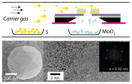
Pioneering studies of exfoliated single-and few-layer graphene and other 2D sheets spawned a new field that explores the physics of two-dimensional materials.1,2 Among this family of 2D materials, molybdenum disulfide (MoS2) is a layered transition metal dichalcogenide in which unsaturated d-electron interactions give rise to unique material properties.3 MoS2 is a semiconductor with a finite band gap, and is composed of covalently bonded S–Mo–S sheets that are bound by weak van der Waals forces. Moreover, the electronic properties of MoS2,2,4,5 which are strongly affected by quantum confinement, can be tuned by controlling its thickness:2,4,6–8 the band gap of MoS2 can be tuned from direct (~1.8 eV)9 to indirect (~1.0 eV)10 by transitioning from its monolayer to its bulk form, respectively. Further, the band gap of MoS2 can be modified by applying strain to the film/membrane.11 This tunable electronic structure has enabled many applications for MoS2 in optoelectronics, for example, ultra-sensitive photodetectors,12,13 photovoltaic cells,14 and photocatalytic/light emitters.15 Additionally, the low energy band gap of MoS2 results in pronounced photoluminescence (PL) in the visible light range.4,6 Recent studies have shown that PL quantum yields for monolayer MoS2 are ~3 orders of magnitude greater than that of multilayer MoS2, due to radiative recombination across the direct band gap, and further, quantum yields of suspended MoS2 are greater than unsuspended MoS2,4 owing to interactions with the substrate material.16
MoS2 has garnered a lot of interest for biosensing applications.17 The effective Young’s modulus of 270 ± 100 GPa18 is comparable to that of steel, allowing free-standing MoS2 membranes to be used as sensors in aqueous environment without being compromised. Recently, nanopores in ultrathin MoS2 membranes have been fabricated and used for single-molecule DNA sensing.19 For these studies, a high-quality chemical vapor deposition (CVD)-grown MoS2 flake is transferred from its growth substrate to an aperture. The results with MoS2 pores are promising because the thickness of a single MoS2 layer (0.8 nm) may be more ideal than that of a graphene layer (~0.3 nm).20–22 Apart from geometry, the chemical, optical, and electrical properties of MoS2 can be leveraged for next-generation, high-resolution DNA sequencing technologies.23 However, manufacturing of freestanding MoS2 membranes faces hurdles that are related to the slow and serial nature of the flake transfer process, during which flake contamination24,25 and compromised mechanical properties reduce the device fabrication throughput and limit its usability.
In this work, we present an approach for growing freestanding high-quality MoS2 membranes directly on apertures in silicon nitride (SiNx) windows. Building on our recent demonstration of a CVD-based transfer-free process for freestanding graphene membrane fabrication,26 we utilize a catalyst-free CVD process here to controllably grow 2D MoS2 crystals on apertures in freestanding SiNx windows. We have identified conditions under which growth is selective toward the aperture, yielding high quality sealed MoS2 membranes across the aperture. Further, we show via ion-current measurements that electron-beam fabricated nanopores in our MoS2 are ultrathin, and that the low noise of the devices is comparable with low-noise silicon nitride nanopore devices. Finally, we demonstrate single-stranded DNA transport through a 2.3 nm diameter nanopore made in a MoS2 membrane that has a nominal thickness between 1 and 2 layers based on ionic conductance models.
RESULTS AND DISCUSSION
Our simple and straightforward notion of aperture-limited fabrication of freestanding MoS2 membranes and a typical fabrication scheme are shown in Figure 1a. The CVD synthesis method used here is a modified version of a recently developed approach by Bilgin et al. that uses MoO2 and S as the two sources in a CVD chamber.27 Two quartz boats, one containing sulfur powder (99.5%, AlfaAesar) and the other MoO2 powder (99%, Sigma-Aldrich) are placed in a 30 mm O.D. quartz furnace, 15 cm apart. A custom-made silicon support is placed atop the Mo-boat, such that a series of SiNx membrane devices can be placed above the boat. Aperture-containing substrate devices were prepared using a previously described procedure:26 A series of 5 × 5 mm2 chips that contain freestanding 30–50 μm2 membranes of 100 nm-thick freestanding SiNx were cleaned using hot piranha solution and dried with a gentle flow of nitrogen (N2) gas. Next, positive electron beam resist was spun onto the membrane side of the chips, and a single 0.5–2 μm-diameter circular hole was (or pattern of holes were) written on each of the membranes using e-beam lithography (Hitachi S-4800, NPGS EBL software). After resist development, the exposed SiNx was reactive ion-etched (Micro-RIE Series 800) using SF6 plasma as the etch reagent. The residual resist was then stripped using acetone bath and hot piranha treatment. The details of the CVD process are as follows: substrate devices are placed on the Si support that is on top of the MoO2 boat, and the temperature of the furnace is ramped to 300 °C at a rate of 30 °C/min under 180 sccm Ar flow and the furnace is held at this temperature for ~15 min, a step that we found necessary for generating high yield crystals. Following this intermediate temperature step, in which MoO2 sublimes to generate nucleation sites for subsequent MoS2 growth, the temperature is ramped to 750 °C at a rate of 3 °C/min under 180 sccm Ar flow such that sulfur gas flows over the aperture, and the furnace is held at that temperature for 30 min.
Figure 1.
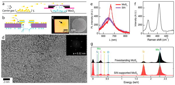
Freestanding MoS2 membranes. (a) Scheme of CVD-based fabrication of MoS2 on aperture-containing silicon nitride (SiNx) membranes (see text for details). (b) Proposed mechanism of aperture-selective growth, in which the CVD growth geometry imposes maximum Mo and S feed concentrations near the aperture. (c) Optical and TEM images of a ~1 μm circular aperture on a SiNx membrane after MoS2 growth. (d) Atomic-resolution image of a freestanding 10 × 20 nm2 MoS2 membrane region. Inset: FFT spectrum of the image. (e) Photoluminescence spectra of a diffraction-limited region ~5 μm away (purple) and within (red) the aperture (excitation wavelength = 532 nm). (f) Raman spectrum of a MoS2 membrane grown on the aperture. (g) Energy dispersive spectra (EDS) of freestanding and SiN-supported MoS2.
We find that the geometry of this CVD scheme results in optimal Mo and S concentrations for selective MoS2 growth near the aperture, as illustrated by the cartoon in Figure 1b. In Figure 1c we show an optical microscope image of a membrane following MoS2 growth (left), as well as a transmission electron micrograph (TEM, JEOL 2010FEG operating in bright-field mode at 200 kV) of a partially covered MoS2 membrane. The TEM image shows two predominant triangular flakes that are suspended over the aperture parallel to the membrane direction. Because typically multiple flakes nucleate over the aperture, there are always regions within the membrane that contain one, two, and more than 2 layers. An aberration-corrected high-resolution transmission electron micrograph (AC-HRTEM, MC Zeiss 80–200 operating at 80 kV) is shown in Figure 1d. The image reveals the high quality of these MoS2 membranes, which exhibit 1 and 2 layer regions that contain virtually no atomic vacancies, minimal contamination, and a monocrystalline nature that is typical of MoS2 (a = 0.32 nm).
The identity of the membranes was characterized using photoluminescence spectroscopy (PL), Raman spectroscopy, and energy dispersive spectroscopy (EDS), as shown in Figure 1e–g, respectively. The PL spectrum, acquired by diffraction-limited confocal illumination of the aperture region using a 532 nm laser illumination and spectrally resolved detection using a 555 nm long-pass emission filter, reveals a sharp peak at λmax = 667 nm that corresponds to MoS2 PL. For comparison, the PL spectrum ~5 μm away from the circle contains strictly the characteristic broadly distributed orange-red SiNx PL. The Raman spectrum collected from the aperture clearly shows MoS2-specific E2g1 and A1g vibrational modes at 379 and 404 cm−1, respectively. Finally, in order to gauge the contamination levels of our grown MoS2 we performed EDS elemental analysis on the freestanding and SiN-supported MoS2 membranes, as shown in Figure 1g (Hitachi HD 2700 Cs-corrected STEM operating at 200 kV, equipped with Bruker EDS system). Both spectra show peaks for Mo (~2.27 keV) and S (~2.30 keV), in addition to Si (~1.73 keV). However, the relative ratios Mo:Si and S:Si are much higher in the freestanding MoS2 area. Observation of Si signal in the freestanding region most likely comes from scattered nearby electrons, since we did not observe any evidence of Si presence in TEM imaging. Finally, carbon contents found in our membranes are much lower than observed with transferred MoS2 membranes,28,29 the presence of carbon being most likely a result of unavoidable contamination during sample handling and/or TEM imaging.
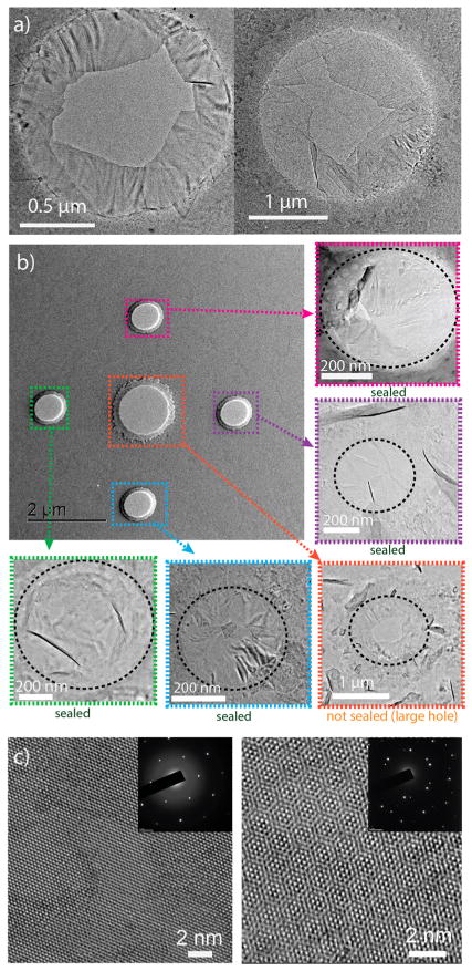
Our approach to CVD MoS2 growth on apertures is kinetically controllable. The TEM images (JEOL 2010FEG operating in bright-field mode at 200 kV) in Figure 2a show partial MoS2 deposition that emanates from a 1.3 μm (left, 30 min growth time) and a 2 μm (right, 60 min growth time) diameter circular aperture. As the images suggest, MoS2 grains first nucleate on the SiNx substrate, and then growth toward the center of the aperture proceeds. By using the growth parameters as indicated above (750 °C, 180 sccm Ar flow), crystal nucleation is slow and full sealing of the aperture with only one to a few layers of MoS2 is obtained. In Figure 2b we show BF-TEM images (JEOL 2010FEG operating in bright-field mode at 200 kV) of five micron-scale apertures (four ~1 μm apertures and a central 1.8 μm aperture, see large image) onto which MoS2 was deposited for the purpose of obtaining complete thin seal. The peripheral images show close-up views of each aperture following the deposition. Apart from the larger aperture, which did not close fully, all of the four 1 μm holes were found to be fully sealed.
Figure 2.
TEM images of MoS2 membranes. (a) Incomplete MoS2 deposition on a 1.3 μm (left) and a 2 μm (right) diameter circular apertures (see text for details), which show that MoS2 grains nucleate from the SiNx substrate inward. (b) Large image: array of 5 apertures prior to MoS2 growth. Following growth, the smaller four apertures (~1 μm each) are fully sealed with one to few layers of MoS2, whereas the larger aperture is not completely sealed. (c) High-resolution TEM images of different regions within the sealed membranes, which show areas of epitaxial and nonepitaxial arrangement of MoS2 layers. Insets: diffraction patterns obtained from regions within the images.
In Figure 2c we show high-resolution TEM images (MC Zeiss 80–200 operating at 80 kV) of two regions within a sealed membrane, as well as respective selected area electron diffraction (SAED) pattern acquired from regions within the images. In the left image only one set of a 6-fold symmetry diffraction spots, confirming epitaxial arrangement of the layer/s (some portions of the image are multilayered, whereas others are single layer). In contrast, the image on the right shows a superhexagonal moiré pattern formation between two nonepitaxial crystalline planes. As the SAED pattern in the inset shows, this moiré pattern is the result of two superimposed grains that are positioned with a relative orientation of ~15° to each other, obtained during independent growth of two adjacent crystals. The only possible interaction between these two grains could be mediated by weak van der Waals forces.
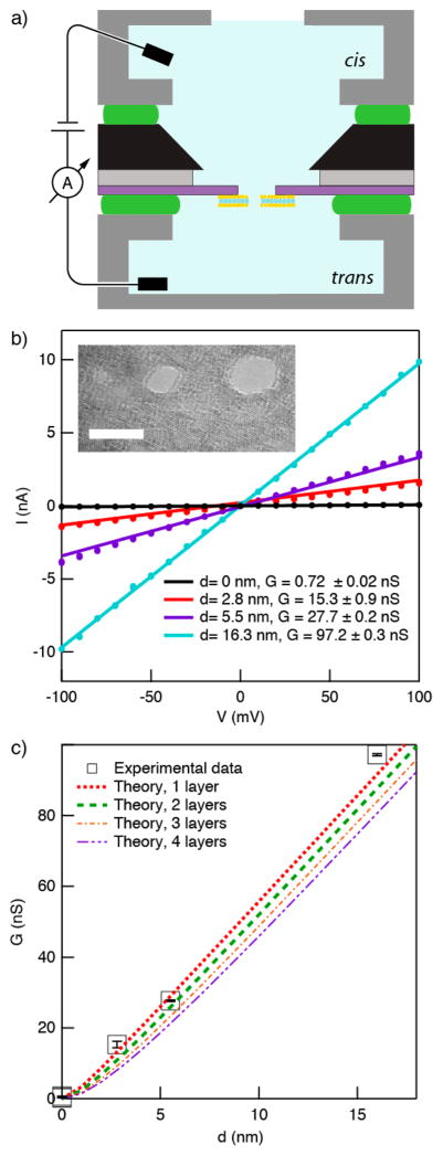
Following our optimization of hole-free membrane growth, we have grown complete MoS2 membranes on several devices and used a TEM beam to fabricate nanopores30 in these membranes in order to study ion transport through these pores. Because of the extremely thin membrane structure, only brief ~1–2 s exposure times to a focused beam were sufficient to produce nanopores, and great care had to be taken (i.e., reduction of spot size, beam current) to avoid large pore formation. Following the fabrication of several pores of different diameters, the chips were assembled into a custom-made PTFE cell as shown in Figure 3a. Prior to measurements, a chip was glued onto the top PTFE portion of the cell using a quick-curing elastomer, and a second layer of glue was applied to the membrane such that only ~1 mm2 was exposed, in order to minimize capacitance-mediated noise.31 After elastomer curing, the cell was assembled, the cis and trans compartments were filled with 0.40 M KCl electrolyte buffered to pH 8.0 using 10 mM Tris (Gbulk = 50 mS/cm), and a pair of Ag/AgCl wire electrodes immersed in the chambers was plugged into a Chimera Instruments high-bandwidth amplifier.32 Figure 3b shows the current–voltage response of the MoS2 membranes with pores of various diameters. While for the membrane without pores we did not measure any appreciable current, for the three nanopores tested we observed linear current/voltage responses that are characteristic of ion-conducting nanopores. Linear fitting of the slopes of the curves yields the membrane conductance (G) values, which are reported in the legend of the figure. The inset TEM image (JEOL 2010FEG operating in bright-field mode at 200 kV) displays several nanopores fabricated using an electron beam adjacent to each other, ranging in diameter from 1 to 5 nm. To rationalize our observed conductance levels for these pore diameters, in Figure 3c we plot the theoretically expected conductance for circular nanopores of ideal diameter d in MoS2 membranes of quantized thicknesses in the range of 1–4 layers (where each layer is 0.8 nm thick). To obtain these curves we must take into account access resistance in ultrathin membranes,33,34 which yields the conductivity G for MoS2
Figure 3.
Ion transport measurements through nanopores in MoS2 membrane devices. (a) Scheme of setup (see text). (b) Current–voltage curves of several nanopores (0.40 M KCl, pH 8, T = 21 °C, pore diameter d and conductance G indicated in legend). Inset shows TEM image of several pores drilled adjacent to each other (scale bar = 5 nm). (c) Comparison of our experimental G and d values with theoretical curves computed for 1–4 MoS2 layers using eq 1.
| (1) |
where σ is the bulk electrolyte conductivity, n is the number of MoS2 layers, h is a monolayer thickness (0.8 nm), and d is the pore diameter. In the figure we also plot the conductance for three MoS2 membranes that contained no fabricated nanopores, in which the mean conductance was 0.43 nS, a factor of 35 smaller than the conductance of the 2.8 nm pore. Overall, our experimental data points to pores that are 1–2 layers thick, apart from a small negative deviation for the larger pore, which most likely stems from ~10% error in pore diameter. In summary, while these data do not directly prove that our pores are of thickness that corresponds to a single MoS2 layer, thin 1–2 layer thick pore structures are highly likely based on the observed conductance values and TEM images.
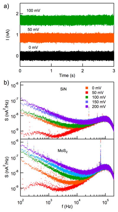
Next, we compared the ion-current noise exhibited by our MoS2 nanopores to that of SiNx pores. In Figure 4a we show 3-s current vs time snapshots for the smallest pore in the series (d = 2.8 nm) at different applied voltages. The traces were acquired using a Chimera Instruments high-bandwidth amplifier,32 which digitally samples the ion current at 4.17 MHz, although the traces shown in the figure have been digitally low-pass filtered at 200 kHz. Remarkably, DC current values were very stable, with peak-to-peak noise values of ~400 pA at 200 kHz. Power spectral density plots shown in Figure 4b for different applied voltages in range 0–200 mV show that the noise is comparable to nanopores in SiNx membranes at this bandwidth.35 Both pores exhibit typical 1/f noise regions that decrease with frequency until overwhelmed by capacitive noise at f > 104 Hz, which is dampened using the 200 kHz digital low-pass filter (shoulders on right). The 1/f noise in our MoS2 membranes is atypical of 2D pores. In comparison, graphene pores, due to their more hydrophobic nature and charge fluctuations in the material, display larger 1/f current noise values than MoS2 or than their ceramic counterparts (e.g., SiNx, HfO2). Heerema and co-workers,36 as well as Merchant and co-workers,37 reported for a transferred graphene pore noise density of ~10−4 nA2/Hz at a frequency of 100 Hz, whereas Waduge found for transfer-free graphene pore a noise value of ~10−5 nA2/Hz at 200 mV. In contrast, for MoS2 and SiN pores of similar conductance values and voltages we observe noise densities at 100 Hz below 10−6 and ~10−7 nA2/Hz, respectively. This value for MoS2 is lower than the noise reported by Feng and co-workers for a transferred MoS2 pore.38 Recently, 1/f noise in graphene has been attributed to mechanical fluctuations in the thin material.36 Since we have recently observed lower noise levels in transfer-free graphene than in transferred graphene, we conclude that the even lower noise exhibited by our polycrystalline MoS2 membrane directly grown on apertures is likely a combination of superior mechanical stability afforded by the direct growth and a material-specific low noise of MoS2.
Figure 4.
Ion-current noise in MoS2 pores. (a) Current vs time traces of a d = 2.8 nm MoS2 pore at different voltages (data low-pass filtered at 200 kHz). (b) Power spectral density plots at different voltages for a d = 4.7 nm SiN pore (G = 14 nS) and a d = 2.8 nm MoS2 pore with similar conductance (G = 15 nS).
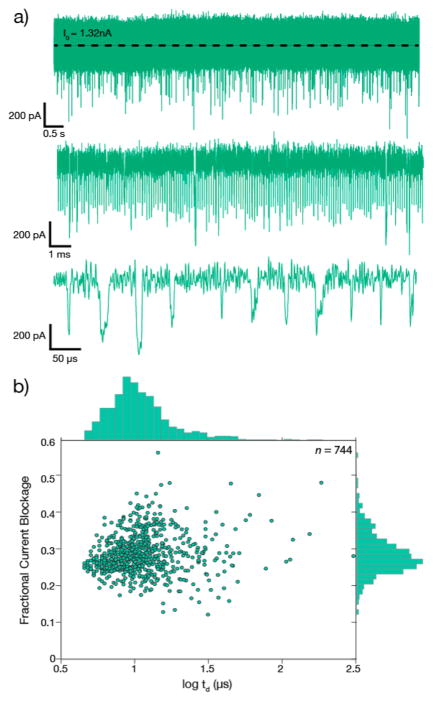
Finally, we have tested the utility of MoS2 nanopores in DNA transport experiments by studying the transport of single-stranded DNA (ssDNA) through a MoS2 pore. Rather than using TEM fabrication, for this study we have used the recently described electrochemical reaction (ECR) process.38 Briefly, we applied a voltage of 1 V for 10–15 s, after which we observed a jump in the membrane conductance and the voltage was turned off. After measuring a pore conductance of ~5 nS, 153-mer ssDNA sample was added to a total concentration of 20 nM, a 200 mV voltage was applied, and current traces were recorded. In Figure 5a we show a sample 3-s current trace, which displays a stochastic set of downward current pulses, each indicating the transport of individual DNA molecules through the pore. Below the continuous current trace in Figure 5a we show concatenated sets of events that were analyzed using Pythion software. In Figure 5b we show a scatter plot of the fractional current blockade (defined as the ratio of the spike mean amplitude to the open pore current) vs dwell time for the 744 events in the experiment. Because of our 200 kHz bandwidth, events below 3 μs are significantly distorted and therefore were discarded from the analysis. Histograms of both parameters are also shown above and to the right of the scatter plots, from which we extract mean dwell times of 16 μs and mean fractional current blockades of 26%. On the basis of the values of the open pore current (1.32 nA at 200 mV) and the mean blockade values, we estimated an effective pore diameter and thickness of 2.3 nm and two MoS2 layers (1.6 nm), respectively.34 Given the relatively large pore size as compared with the nominal diameter of ssDNA (~1.3 nm), mean transport velocities of 0.1 μs/bp are reasonable and in accordance with a prior study.39 Finally, the data in the figure shows many events with dwell times (td) below 10 μs, which makes their detection challenging. However, because the mean capture rate was 0.95 s−1 nM−1 in our experiment, and a mean capture rate of 0.02 s−1 nM−1 was obtained for a 1.7 nm diameter HfO2 pore under similar conditions,40 we reason that DNA capture is efficient in a MoS2 pore.
Figure 5.
Single-stranded DNA transport through a 2.3 nm diameter MoS2 nanopore. (a) Three-second continuous current trace for a 2.3 nm diameter pore after the addition of 20 nM 153-mer ssDNA to the cis chamber ([KCl] = 0.40 M, Vtrans = 200 mV, sampling rate =4.17 MHz, data low-pass filtered to 200 kHz). Concatenated sets of events at different magnifications are shown below the trace. (b) Scatter plot of fractional current blockade (see text) vs dwell time td, as well as histograms of each parameter shown in each corresponding axis (n = number of molecules detected).
CONCLUSIONS
In conclusion, we have developed here a method for CVD-based fabrication of freestanding, insulating, and low-noise MoS2 membranes on solid-state apertures. Flowing sulfur vapor over a microscale aperture that is placed above subliming molybdenum dioxide in a CVD apparatus at atmospheric pressure seals the aperture with high quality one to a few layers of polycrystalline MoS2. Optimization of the CVD growth conditions included adjustment of the growth temperature, cooling/heating rates, growth time, geometry of the feed samples, and carrier gas flow rates. Selective growth near the apertures favors a mechanism in which nucleation and growth are restricted to near the aperture by the geometry of the setup, in which the aperture is exposed to optimal concentrations of both Mo and S vapors. Our investigation of the membrane quality using atomic-resolution transmission electron microscopy, elemental analysis, Raman spectroscopy, photoluminescence spectroscopy, and low-noise ion-current recordings through nanopores fabricated in these membranes, points to a high-quality crystalline membrane with low noise and a good mechanical stability. Finally, we have demonstrated DNA transport measurements through a 2.3 nm diameter pore fabricated using a recently developed method. Although a more detailed study of DNA transport is required, the initial results presented here demonstrate the viability of directly grown MoS2 pores for DNA studies.
Apart from applications in biomolecular analysis, there is vast interest in such membranes for ion filtration and other membrane applications. An attractive feature of our direct-growth technology includes its scalability to wafer-scale quantities. As compared with the painstaking 2D material transfer method to apertures, which requires larger quantities of MoS2, special equipment for transfer, and is associated with low yield of sealed devices, our direct growth method yields favorable quality, low-noise, and a superior scalability.
METHODS
Substrates for MoS2 growth were 5 × 5 mm2 Si chips with a 100 nm-thick SiNx film deposited on a 2.5-μm-thick thermal SiO2 layer to reduce electrical noise. 950 PMMA etch mask was spun onto SiNx and a small region (2 × 2 μm2) was exposed using Nabity NPGS e-beam writing software on a Hitachi S-4800 scanning electron microscope. Exposed PMMA was developed with 3:1 isopropyl alcohol:methyl isobutylketone, and SiNx was etched in a Technics Micro-RIE Series 800 etcher using sulfur hexafluoride (SF6) at 300 mTorr and 150 W. PMMA was then stripped off by 45 min acetone bath and 15 min hot piranha treatment followed by warm water rinse. MoS2 membranes were deposited on SiN windows with apertures using ambient pressure CVD technique in a split tube furnace with 35 mm O.D. quartz tube. The details of the growth procedure are as follows: Two quartz boats, one containing sulfur powder (99.5%, AlfaAesar) and the other MoO2 powder (99%, Sigma-Aldrich) are placed in the furnace 15 cm apart such that the boat containing the S powder is at the upstream of the tube. A custom-made silicon support is placed atop the Mo-boat, such that a series of SiNx membrane devices can be placed above the boat. The temperature of the furnace is ramped to 300 °C at a rate of 30 °C/min under 180 sccm Ar flow and the furnace is held at this temperature for ~15 min. Then the temperature of the furnace is further increased to 750 °C at a rate of 3 °C/min under 180 sccm Ar flow and the furnace is held at that temperature for 30 min. Following the MoS2 growth, the furnace was allowed to naturally cool down to room temperature under 180 sccm Ar flow while the hood of the furnace being opened.
The SiNx chips with MoS2 freestanding membranes were glued in a custom-made PTFE cell using quick-curing elastomer. Both chambers (cis and trans) of the cell were filled with 0.4 M KCl buffer solution (pH 8.0, 10 mM Tris, 1 mM EDTA) and Ag/AgCl electrodes were immersed in each chamber. Before collecting current data, both cis and trans chambers were rinsed several times with 1:1 methanol:buffer solution mixture, and then the washsolution was replaced with aqueous buffer. Ionic current data were collected at sample rate of 4 MS/s and digitally low-passed filtered using a Chimera Instrument VC100 amplifier system. ssDNA was then added to the cis chamber and thoroughly mixed with the buffer to a ~20 nM final concentration. DNA translocation data were analyzed offline using Pythion software, developed at the Wanunu lab (www.github.com/rhenley/Pythion).
Acknowledgments
We acknowledge Fangze Liu and Anthony Vargas for assistance with CVD, and Wentao Liang for assistance with TEM. We also acknowledge the Center for Nanoscale Systems (CNS), a part of Harvard University, for their electron microscopy facilities. Financial support is acknowledged from National Institutes of Health R21-HG006873 (PW, JL, RYH, and MW) and from the National Science Foundation ECCS-1351424 (SK and IB).
Footnotes
Conflict of Interest: The authors declare no competing financial interest.
REFERENCES AND NOTES
- 1.Novoselov KS, Jiang D, Schedin F, Booth TJ, Khotkevich VV, Morozov SV, Geim AK. Two-Dimensional Atomic Crystals. Proc Natl Acad Sci U S A. 2005;102:10451–3. doi: 10.1073/pnas.0502848102. [DOI] [PMC free article] [PubMed] [Google Scholar]
- 2.Radisavljevic B, Radenovic A, Brivio J, Giacometti V, Kis A. Single-Layer MoS2 Transistors. Nat Nanotechnol. 2011;6:147–50. doi: 10.1038/nnano.2010.279. [DOI] [PubMed] [Google Scholar]
- 3.Ganatra R, Zhang Q. Few-Layer MoS2: A Promising Layered Semiconductor. ACS Nano. 2014;8:4074–99. doi: 10.1021/nn405938z. [DOI] [PubMed] [Google Scholar]
- 4.Mak KF, Lee C, Hone J, Shan J, Heinz TF. Atomically Thin MoS2: A New Direct-Gap Semiconductor. Phys Rev Lett. 2010;105:136805. doi: 10.1103/PhysRevLett.105.136805. [DOI] [PubMed] [Google Scholar]
- 5.Eda G, Yamaguchi H, Voiry D, Fujita T, Chen M, Chhowalla M. Photoluminescence from Chemically Exfoliated MoS2. Nano Lett. 2011;11:5111–6. doi: 10.1021/nl201874w. [DOI] [PubMed] [Google Scholar]
- 6.Splendiani A, Sun L, Zhang Y, Li T, Kim J, Chim CY, Galli G, Wang F. Emerging Photoluminescence in Monolayer MoS2. Nano Lett. 2010;10:1271–5. doi: 10.1021/nl903868w. [DOI] [PubMed] [Google Scholar]
- 7.Kuc A, Zibouche N, Heine T. Influence of Quantum Confinement on the Electronic Structure of the Transition Metal Sulfide TS 2. Phys Rev B: Condens Matter Mater Phys. 2011;83:245213. [Google Scholar]
- 8.Liu Y, Nan H, Wu X, Pan W, Wang W, Bai J, Zhao W, Sun L, Wang X, Ni Z. Layer-by-Layer Thinning of MoS2 by Plasma. ACS Nano. 2013;7:4202–9. doi: 10.1021/nn400644t. [DOI] [PubMed] [Google Scholar]
- 9.Ho W, Yu JC, Lin J, Yu J, Li P. Preparation and Photocatalytic Behavior of MoS2 and WS2 Nanocluster Sensitized TiO2. Langmuir. 2004;20:5865–5869. [PubMed] [Google Scholar]
- 10.Gourmelon E, Lignier O, Hadouda H, Couturier G, Bernede J, Tedd J, Pouzet J, Salardenne J. MS2 (M= W, Mo) Photosensitive Thin Films for Solar Cells. Sol Energy Mater Sol Cells. 1997;46:115–121. [Google Scholar]
- 11.Castellanos-Gomez A, Roldan R, Cappelluti E, Buscema M, Guinea F, van der Zant HS, Steele GA. Local Strain Engineering in Atomically Thin MoS2. Nano Lett. 2013;13:5361–6. doi: 10.1021/nl402875m. [DOI] [PubMed] [Google Scholar]
- 12.Yin Z, Li H, Li H, Jiang L, Shi Y, Sun Y, Lu G, Zhang Q, Chen X, Zhang H. Single-Layer MoS2 Phototransistors. ACS Nano. 2012;6:74–80. doi: 10.1021/nn2024557. [DOI] [PubMed] [Google Scholar]
- 13.Lee YH, Zhang XQ, Zhang W, Chang MT, Lin CT, Chang KD, Yu YC, Wang JTW, Chang CS, Li LJ, et al. Synthesis of Large-Area MoS2 Atomic Layers with Chemical Vapor Deposition. Adv Mater. 2012;24:2320–5. doi: 10.1002/adma.201104798. [DOI] [PubMed] [Google Scholar]
- 14.Lopez-Sanchez O, Lembke D, Kayci M, Radenovic A, Kis A. Ultrasensitive Photodetectors Based on Monolayer MoS2. Nat Nanotechnol. 2013;8:497–501. doi: 10.1038/nnano.2013.100. [DOI] [PubMed] [Google Scholar]
- 15.Carladous A, Coratger R, Ajustron F, Seine G, Péchou R, Beauvillain J. Light Emission from Spectral Analysis of Au/MoS2 Nanocontacts Stimulated by Scanning Tunneling Microscopy. Phys Rev B: Condens Matter Mater Phys. 2002;66:045401. [Google Scholar]
- 16.Sercombe D, Schwarz S, Del Pozo-Zamudio O, Liu F, Robinson BJ, Chekhovich EA, Tartakovskii II, Kolosov O, Tartakovskii AI. Optical Investigation of the Natural Electron Doping in Thin MoS2 Films Deposited on Dielectric Substrates. Sci Rep. 2013;3:3489. doi: 10.1038/srep03489. [DOI] [PMC free article] [PubMed] [Google Scholar]
- 17.Sarkar D, Liu W, Xie XJ, Anselmo AC, Mitragotri S, Banerjee K. MoS2 Field-Effect Transistor for Next-Generation Label-Free Biosensors. ACS Nano. 2014;8:3992–4003. doi: 10.1021/nn5009148. [DOI] [PubMed] [Google Scholar]
- 18.Bertolazzi S, Brivio J, Kis A. Stretching and Breaking of Ultrathin MoS2. ACS Nano. 2011;5:9703–9. doi: 10.1021/nn203879f. [DOI] [PubMed] [Google Scholar]
- 19.Liu K, Feng J, Kis A, Radenovic A. Atomically Thin Molybdenum Disulfide Nanopores With High Sensitivity for DNA Translocation. ACS Nano. 2014;8:2504–11. doi: 10.1021/nn406102h. [DOI] [PubMed] [Google Scholar]
- 20.Wells DB, Belkin M, Comer J, Aksimentiev A. Assessing Graphene Nanopores for Sequencing DNA. Nano Lett. 2012;12:4117–4123. doi: 10.1021/nl301655d. [DOI] [PMC free article] [PubMed] [Google Scholar]
- 21.Li J, Zhang Y, Yang J, Bi K, Ni Z, Li D, Chen Y. Molecular Dynamics Study of DNA Translocation through Graphene Nanopores. Phys Rev E. 2013;87:062707. doi: 10.1103/PhysRevE.87.062707. [DOI] [PubMed] [Google Scholar]
- 22.Lv W, Chen M, Wu R. The Impact of the Number of Layers of a Graphene Nanopore on DNA Translocation. Soft Matter. 2013;9:960–966. [Google Scholar]
- 23.Farimani AB, Min K, Aluru NR. DNA Base Detection using a Single-Layer MoS2. ACS Nano. 2014;8:7914–22. doi: 10.1021/nn5029295. [DOI] [PubMed] [Google Scholar]
- 24.Dan Y, Lu Y, Kybert NJ, Luo Z, Johnson ATC. Intrinsic Response of Graphene Vapor Sensors. Nano Lett. 2009;9:1472–1475. doi: 10.1021/nl8033637. [DOI] [PubMed] [Google Scholar]
- 25.Castellanos-Gomez A, Buscema M, Molenaar R, Singh V, Janssen L, Zant HSJvd, Steele GA. Deterministic Transfer of Two-Dimensional Materials by All-Dry Viscoelastic Stamping. 2D Mater. 2014;1:011002. [Google Scholar]
- 26.Waduge P, Larkin J, Upmanyu M, Kar S, Wanunu M. Programmed Synthesis of Freestanding Graphene Nanomembrane Arrays. Small. 2015;11:597–603. doi: 10.1002/smll.201402230. [DOI] [PMC free article] [PubMed] [Google Scholar]
- 27.Bilgin I, Liu F, Vargas A, Winchester A, Man MKL, Upmanyu M, Dani K, Gupta G, Talapatra S, Mohite AD, et al. Chemical Vapor Deposition Synthesized Atomically-Thin Molybdenum Disulfide with Optoelectronic-Grade Crystalline Quality. arXiv.org. e-Print Arch., Condens. Matter. 2015 doi: 10.1021/acsnano.5b02019. arXiv:1504.04888. [DOI] [PubMed] [Google Scholar]
- 28.Van Thanh D, Pan CC, Chu CW, Wei KH. Production of Few-Layer MoS2 Nanosheets through Exfoliation of Lquid N2–Quenched Bulk MoS2. RSC Adv. 2014;4:15586–15589. [Google Scholar]
- 29.Feng H, Hu Z, Liu X. Facile and Efficient Exfoliation of Inorganic Layered Materials using Liquid Alkali Metal Alloys. Chem Commun. 2015;51:10961. doi: 10.1039/c5cc02625c. [DOI] [PubMed] [Google Scholar]
- 30.Storm AJ, Chen JH, Ling XS, Zandbergen HW, Dekker C. Fabrication of Solid-State Nanopores with Single-Nanometre Precision. Nat Mater. 2003;2:537–540. doi: 10.1038/nmat941. [DOI] [PubMed] [Google Scholar]
- 31.Tabard-Cossa V, Trivedi D, Wiggin M, Jetha NN, Marziali A. Noise Analysis and Reduction in Solid-State Nanopores. Nanotechnology. 2007;18:305505. [Google Scholar]
- 32.Rosenstein JK, Wanunu M, Merchant CA, Drndic M, Shepard KL. Integrated Nanopore Sensing Platform with Sub-Microsecond Temporal Resolution. Nat Methods. 2012;9:487–492. doi: 10.1038/nmeth.1932. [DOI] [PMC free article] [PubMed] [Google Scholar]
- 33.Hall JE. Access Resistance of a Small Circular Pore. J Gen Physiol. 1975;66:531–532. doi: 10.1085/jgp.66.4.531. [DOI] [PMC free article] [PubMed] [Google Scholar]
- 34.Wanunu M, Dadosh T, Ray V, Jin JM, McReynolds L, Drndic M. Rapid Electronic Detection of Probe-Specific microRNAs using Thin Nanopore Sensors. Nat Nanotechnol. 2010;5:807–814. doi: 10.1038/nnano.2010.202. [DOI] [PubMed] [Google Scholar]
- 35.Carson S, Wilson J, Aksimentiev A, Wanunu M. Smooth DNA Transport through a Narrowed Pore Geometry. Biophys J. 2014;107:2381–2393. doi: 10.1016/j.bpj.2014.10.017. [DOI] [PMC free article] [PubMed] [Google Scholar]
- 36.Heerema SJ, Schneider GF, Rozemuller M, Vicarelli L, Zandbergen HW, Dekker C. 1/f Noise in Graphene Nanopores. Nanotechnology. 2015;26:074001. doi: 10.1088/0957-4484/26/7/074001. [DOI] [PubMed] [Google Scholar]
- 37.Merchant CA, Healy K, Wanunu M, Ray V, Peterman N, Bartel J, Fischbein MD, Venta K, Luo Z, Johnson ATC, et al. DNA Translocation through Graphene Nanopores. Nano Lett. 2010;10:2915–21. doi: 10.1021/nl101046t. [DOI] [PubMed] [Google Scholar]
- 38.Feng J, Liu K, Graf M, Lihter M, Bulushev RD, Dumcenco D, Alexander DTL, Krasnozhon D, Vuletic T, Kis A, et al. Electrochemical Reaction in Single Layer MoS2: Nanopores Opened Atom by Atom. Nano Lett. 2015;15:3431–8. doi: 10.1021/acs.nanolett.5b00768. [DOI] [PubMed] [Google Scholar]
- 39.McNally B, Wanunu M, Meller A. Electromechanical Unzipping of Individual DNA Molecules using Synthetic Sub-2 nm Pores. Nano Lett. 2008;8:3418–3422. doi: 10.1021/nl802218f. [DOI] [PMC free article] [PubMed] [Google Scholar]
- 40.Larkin J, Henley R, Bell DC, Cohen-Karni T, Rosenstein JK, Wanunu M. Slow DNA Transport through Nanopores in Hafnium Oxide Membranes. ACS Nano. 2013;7:10121–10128. doi: 10.1021/nn404326f. [DOI] [PMC free article] [PubMed] [Google Scholar]


