Abstract
We present the first detailed experimental observation and analysis of nanoparticle electrophoresis through a nanochannel obtained with synchronous high-bandwidth electrical and camera recordings. Optically determined particle diffusion coefficients agree with values extracted from fitting electrical transport measurements to distributions from 1D Fokker–Planck diffusion-drift theory. This combined tracking strategy enables optical recognition and electrical characterization of nanoparticles in solution, which can have a broad range of applications in biology and materials science.
Keywords: Single particle tracking, resistive pulse sensing, polymeric nanochannels, translocation dynamics, nanoparticle diffusion
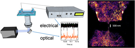
Graphical Abstract
The increasing use of nanomaterials in biomedicine, materials science, foods, and cosmetics calls for the development of new tools and low-cost devices that can identify, manipulate, and characterize nanosized objects.1 Traditional techniques for recognizing and quantifying submicrometer objects, such as electron microscopy, small-angle X-ray scattering, and dynamic light scattering, despite widespread use, suffer several drawbacks: electron microscopy is low-throughput, time-consuming, and costly, while scattering-based techniques provide only ensemble measurements of an average particle size distribution, typically heavily biased toward larger particle sizes.1 Recently, single molecule techniques have emerged including fluorescence correlation spectroscopy (FCS), particle tracking analysis (PTA), and tunable resistive pulse sensing (tRPS). While FCS can accurately probe individual particles, labeling of the sample with a fluorescent dye is required. In contrast, tRPS devices allow label-free detection in the form of electrical spikes that correspond to a rapid change in ion flux caused by a particle occluding a small hole. Despite adaptability to a wide range of particle sizes and applications,2,3 tRPS does not allow direct observation of particles, a feature offered by PTA. This technique is based on recording the light scattered by a single nano-object to reconstruct its trajectory and infer its size analyzing its Brownian motion. While the use of PTA is rapidly spreading4 and commercial instruments are available, the information they provide is significantly poorer than systems combining optical and electrical recordings. In fact, multimodal characterization is rapidly emerging as a valuable strategy for processing complex samples, e.g., for gaining information about both the size and type of a particle in a suspension. In 2013, Yukimoto et al.5 showed that applying optical and electrical sensing to planar microstructured conduits enables unambiguous identification of single-particle translocations. However, the temporal and spatial resolution of their optical data was inadequate to resolve the kinetics of 1.2 µm fluorescent particles crossing the microchannel. More recently, combined optical and electrical detection modalities6 have been applied to nanopore-gated optofluidic devices7 to discriminate among particles of equal size and different optical properties. Solid-state nanopores have also been used for simultaneous electrical and optical detection of DNA,8–11 although direct visualization of particles before, during, and after translocation was not possible in these measurements because of the vertical pore geometry. An easy and inexpensive route to observe the entire process is to use planar nanofluidic devices. In these systems the nanochannel, which is exploited for resistive pulse sensing (RPS), can be directly observed with high resolution objectives, so that RPS can be combined with PTA for a high resolution method of electro-optical nanoparticle tracking (EONT). While electrical signals produced by nanoparticles as they translocate across pores and channels are reasonably well-understood,12,13 little to no information is available from RPS detection before capture and after release. In this work, we analyze the entire translocation process, using electrical signals to size nanoparticles and analyze their motion inside the nanochannel and real-time optical tracking to study their motion in the access regions. This detailed observation of electrophoresis of individual nanoparticles was made possible by the use of planar polymer-based nanofluidic devices, which enabled optical tracking of the entire process.
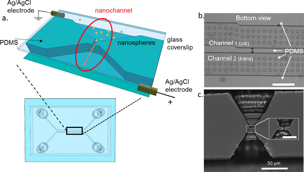
The device used for EONT experiments, schematically shown in Figure 1a, consists of two parallel polydimethylsiloxane (PDMS) microfluidic channels linked by a short submicrometer nanochannel having a triangular section. They are sealed on the bottom via a glass coverslip, which offers the possibility of fluorescence imaging using a high numerical aperture objective. The inset schematically shows the functional part of the device with the nanochannel highlighted by a red oval. As in RPS, an electric field, applied using Ag/AgCl electrodes, electrophoretically drives through the nanochannel charged fluorescent nanoparticles in an electrolytic solution while an ionic current is measured. Resistive pulses produced when nanoparticles cross the nanochannel are recorded electrically, while optical tracking is achieved using high-speed fluorescence imaging.
Figure 1.
(a) Schematic representation of the PDMS nanochannel device sealed onto a glass coverslip. Two microchannels are linked by a nanochannel which is represented in detail in b and c. Ag/AgCl electrodes are placed in opposite reservoirs in order to apply a voltage across the nanochannel (see red oval) to move fluorescent nanospheres through it. (b) Low magnification bright field optical image of the PDMS device in the region with the excavations and the nanochannel, the dots are the pillars that are disseminated along the microchannel to avoid collapse (scale bar 500 µm). (c) Higher magnification image of the area around the nanochannel, obtained after bonding with a glass coverslip (inset scale bar 5 µm).
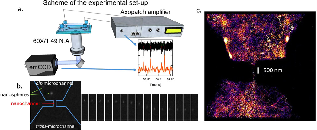
Our sample is a suspension of negatively charged fluorescent nanospheres with a nominal diameter of 40 nm (see SI). Using previously published procedures,14,15 we constructed a planar triangular PDMS nanochannel that is <250 nm in width and height. The sample was placed in the cis chamber and a positive voltage was applied to the trans chamber in order to drive the particles through the nanochannel. Translocations are marked by a stochastic set of ion current reduction spikes. In order to track the nanospheres, we synchronously acquired fluorescence images (1328 frames per second) from a subregion that surrounds the nanochannel. Figure 2a shows a scheme of the setup, as well as a snapshot of the synchronous electrical (black) and optical (red) traces.
Figure 2.
(a) Scheme of the setup, as well as a snapshot of the synchronous electrical (black) and optical (red) traces. (b) A time-lapse series of a particle as it transits the nanochannel (equal time intervals between successive frames). (c) An integrated super-resolution image of an ensemble of particles as these traverse the nanochannel (see SI for details).
A time-lapse series of a particle as it transits the nanochannel (equal time intervals between successive frames) is shown in Figure 2b. From this sequence, it is clear that the particle accelerates as it reaches the center of the nanochannel, which can be explained by the high electric field generated at the channel. We study here the dynamics of nanosphere transport using single particle tracking and electrical measurements. Specifically, we compare here for the first time diffusion coefficients of the particles outside and inside the channel by analyzing optical tracks with Brownian theory and relating the results to theoretical–transport times obtained from electrical measurements using established 1D Fokker–Planck diffusion-drift models.
An integrated super-resolution image of an ensemble of particles as these traverse the nanochannel is shown in Figure 2c (see SI for details). The cross-section of the nanochannel has been designed to have a narrow region in the center, whose width and length have been determined to be 230 ± 50 nm and 500 ± 50 nm, respectively. We observe a dark region in this central constriction due to high particle velocity in the area.
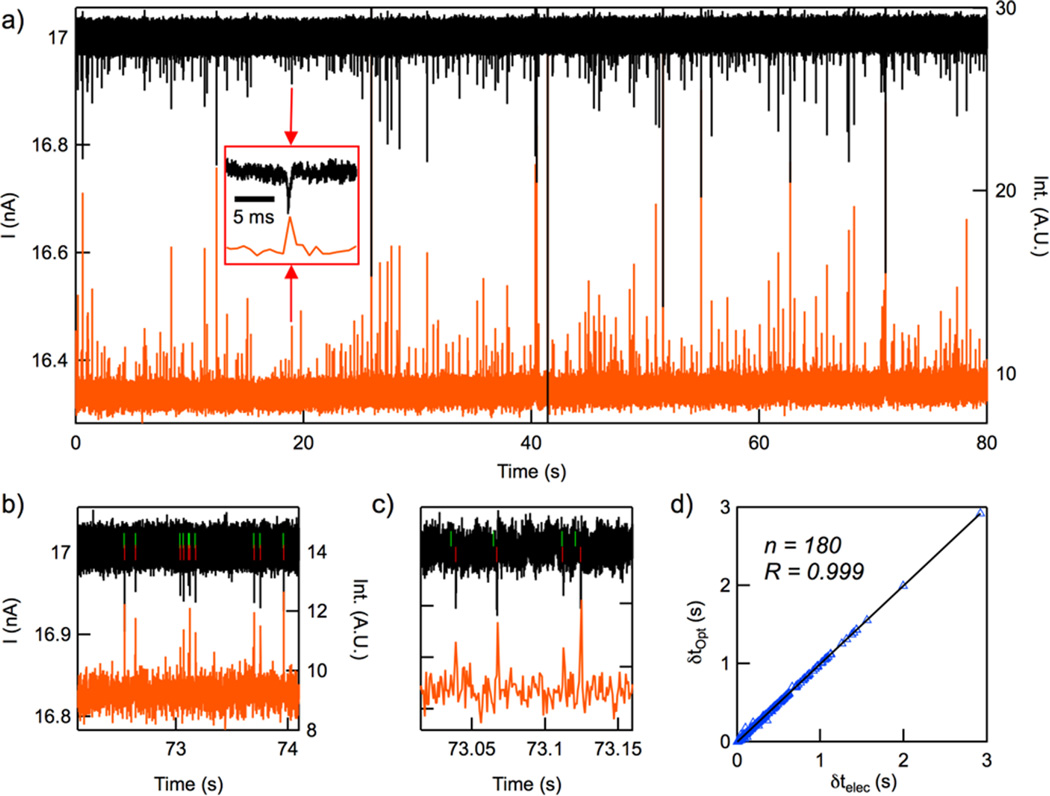
In Figure 3a we show 80 s example electrical (top, black) and optical (bottom, red) nanospheres time traces (V = −350 mV). The translocation of a nanosphere produces negative electrical spikes (increase in channel resistance) and positive fluorescence spikes (increased fluorescence). Close-up views of the traces, shown in Figure 3b–c, highlight an agreement between the two signals in time. Overlaid on the electrical signal are green and red vertical lines that correspond to software-determined electrical and optical event onset, respectively. While the electrical signals preceded the optical signal by as much as 1 ms, as seen in Figure 3c, this time delay δt is on the order of the electrical acquisition rate and therefore may be an artifact of aliasing. For the most part, we see an excellent time correlation R between the two signals, as shown in Figure 3d for a series of 180 spikes extracted from an 80 s trace.
Figure 3.
(a–c) Traces of electrical (black) and optical (red) signals registered during the passage of fluorescent nanospheres through the nanochannel (Vapplied = −350 mV). The green and red ticks are associated with electrical and optical event beginning, respectively. (d) Correlation analysis of the delay time between successive optical δtOpt and electrical δtelec spikes.
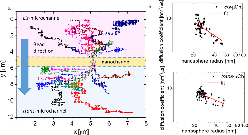
In Figure 4a we show a set of sample trajectories that track the position of individual nanoparticles during their transport through the channel at a voltage of 300 mV. The (x,y) coordinates of the trajectories are extracted from the movies and analyzed to determine the diffusion coefficient outside the nanochannel using Brownian diffusion theory (see SI). As 94% of the voltage drops across the nanochannel at its inlet and outlet, the motion of nanoparticles moving in the cis- and trans-microchannels is analyzed as unbiased diffusion. In order to account for possible differences in D in the cis- and trans-microchannels, i.e., while nanospheres approach and exit the nanochannel, D is estimated for each particle separately in the two regions. The portion of the trace where particles cross the nanochannel is excluded from the analysis. We considered measurements of D for 54 trajectories in the cis-microchannel and 58 in the trans-microchannel (see Figure 4b), resulting in a mean value of 6.4 ± 2.2 nm2/µs. According to the datasheet of the nanoparticles used for experiments, the diameter of the spheres are 48 ± 6 nm, yielding a theoretical diffusion coefficient of D = 9.1 ± 1.1 nm2/µs. Therefore, the values obtained from the Einstein-Stokes equation D = kBT/(6πηr) (where kB is the Boltzmann constant, T the experimental temperature 298 K, η the viscosity of 0.10 M KCl, and r the radius of the nanosphere) are slightly larger than our measurements, but within the error.
Figure 4.
(a) Examples of particle trajectories used for calculating the mean squared displacement (MSD). Diffusion coefficients obtained from linear fits of the first seven data points of the MSD are determined independently for diffusion in the cis- and trans-microchannels, displacements through the nanochannel are not considered (see SI for details). (b) Distribution of diffusion coefficient versus nanosphere radius measured for cis- (top) and trans-microchannel (bottom), the radius is determined on the basis of resistance pulse during translocation through the nanochannel. The fitting equation is D = b(r)a; for cis- and trans-microchannels the value of a is acis = −1.4 ± 0.3 and atrans = −0.9 ± 0.2.
Voltage-driven transport of nanoparticles and biomolecules through nanostructures has been exhaustively studied in the last years, and a quantitative model to relate the resistive pulse signal to particle volume has been developed by DeBlois and Bean.13,16 Using this model (see SI for more details) we determined the radius r of each particle from the resistive pulse intensity ΔR it produced during the passage through the nanochannel. In Figure 4b, we compare diffusion coefficients D extracted from optical track analysis and the dimension of particles determined electrically. By plotting D vs r and fitting the curve to the equation D = b(r)a, we obtain acis = −1.4 ± 0.3 in the cis-microchannel, while for the trans-microchannel we obtain atrans = −0.9 ± 0.2. Both are close to the theoretical value of a = −1 expected for Brownian motion. It is worth noting that, unlike in PTA, D and r are determined independently, so particle transport properties and dimensions can be investigated using uncorrelated measurements.
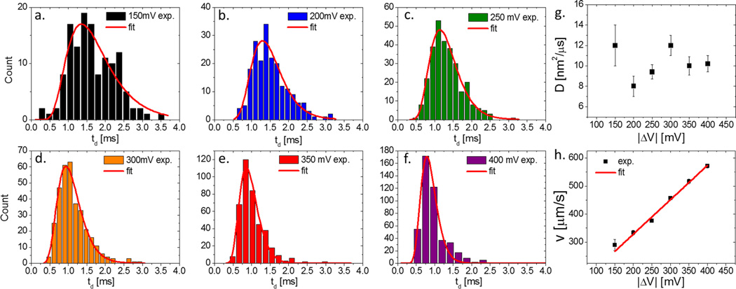
To study the transport properties of nanospheres crossing the nanochannel we performed EONT experiments varying the applied voltage. In Figure 5a–f we show distributions of particle translocation dwell times td determined electrically (see SI for analysis details). Overlaid on the distributions (red curves) are fits to a drift-diffusion model previously used for analyzing DNA and protein transport.17–19 A summary of the obtained values for D and drift velocity v is shown in Figure 5g and h, respectively (scatter plots of the data are shown in the SI). Throughout the voltage range 150–400 mV, we find constant values of D (within error) of 10.0 ± 1.6 nm2/µs, which are only 56% higher than optically extracted mean D values outside the pore and in good agreement with the theoretical value calculated for bulk Brownian diffusion. This agreement is in contrast to our previous findings for protein transport through 5 nm diameter pores, in which D values that are 40 times smaller than bulk were observed.20 Currently, the relation between D in bulk and inside the nanostructure is still under debate. While our data suggests a close similarity in value of D inside and outside the nanostructure, other models that take into account the exact geometry and surface interactions may be necessary for a fully quantitative explanation. In addition, we find that the drift velocity of the nanoparticles increases linearly with voltage, as seen in Figure 5h. From the slope of the fit we obtain the nanoparticle electrophoretic mobility µ, given by µ = v/E, where v is the electrophoretic velocity and E the electric field applied across the nanochannel. Using E = ΔVnano/Leff = 0.71 |ΔV|/Leff (see SI for details), we find µ = 860 ± 50 nm2/ µsV.
Figure 5.
(a–f) Dwell-time distributions of nanospheres’ translocations for different voltages |ΔV| fitted with 1D diffusion-drift model (see SI). (g) Diffusion coefficient D and (h) drift velocity v versus applied voltages |ΔV| calculated from the fits shown in a–f. The red line is the linear fit of the v versus |ΔV| curve.
In conclusion, we have demonstrated here a low-cost, polymer-based device that allows simultaneous determination of a particle’s trajectory before, during, and after voltage-driven transport through a nanochannel. Our EONT method is a simple and powerful tool for studying particle motion in detail and for analyzing more complex samples. By analyzing transport of 40 nm fluorescent particles, we found good agreement between electrically- and optically-determined diffusion coefficients. The possibility of properly functionalizing the surface with probe molecules will further increase the potential of these devices, offering a method for discriminating between interacting and noninteracting nanoparticles, a task which is hard to achieve with simple RPS-based devices or other monomodal measurement systems. Fabrication constraints limit the dimensions of objects measurable with EONT to 20–200 nm. This range includes many objects of biomedical interest (for example, viruses, extracellular vesicles, large macromolecules), and/or nanoparticles and nanopowders that are of great importance in materials science and material safety.
Methods
Device Fabrication
The devices were made entirely of polydimethylsiloxane (PDMS, Sylgard 184, Dow Corning) by replicating the micro and nanofeatures produced on a silicon master, similarly to the approach described in our previous works.14,15 Briefly, conventional photolithography is used to pattern on a Si substrate two pillared U-shaped microchannels whose minimum distance is 100 µm. After conventional lithography, two trapezoidal access areas are created, by means of a focused ion beam (FIB) (CrossBeam by Zeiss), in order to reduce the spacing between the microchannels. Finally, a FIB line scan is performed to pattern a single nanochannel connecting the microchannels. After this direct-write nanopatterning the silicon mold is replicated, by a double replica molding (REM) technique, in a number of polymeric copies each sealed with a glass coverslip; even after bonding the nanochannel is clearly visible (see Figure 1c). An antistiction layer is deposited on the silicon mold in order to promote the detachment of the PDMS negative replica from it. This replica, which reports in negative the features of the silicon master, is treated for 60 s in oxygen plasma (power 30 W), exposed to an antistiction agent, and then replicated with PDMS.
Both negative and positive replicas are made by stacking two PDMS layers with different thickness: the thinner is prepared with a 3:1 prepolymer-curing agent ratio and spin coated on the mold at 1000 rpm for 60 s, while the thicker one is made of PDMS 10:1; both of them are baked in oven at 60 °C for 4 h. Positive replicas are overnight baked at 150 °C, in order to increase the stiffness of the material. After an oxygen plasma treatment (at 30 W for 60 s), the devices are sealed with a thin glass coverslip, to allow the observation of the nanostructures by epifluorescence microscopy. Before sealing, the devices are punched using large needles to allow the insertion of fluid from the back of the device. To apply a bias wire Ag/AgCl electrodes are inserted in two reservoirs filled with an electrolytic solution on the back of the device; see Figure 1a.
Methods
Experimental Setup for EONT Measurements
The scheme of Figure 2a represents the experimental setup that is necessary to simultaneously measure electrical signals and observe fluorescent nanospheres. The device is mounted downward on an inverted epifluorescence microscope (Olympus IX71) provided of a high speed acquisition emCCD camera (Andor iXon 897), a blue laser (Coherent Sapphire, 488 nm, 20 mW) is used to excite the fluorescent nanospheres. Electrodes are connected to an amplifier (Axon Axopatch 200B patch-clamp amplifier) which outputs an analog current signal that is digitized using a National Instruments Data Acquisition (DAQ) system. Electrical and optical signals are synchronized with the camera by means of a TTL signal generated by the DAQ. The traces are then analyzed using a custom MATLAB-based software (see SI).
Fluorescent nanospheres (FluoSpheres 0.040 µm Biotin-Labeled Microspheres F-8766, Invitrogen, Life Technologies) were dispersed in 0.10 M KCl into which 0.1% (v/v) Triton X-100 was added to avoid nanoparticle aggregation. This solution is inserted in one of the two microchannels of the device and during the application of a voltage across the nanochannel nanospheres’ dynamics is observed.
Supplementary Material
Acknowledgments
We acknowledge Andrey Ivankin and Martin Langecker for assistance with data acquisition software, Robert Y. Henley for assistance with signal time-correlation analysis, and Joseph Larkin for carefully reading the manuscript. This work was supported by grants from the National Institutes of Health, R21-HG006873 M.W, and from the Italian Ministry of Education, University and Research, Flagship Project Nanomax and FIRB project Newton RBAP11BYNP_003, U. V.
Footnotes
ASSOCIATED CONTENT
Supporting Information
The authors declare the following competing financial interest(s): Authors E.A., L.R., G.F., P.G., and U.V. declare a financial interest in the company (Nanomed s.r.l.) attempting to commercialize the technology described in this manuscript.
REFERENCES
- 1.Anderson W, Kozak D, Coleman VA, Jämting AK, Trau MJ. Colloid Interface Sci. 2013;405:322–330. doi: 10.1016/j.jcis.2013.02.030. [DOI] [PubMed] [Google Scholar]
- 2.Lane RE, Korbie D, Anderson W, Vaidyanathan R, Trau M. Sci. Rep. 2015;5:7639. doi: 10.1038/srep07639. [DOI] [PMC free article] [PubMed] [Google Scholar]
- 3.Weatherall E, Willmott GR. Analyst. 2015;140:3318–3334. doi: 10.1039/c4an02270j. [DOI] [PubMed] [Google Scholar]
- 4.Dragovic RA, Gardiner C, Brooks AS, Tannetta DS, Ferguson DJP, Hole P, Carr B, Redman CWG, Harris AL, Dobson PJ, Harrison P, Sargent IL. Nanomedicine. 2011;7:780–788. doi: 10.1016/j.nano.2011.04.003. [DOI] [PMC free article] [PubMed] [Google Scholar]
- 5.Yukimoto N, Tsutsui M, He Y, Shintaku H, Tanaka S, Kawano S, Kawai T, Taniguchi M. Sci. Rep. 2013;3:1855. doi: 10.1038/srep01855. [DOI] [PMC free article] [PubMed] [Google Scholar]
- 6.Liu S, Zhao Y, Parks JW, Deamer DW, Hawkins AR, Schmidt H. Nano Lett. 2014;14:4816–4820. doi: 10.1021/nl502400x. [DOI] [PMC free article] [PubMed] [Google Scholar]
- 7.Pagliara S, Schwall C, Keyser UF. Adv. Mater. 2013;25:844–849. doi: 10.1002/adma.201203500. [DOI] [PMC free article] [PubMed] [Google Scholar]
- 8.Pitchford WH, Kim H-J, Ivanov AP, Kim H-M, Yu J-S, Leatherbarrow RJ, Albrecht T, Kim K-B, Edel JB. ACS Nano. 2015;9(2):1740–1748. doi: 10.1021/nn506572r. [DOI] [PubMed] [Google Scholar]
- 9.Soni GV, Singer A, Sun Y, Yu Z, Meller A. Rev. Sci. Instrum. 2010;81:014301. doi: 10.1063/1.3277116. [DOI] [PMC free article] [PubMed] [Google Scholar]
- 10.Ivankin A, Henley RY, Larkin J, Carson S, Toscano ML, Wanunu M. ACS Nano. 2014;8(10):10774–10781. doi: 10.1021/nn504551d. [DOI] [PMC free article] [PubMed] [Google Scholar]
- 11.Anderson BN, Assad ON, Gilboa T, Squires AH, Bar D, Meller A. ACS Nano. 2014;8(11):11836–11845. doi: 10.1021/nn505545h. [DOI] [PMC free article] [PubMed] [Google Scholar]
- 12.Innes LM, Chen C-H, Schiel M, Pevarnik M, Haurais F, Toimil-Molares ME, Vlassiouk I, Theogarajan L, Siwy ZS. Anal. Chem. 2014;86(20):10445–10453. doi: 10.1021/ac502997h. [DOI] [PMC free article] [PubMed] [Google Scholar]
- 13.Pevarnik M, Healy K, Toimil-Molares ME, Morrison A, Létant SE, Siwy ZS. ACS Nano. 2012;6(8):7295–7302. doi: 10.1021/nn302413u. [DOI] [PubMed] [Google Scholar]
- 14.Fanzio P, Manneschi C, Angeli E, Mussi V, Firpo G, Ceseracciu L, Repetto L, Valbusa U. Sci. Rep. 2012;2:791. doi: 10.1038/srep00791. [DOI] [PMC free article] [PubMed] [Google Scholar]
- 15.Manneschi C, Fanzio P, Ala-Nissila T, Angeli E, Repetto L, Firpo G, Valbusa U. Biomicrofluidics. 2014;8(6):064121. doi: 10.1063/1.4904008. [DOI] [PMC free article] [PubMed] [Google Scholar]
- 16.DeBlois RW, Bean CP. Rev. Sci. Instrum. 1970;41:909–916. [Google Scholar]
- 17.Talaga DS, Li JL. J. Am. Chem. Soc. 2009;131:9287–9297. doi: 10.1021/ja901088b. [DOI] [PMC free article] [PubMed] [Google Scholar]; Talaga DS, Li JL. J. Am. Chem. Soc. 2009;131:9287–9297. doi: 10.1021/ja901088b. [DOI] [PMC free article] [PubMed] [Google Scholar]; Talaga DS, Li JJ. J. Am. Chem. Soc. 2013;135:13220. [Google Scholar]
- 18.Li J, Talaga DS. J. Phys.: Condens. Matter. 2010;22:454129. doi: 10.1088/0953-8984/22/45/454129. [DOI] [PMC free article] [PubMed] [Google Scholar]
- 19.Ling DY, Ling XS. J. Phys.: Condens. Matter. 2013;25:375102. doi: 10.1088/0953-8984/25/37/375102. [DOI] [PMC free article] [PubMed] [Google Scholar]
- 20.Larkin J, Henley R, Muthukumar M, Rosenstein J, Wanunu M. Biophys. J. 2014;106:696–704. doi: 10.1016/j.bpj.2013.12.025. [DOI] [PMC free article] [PubMed] [Google Scholar]
Associated Data
This section collects any data citations, data availability statements, or supplementary materials included in this article.


