Abstract
High-resolution, conformable phase masks provide a means to fabricate, in an experimentally simple manner, classes of 3D nanostructures that are technologically important but difficult to generate in other ways. In this approach, light passing through a phase mask that has features of relief comparable in dimension to the wavelength generates a 3D distribution of intensity that exposes a photopolymer film throughout its thickness. Developing this polymer yields a structure in the geometry of the intensity distribution, with feature sizes as small as 50 nm. Rigorous coupled-wave analysis reveals the fundamental aspects of the optics associated with this method; a broad-range 3D nanostructures patterned with it demonstrates its technical capabilities. A nanoporous filter element built inside a microfluidic channel represents one example of the many types of functional devices that can be constructed.
Advances in nanoscience and technology increasingly rely on unconventional techniques for fabricating structures with nanometer dimensions (1–3). Patterning methods that have emerged from the microelectronics industry (photolithography, electron beam lithography, and others) are well suited for patterning 2D structures on ultraflat glass or semiconductor surfaces. Their limited depth of focus, however, makes it challenging to fabricate directly the types of 3D nanostructures that are important for many areas of nanotechnology. New methods based on colloidal sedimentation (4–10), polymer phase separation (11–15), templated growth (16–18), fluidic self-assembly (19, 20), multiple beam interference lithography (21–24), and various approaches based on printing, molding, and writing (1, 3, 25, 26) are all useful for building different classes of 3D nanostructures. Nevertheless, each has limitations in the geometries and sizes of patterns that it can form. Two-photon lithography (27–29) can produce an impressive variety of structures, but its serial operation makes it difficult to pattern large areas or large numbers of structures, although the use of holographic beamsplitters can enable a certain level of parallel operation (30).
Experimental Procedures
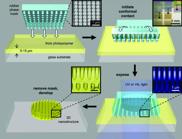
We describe here the optical physics and capabilities of a simple approach that can build a wide variety of complex 3D nanostructures. Fig. 1 shows the procedures. All of the necessary optics are built into a single element: a conformable, elastomeric phase mask with features of relief that have dimensions comparable to the optical wavelength (Fig. 1 Upper Left). Inset shows an angled view scanning electron micrograph (SEM) of the surface of a phase mask. Placing this type of mask against a solid film (5–15 μm thick, formed by spin casting) of a photopolymer (SU-8, Microchem, Newton, MA) leads to intimate physical contact driven by van der Waals forces. This simple procedure aligns the mask to the surface of the photopolymer with atomic scale precision in the z direction (Fig. 1 Upper Right). Complete contact over several square centimeters requires 1 or 2 sec. Passing light through the mask generates a complex 3D distribution of intensity that exposes certain regions of the photopolymer.
Fig. 1.
Schematic illustration of steps for using a high-resolution conformable, elastomeric phase mask to produce 3D nanostructures. Placing such a mask (Upper Left) on the surface of a solid photopolymer film leads to intimate, conformal contact driven by van der Waals forces (Upper Right). (Upper Left Inset) SEM of the surface of a representative mask with relief features in the geometry of a square array of cylindrical posts with a diameter of 375 nm and a height of 420 nm. (Upper Right Inset) Top-view optical micrograph that shows the progression of a “wetting” front that establishes conformal contact between the mask and the underlying photopolymer. Shining light through the mask while it is in contact with the photopolymer film (Lower Right) generates a complex intensity distribution throughout the thickness of the film (Inset), when suitably coherent light is used. Interaction of the light with the polymer results in crosslinking reactions. Washing away the uncrosslinked polymer yields 3D nanostructures whose geometry is defined by the 3D interference pattern formed during exposure (Lower Left). (Lower Left Inset) SEM of a typical structure.
The geometry of this intensity pattern depends on the design (i.e., depth and layout of the relief structures and the index of refraction) of the mask and the wavelength, polarization, and coherence of the exposure light. Relief features with lateral dimensions comparable with the wavelength and with depths sufficient to modulate the phase by a substantial fraction of π can produce submicrometer periodic 3D distributions of intensity with light that has a suitable level of coherence. Inset of Fig. 1 Lower Right shows full vector simulations of this intensity distribution for representative mask geometry with perfectly coherent light. Geometrically collimated light from the spectrally filtered output of a lamp can provide sufficient coherence to form high contrast intensity distributions throughout the thickness (typically, <15 μm) of the photopolymer layers used here. Lasers are, therefore, not required. Furthermore, the van der Waals bond between the mask and the photopolymer prevents any relative motion of these two elements even for long exposure times; external forms of vibration control or isolation are not necessary. As a result, the requirements on the optical setup are minimal. Peeling back the phase mask completes the exposure procedure. Photogenerated acids in the exposed regions of the photopolymer initiate crosslinking reactions at elevated temperatures (75°C for 5–10 min). Washing away the unexposed regions of the polymer with the solvent propylene glycol monomethyl ether acetate (or with a commercial developer obtained from Microchem) and then removing this solvent by drying with supercritical CO2 yields 3D nanostructures that have geometries defined by the intensity pattern (Fig. 1 Lower Left).
Methods
Phase Mask. Photoresist layers patterned on Si wafers by 248-nm projection mode lithography served as “masters” for generating the phase masks. Coating the exposed SiO2 on these wafers by placing them in a perfluorinated trichlorosilane (T2492-KG, United Chemical Technologies, Bristol, PA) vapor in a small vacuum chamber prevented adhesion between the wafers and the silicone elastomers during the casting and curing procedures. A bilayer structure of two types of poly(dimethylsiloxane) (PDMS) was used to replicate the demanding mask geometries, which have relatively tall features but small lateral dimensions. Special care was necessary to form defect-free surface relief structure. The casting began by spin coating a thin film of a high modulus (10 MPa) type of PDMS (VDT-731, HMS-301, Gelest, Morrisville, PA) on the “master” at 1,000 rpm for 40 sec. Allowing the wafer to continue to spin at 500 rpm for 30 min enabled uniform wetting and partial crosslinking of the PDMS. Extremely smooth surfaces can be obtained in this manner. Pouring a prepolymer to another low modulus (2 MPa) form of PDMS (Sylgard 184, Dow-Corning) on top of the first layer generated a 4- to 5-mm-thick soft backing for easy handling of the mask. Fully curing (≈75°C for 1 h) the bilayer PDMS element and peeling it away from the master yielded a conformable phase mask. The layout of the relief features on the mask defines the geometry of features in the photopolymer along the horizontal direction. These relief features can be defined with nanometer precision by using the procedures described above. The distortions in the mask can be held to <4 μm over areas as large as 6 × 6 inches, with optimized designs that use rigid backing layers (31).
Super Critical Drying (SCD). SCD is a well known technique for avoiding the destructive effects of surface tension during drying of fragile structures. It is used extensively in the fabrication of free-standing microelectromechanical structures. We found that this drying procedure improved significantly the quality of the 3D nanostructures generated with the phase masks described above. After exposure, the sample was developed for >30 min in developer (SU-8 developer, Microchem) and transferred to a SCD chamber that held fresh developer. After cooling the chamber to –10°C, liquid CO2 was added on top of the developer. The developer was then purged from the chamber under a continuous supply of liquid CO2. Heating drove the liquid CO2 into its critical point (31.1°C, 7,382 kPa). The drying was completed by removing the CO2 as a gas above the critical point.
Microfluidic Channel. Swelling of the SU-8 by the developer can induce delamination from glass substrate. In addition, the adhesion between the glass substrate and SU-8 layer is not strong enough to withstand the thermal stresses that build up from differences in the coefficients of thermal expansion and the thermal cycling during the SCD step. To avoid these problems, we used a layer of 5-μm-thick film of SU-8 spin-cast and flood-exposed on the glass. This layer effectively improved adhesion of the patterned SU-8 layer to the substrate and prevented delamination during any point in the processing. Before depositing this first uniform layer, we first treated the coverglass (Corning) substrate with O2 reactive-ion etching (RIE) for 5 min [30 mtorr (1 torr = 133 Pa), 100 W, 790 Series, Unaxis, St. Petersburg, FL]. Immediately after RIE, the 5-μm-thick SU-8 film was spin-coated (3,000 rpm, 30 sec) and soft-baked (5 min, 95°C). Afterward, it was flood-exposed (200 mJ/cm2) and hard-baked at 180°C for 5 min. The surface of this film was then exposed to the same RIE step used to prepare the glass. The SU-8 layer for 3D patterning was applied by spin casting on top of this existing SU-8 film. When casting and soft-baking this thick (25 μm) layer, we often observed significant edge bead (i.e., thick regions near the edges of the substrate) that prevented conformal contact of the phase mask with the film. This edge bead was carefully removed with acetone to enable good contact.
Fabricating of the Y-junction microfluidic structure began with exposure through an amplitude mask that had the geometry of the channels. To define the integrated 3D nanoporous filter, we contacted an amplitude mask with a 200-μm-wide slit to the back side of a thin (2 mm) phase mask. Bringing this composite mask against the substrate and exposing again generated a 3D patterned area in a 200-μm-long region in one of the channels.
After developing, the SU-8 structure was treated with plasma cleaner (Harrick Scientific, Ossining, NY) and placed against a flat piece of PDMS that was also treated with the same plasma cleaner. Heating the sample for 10 min at 70°C formed a strong bond between the PDMS and the SU-8. This bonding step completed the fabrication of a sealed microfluidic system that could be loaded and pumped with fluids. The entire structure was optically transparent, allowing for ease of viewing with an optical microscope. We did not observe any degradation in the 3D structure due to filling, pumping, or drying of water-based suspensions.
Optical Modeling. The modeling used rigorous coupled-wave analysis (RCWA) together with the concepts of Abbe theory in image formation (32). In particular, full vector calculations determined the intensities and phases of diffracted beams that appear in the far field after transmission through the mask. Numerically recombining these beams yielded intensity distributions at any position away from the surface of the mask. This approach ignores near-field effects. Separate finite element calculations of the full solutions to Maxwell's equations for 2D masks (i.e., those with lines and spaces) showed however, that although these effects can be important in certain situations, they are negligible of all cases that we considered here.
For the case of modeling of the defect structure and the large period (>1.5 μm) structures, the computational overhead associated with full RCWA was too high for the calculations to be performed on a desktop computer. The modeling in these cases used simple Fraunhofer diffraction theory with extensions of the procedures that we described previously for computing intensity distributions in the near surface region of the mask. For the results of aperiodic structure modeling, the cutoff filter was chosen to correspond to the effective numerical aperture of the confocal microscope. The approximations built into such a computation prevented accurate modeling, but the results captured, in a semiquantitative way, the trends observed experimentally.
Results and Discussion
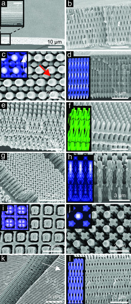
Fig. 2 presents SEM images and modeling results for a broad range of periodic structures that can be fabricated easily and over large areas by using different phase masks and light sources (i.e., visible and UV lasers and mercury lamps). RCWA defines the computed distributions of intensity in each case, as illustrated in the Insets, except for h, i, and j, which were determined by using Fraunhofer analysis to avoid the large computational requirements of RCWA for this case. Qualitatively, the optics of the system can be understood in the following way. Passage of light through a mask that has features of binary relief with lateral dimensions less than or comparable to the wavelength (λ) but larger than ≈λ/4 generates near the surface of the mask (i) deep intensity minima at the recessed regions and step edges and (ii) strong intensity maxima at the raised regions and near these same edges. Both effects arise from the need to maintain continuity in the electric field near abrupt shifts in phase introduced by the mask. The first can be viewed as phase-induced shadowing; the second is a form of focusing from the relief features. This amplitude modulation leads to periodic variations in intensity along z when the light has a sufficient degree of spatial and temporal coherence. An alternative, and consistent, conceptual view is based on the Abbe theory of image formation. It considers the intensity patterns that form when light that appears as diffraction in the far field overlaps and interferes with itself in the region near the mask. In this case, aperture filtering associated with total internal reflection of high-order diffracted light in the mask produces a strong x-, y-, and z-dependent amplitude modulation of the field. Full vector solutions of Maxwell's equations obtained by finite element modeling show that near-field phenomena (as defined by those effects that cannot be predicted by recombination and interference of far-field diffracted light) are insignificant for most of the systems presented here. The distribution of intensity that exists near the surface of the mask recurs periodically along z, consistent with the self-image formation effect (i.e., the Talbot effect). The period associated with this effect depends on the geometry (i.e., the period) of the features of relief on the surface of the mask. For the smallest mask periods, self-image formation can be observed directly in the polymer nanostructures. For exposure light with suitable properties (i.e., coherence, absorption length, and beam size), there is, in principle, no loss of resolution with distance away from the mask, consistent with experimental observations. Applying a step-function cutoff filter to the computed intensity distributions provides a simple way to approximate the crosslinking and developing processes. With such a filter, it is possible to achieve quantitative agreement between the predicted and observed geometries of the polymer nanostructures.
Fig. 2.
SEMs of representative 3D nanostructures. Insets present the corresponding computed optical intensity distributions. In all cases except for one, the conformable phase masks had surface relief in the geometry of a square lattice of isolated raised features with different diameters (d), relief depths (rd), duty cycles (dc), and cross-sectional shapes (i.e., circle, square, etc.). In a–d, d = 375 nm, rd = 420 nm, dc = 35%, and circle (mask 1). In e–f,d = 570 nm, rd = 420 nm, dc = 50%, circle (mask 2). In g–j,d = 1,000 nm, rd = 420 nm, dc = 40%, rounded square (mask 3). In k and l, relief features of lines (300-nm widths) and spaces, rd = 310 nm, dc = 50% (mask 4). The photopolymer layers in all cases had thicknesses of ≈10 μm. The tripled output (355 nm) of a Nd:YAG laser provided light for the exposures in all cases except for d (365-nm light from the filtered output of a mercury lamp) and f (514-nm light from an Ar-ion laser). (a) 3D nanostructure patterned with mask 1 over a large area, limited only by the size of the mask. (Scale bar of Inset, 3 μm.) (b) (110) cross-sectional view of the structure in a. (c) Top view of the same structure (red arrow points to an ≈100-nm structure in width). Inset shows modeling (arrow indicates the direction of polarization of the exposure light). (d) (100) cross-sectional view of a 3D nanostructure formed with mask 1 and the filtered output of the 365-nm emission line from a conventional mercury lamp. The modeling (Inset), which assumes perfect coherence, accounts accurately for the shape of this structure. (e) Structure generated with mask 2 and 355-nm light. (f) Structure generated from mask 2 with 514-nm laser light. The top layer of this structure, which is shown in the modeling, peeled off because of its thin connecting features to the underlying structure. (g) Structure generated with mask 3. (h) Close-up view of tilted (100) facet of this structure. The modeling in the inset corresponds to a cross-section cut through the middle of the pillars. (i) Magnified view of top surface of this structure; Inset shows modeling results. (j) Bottom surface, with Inset modeling. (k) Stack of sealed nanochannels made by using mask 4. The polarization direction is parallel to line (arrow). (l) Magnified cross-sectional view, with Inset modeling.
As shown in Fig. 2, patterns that range from interdigitated cylindrical structures, to arrays of complex structured hollow posts, to stacks of sealed nanochannels can be produced and modeled accurately. We did not observe, as expected based on the Talbot effect, any loss of resolution through the thickness of the resist. The upper limit in the thickness of the structures is defined mainly by the properties of the photopolymer (physical strength, optical absorption, swelling, etc.) and not by the optics. We have patterned layers as thick as 30 μm. The smallest features have dimensions of ≈100 nm (i.e., post diameters and line widths; see red arrow in Fig. 2) and, in some cases, 50 nm. The wavelength of the exposure light in the photopolymer (and to some extent the processing conditions) determines the highest spatial frequencies. For a given mask, films exposed with green (514 nm from an argon ion laser) light (Fig. 2f) yield patterns with less fine structure than those exposed with UV light (Fig. 2e). Patterns generated with UV laser light [355-nm tripled output from a neodymium doped yttrium aluminum garnet (Nd:YAG) laser] differ from those generated with the geometrically collimated (by passage through a black tube with a diameter of 3 mm and a length of 17 cm) and spectrally filtered (2-nm bandwidth centered at 365 nm; ASC i-line filter, Omega Optical, Brattleboro, VT) output of a conventional mercury lamp (Mercury Lamp 87230, Oriel, Stamford, CT) in subtle ways that can be fully accounted for by the difference in wavelength. Effects of partial coherence (the temporal coherence length is ≈20 μm for this case) of the filtered light from the lamp are negligible in all cases that we examined.
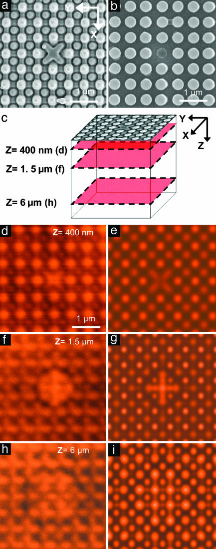
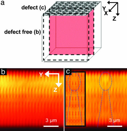
The soft lithographic casting and curing procedures that form the conformable phase masks provide considerable flexibility in the design of these elements. In addition to the periodic masks used for the structures shown in Fig. 2, aperiodic systems are also possible. Figs. 3 and 4 present, as an example, results from a mask that includes a “defect” structure (i.e., a missing post) in a square lattice of cylindrical posts. A series of images collected with a confocal microscope reveals the full 3D shape of this polymer nanostructure. Good agreement is observed with simple modeling that uses Fraunhofer diffraction theory. This level of understanding of the optics suggests a path toward the design of specialized masks for generating intensity distributions that approximate certain desired geometries.
Fig. 3.
SEM, schematic, confocal micrographs (Leica SP2), and optical modeling illustrating the geometry of an aperiodic structure made with a specially designed conformable phase mask. (a) SEM image of the surface of a 3D nanostructure formed by using mask 1 with an isolated missing post. (b) Topview SEM image of this mask. (c) 3D perspective view of x–y cross-sectional plane. (d–i) Confocal image of x–y plane and modeling at z depths of 400 nm (d and e), 1.5 μm(f and g), and 6 μm(h and i).
Fig. 4.
Schematic, confocal micrographs, and optical modeling of aperiodic structure in x–z plane. (a) Three-dimensional perspective view of x–z cross-sectional plane. (b) Confocal micrograph of the x–z plane of the structure imaged at a position y that is far from the missing post (i.e., defect structure). (c) Similar image collected at the location of the defect. Inset shows modeling results. The dotted line highlights certain features.
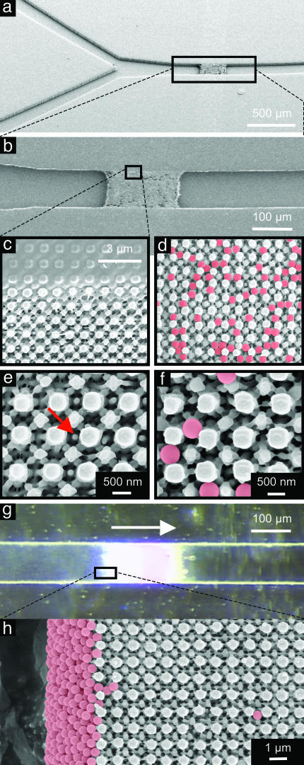
The practical utility of such 3D nanostructures depends critically on their mechanical robustness and the ability to integrate them with microsystems and larger-scale components to produce functional devices. To illustrate these features, we built a 3D nanostructured filter element integrated into a microfluidic system for separating submicrometer particles from fluid flows. Fig. 5 illustrates the structure. Even the smallest parts of these structures are mechanically robust to wetting and dewetting of aqueous solutions and to pressure-driven flow. Flowing a suspension of polystyrene beads (500-nm diameter) through this filter allows the fluid, but not the beads, to pass through the nanopores. The SEM images shown in Fig. 5 d, f, and h show blockage of the beads. The optical image in Fig. 5g shows cloudy fluid with suspended beads to the left of the filter and clear fluid without beads on the right.
Fig. 5.
SEMs and optical micrographs of a 3D nanostructure built into the channel of a microfluidic system. The mask consists of a square array of relief features with diameters of 740 nm (rounded square), a relief depth of 420 nm, and a duty cycle of 43%. (a)A45° tilted view of Y-junction channel (channel width of 100 μm). (b) Magnified SEM view of 3D structure integrated into a fluidic channel. (c) Magnified view of the region near the edge of the channel. (d) Five-hundred-nanometer particles (F8812, FluoSpheres, Molecular Probes) filtered through a 3D structure. The beads are colorized for ease of viewing. (e) Magnified view of top surface structure. The red arrow indicates an ≈100-nm nanostructure. (f) Magnified view of d. (g) Flowing an aqueous suspension of 0.02% beads into the channel at the rate of 3 μl/min (arrow indicates flow direction) results in a filtering of the beads. (They remain on the left side of the filter.) (h) Filtered beads at the side wall because of the flow direction.
The simplicity of the optics afforded by the conformable phase masks and the wide range of periodic and aperiodic structures that can be produced are two attractive characteristics of this approach to 3D nanopatterning. It is these two features that distinguish this technique from its most similar alternative: multiple-beam interference lithography. The application of this method to other photosensitive materials and the use of the 3D structures as sacrificial templates (5, 7, 17) both provide means to pattern various material types. Incorporating amplitude modulating elements (e.g., thin metal films) onto the surface of the phase masks and exploiting reflecting substrates will add considerable additional patterning flexibility. The results here show, using phase-only masks with a range of geometries, some of the types of 3D structures that are possible. We did not attempt to illustrate the more difficult, and potentially more useful, capability of using specially designed phase masks to achieve distributions of intensity for desired 3D structures. This inverse problem is a difficult one without a general solution, because arbitrary 3D structures cannot be encoded into an inherently 2D distribution of phase levels on a mask. Defining the range of structures that will be possible by using phase or phase and amplitude masks, and developing algorithms to define best-fit masks for user-specified 3D structures, is the subject of current work.
A nanoporous filter element built inside a microfluidic channel represents one example of many potential application areas in fluidic systems (i.e., chromatographic separators, mixers, etc.) (33, 34); other areas include photonics (30, 35), sensors (36), catalyst supports (6), and information storage (27). We believe that this general approach will complement or replace existing 3D nanopatterning techniques for building many structures for research and development in nanotechnology, including unusual subwavelength optical filters and ultrathin holographic correlators; high surface-area elements for sensors, catalyst supports, and drug delivery; nanostructured surfaces to control wetting phenomena; and many others.
Acknowledgments
This article is based on work supported by the U.S. Department of Energy, Division of Materials, through the Frederick Seitz Materials Research Laboratory and the Center for Microanalysis of Materials at the University of Illinois at Urbana–Champaign.
This paper was submitted directly (Track II) to the PNAS office.
Abbreviations: PDMS, poly(dimethylsiloxane); SEM, scanning electron micrograph.
References
- 1.Xia, Y., Rogers, J. A., Paul, K. E. & Whitesides, G. M. (1999) Chem. Rev. 99, 1823–1848. [DOI] [PubMed] [Google Scholar]
- 2.Michel, B., Bernard, A., Bietsch, A., Delamarche, E., Geissler, M., Juncker, D., Kind, H., Renault, J. P., Rothuizen, H., Schmid, H., et al. (2001) IBM J. Res. Dev. 45, 697–719. [Google Scholar]
- 3.Mirkin, C. A. & Rogers, J. A. (2001) MRS Bull. 26, 506–509. [Google Scholar]
- 4.Velev, O. D., Jede, T. A., Lobo, R. F. & Lenhoff, A. M. (1997) Nature 389, 447–448. [Google Scholar]
- 5.Park, S. H. & Xia, Y. (1998) Chem. Mater. 10, 1745–1747. [Google Scholar]
- 6.Holland, B. T., Blanford, C. & Stein, A. (1998) Science 281, 538–540. [DOI] [PubMed] [Google Scholar]
- 7.Jiang, P., Cizeron, J., Bertone, J. F. & Colvin, V. L. (1999) J. Am. Chem. Soc. 121, 7957–7958. [Google Scholar]
- 8.Vlasov, Y. A., Bo, X. Z., Sturm, J. C. & Norris, D. J. (2001) Nature 414, 289–293. [DOI] [PubMed] [Google Scholar]
- 9.Dinsmore, A. D., Hsu, M. F., Nikolaides, M. G., Marquez, M., Bausch, A. R. & Weitz, D. A. (2002) Science 298, 1006–1009. [DOI] [PubMed] [Google Scholar]
- 10.Murray, C. (1998) MRS Bull. 23, 33–38. [Google Scholar]
- 11.Bates, F. S. (1991) Science 251, 898–905. [DOI] [PubMed] [Google Scholar]
- 12.Park, M., Harrison, C., Chaikin, P. M., Register, R. A. & Adamson, D. H. (1997) Science 276, 1401–1404. [Google Scholar]
- 13.Boltau, M., Walheim, S., Mlynek, J., Krausch, G. & Steiner, U. (1998) Nature 391, 877–879. [Google Scholar]
- 14.Kim, S. O., Solak, H. H., Stoykovich, M. P., Ferrier, N. J., de Pablo, J. J. & Nealey, P. F. (2003) Nature 424, 411–414. [DOI] [PubMed] [Google Scholar]
- 15.Fink, Y., Urbas, A. M., Bawendi, M. G., Joannopoulos, J. D. & Thomas, E. L. (1999) J. Lightwave Technol. 17, 1963–1969. [Google Scholar]
- 16.Furneaux, R. C., Rigby, W. R. & Davidson, A. P. (1989) Nature 337, 147–149. [Google Scholar]
- 17.Martin, C. R. (1995) Acc. Chem. Res. 28, 61–68. [Google Scholar]
- 18.Trau, M., Yao, N., Kim, E., Xia, Y., Whitesides, G. M. & Aksay, I. A. (1997) Nature 390, 674–676. [Google Scholar]
- 19.Jacobs, H. O., Tao, A. R., Schwartz, A., Gracias, D. H. & Whitesides, G. M. (2002) Science 296, 323–325. [DOI] [PubMed] [Google Scholar]
- 20.Yeh, H. J. J. & Smith, J. S. (1994) IEEE Photon. Technol. Lett. 6, 706–708. [Google Scholar]
- 21.Campbell, M., Sharp, D. N., Harrison, M. T., Denning, R. G. & Turberfield, A. J. (2000) Nature 404, 53–56. [DOI] [PubMed] [Google Scholar]
- 22.Yang, S., Megens, M., Aizenberg, J., Wiltzius, P., Chaikin, P. M. & Russel, W. B. (2002) Chem. Mater. 14, 2831–2833. [Google Scholar]
- 23.Divliansky, I., Mayer, T. S., Holliday, K. S. & Crespi, V. H. (2003) Appl. Phys. Lett. 82, 1667–1669. [Google Scholar]
- 24.Ullal, C. K., Maldovan, M., Thomas, E. L., Chen, G., Han, Y.-J. & Yang, S. (2004) Appl. Phys. Lett. 84, 5434–5436. [Google Scholar]
- 25.Quake, S. R. & Scherer, A. (2000) Science 290, 1536–1540. [DOI] [PubMed] [Google Scholar]
- 26.Smay, J. E., Cesarano, J., III, & Lewis, J. A. (2002) Langmuir 18, 5429–5437. [Google Scholar]
- 27.Cumpston, B. H., Ananthavel, S. P., Barlow, S., Dyer, D. L., Ehrlich, J. E., Erskine, L. L., Heikal, A. A., Kuebler, S. M., Lee, I. Y. S., McCord-Maughon, D., et al. (1999) Nature 398, 51–54. [Google Scholar]
- 28.Kawata, S., Sun, H.-B., Tanaka, T. & Takada, K. (2001) Nature 412, 697–698. [DOI] [PubMed] [Google Scholar]
- 29.Galajda, P. & Ormos, P. (2001) Appl. Phys. Lett. 78, 249–251. [Google Scholar]
- 30.Grier, D. G. (2003) Nature 424, 810–816. [DOI] [PubMed] [Google Scholar]
- 31.Menard, E., Bilhaut, L., Zaumseil, J. & Rogers, J. A. (2004) Langmuir 20, 6871–6878. [DOI] [PubMed] [Google Scholar]
- 32.Klein, M. V. (1970) Optics (Wiley, New York).
- 33.Xie, S., Allington, R. W., Frechet, J. M. J. & Svec, F. (2002) Adv. Biochem. Eng./Biotechnol. 76, 87–125. [DOI] [PubMed] [Google Scholar]
- 34.Kenis, P. J. A., Ismagilov, R. F. & Whitesides, G. M. (1999) Science 285, 83–85. [DOI] [PubMed] [Google Scholar]
- 35.Christodoulides, D. N., Lederer, F. & Silberberg, Y. (2003) Nature 424, 817–823. [DOI] [PubMed] [Google Scholar]
- 36.Holtz, J. H. & Asher, S. A. (1997) Nature 389, 829–832. [DOI] [PubMed] [Google Scholar]


