Abstract
In this work, we report on a simple non-injection synthesis routine for the preparation of well-dispersed monocrystalline Cu2ZnSnS4 (CZTS) nanoparticles (NPs). The nanocrystal morphology was investigated by scanning and transmission electron microscopy, and its phase composition was studied by X-ray diffraction and Raman analyses. Cu2ZnSnS4 nanoparticles prepared using ethanolamine and diethanolamine as chemical stabilizers showed a high purity and a suitable size for polymer solar cell applications. The fabricated CZTS NPs are shown to be easily dispersed in a polymer/fullerene aromatic solution as well as the hybrid photovoltaic active layer. Thanks to the increment in the light absorption and electrical conductivity of the active layer, solar cells with a small amount of CZTS nanoparticles resulted in a clear enhancement of the photovoltaic performance. The short-circuit current density is increased from 9.90 up to 10.67 mA/cm2, corresponding to an improvement in the power conversion efficiency (PCE) from 3.30 to 3.65%.
Keywords: Nanocrystalline material, Cu2ZnSnS4, Solvothermal method, Photoelectrochemical property
Background
Bulk heterojunction (BHJ) polymer solar cells (PSCs) have gained interest due to their light weight, flexibility, and low-cost fabrication by using solution-processing methods [1–3]. Recently, PSCs with a high power conversion efficiency (PCE) of ~10% have been fabricated in laboratories by many groups by employing new organic photovoltaic materials including conducting polymers [4, 5] and non-fullerene (NF) acceptors [6]. Nerveless, the large-scale fabrication of commercially viable PSCs is still unsatisfactory [7, 8]. Large-scale preparation methods such as conventional doctor-blading, brush-painting, spray-coating, screen, and ink-jet printing cannot provide as efficient PSCs as laboratory-derived spin-coated photovoltaic devices. This is mainly due to the fact that these methods mentioned above are deficient for the deposition of thin organic films (100–300 nm) with the desired morphology. Typically, in a BHJ solar cell, the active layer is composed of a conjugated polymer electron donor and an organic electron acceptor compound sandwiched by interfacial layers and patterned electrodes. The active material and the interfacial contact are crucial aspects determining the photovoltaic device performance. Compared to inorganic photovoltaic materials, conducting polymers usually display sensibly lower carrier mobility. The active layer should thus be designed to be very thin in order to separate positive and negative charge carriers and collect them efficiently at the respective metal electrodes [9].
It is well-known that the charge photogeneration in PSCs can be divided into four steps: light absorption (A), exciton diffusion (ED), charge separation (CS), and charge collection (CC). The photon conversion efficiency of a PSC (η) can be thus described as the product of all processes efficiencies: η(PCE) = η A × η ED × η CS × η CC[10]. The decrease of active layer thickness enhances η CC while it lowers η A in the visible light. This is the typical reason why PSCs usually have a lower current density (J SC) compared to inorganic solar cells. To overcome this limitation, nanostructures or nanomaterials have been employed for increasing the PCE in donor/acceptor material systems. One of the most effective ways which was reported to improve the J SC in a thin polymer active layer is by increasing the contact interface between the active layer and the buffer layer by using ZnO-based nano-ridges or nano-flakes [11, 12]. However, Liang et al. suggested that voids can occur at the interface when ZnO has a rough surface, resulting in an increased series resistance (R S) and deceased shunt resistance (R SH) [13]. Inorganic nanocrystals (NCs) are appealing candidates for increasing both the absorption rate and the electrical conductivity of an active layer. Luszczynska et al. [14] have obtained an improvement of the maximum external quantum efficiency from 48 to 70% for a P3HT/PC61BM bulk heterojunction by adding Cu–In–Se NCs into the P3HT:PCBM blend. Their following work showed an improved photovoltaic performance for P3HT:PCBM solar cells by adding CuInS2 NCs [15]. Although the PCE was limited, the addition of metal sulfide NPs into the polymer resulted in an encouraging enhancement of the light-harvesting ability and J SC (from 3.47 to 6.34 mA/cm2). Luan et al. [16] also have improved the PCE of P3HT:PCBM solar cells from 2.8 to 3.0% with adding a mount FeS2. The deficiency was the Low FF of the PSCs which was possibly influenced by the rough surface and poor disperse of the NPS. By optimizing the active layer morphology, there is still room for improving the PSC performance and in particular for the fill factor.
In this study, we demonstrate that the photovoltaic properties of a PSC can be improved by adding solvothermally synthesized monocrystalline Cu2ZnSnS4 (CZTS) NPs into the P3HT:PCBM active layer. The peculiarity of this study is that we have employed an advanced N2 protected ultrasonic spray system for improving the deposition of the hybrid organic–inorganic active layer. Firstly, we will introduce our simple and low-toxicity solvothermal method for the synthesis of single-phase monocrystalline CZTS NPs. These NPs can be well-dispersed in aromatic precursor solutions. The successful preparation of high-quality CZTS NPs results to rely mostly in choosing the appropriate chemical stabilizer and preparing the precursor solution in the right order. Thanks to the increase in the light absorption efficiency and to the higher electron mobility (~5 cm2 V−1 s−1) [17, 18], the PSC with CZTS NPs exhibited a considerable increase in the J SC and the external quantum efficiency (EQE).
Methods
Preparation of CZTS NPs
A mixed solvent containing 40 mL ethanol, 1.5 mL diethanolamine, and 1 mL acetate was firstly prepared. Then, 0.5 mmol CuCl2·2H2O, 0.25 mmol Zn(CH3COO)2·2H2O, 0.25 mmol SnCl2·2H2O, and 1 mmol thiourea were added to the solvent under magnetic stirring. The mixture turned into a bright blue solution after the addition of 1.5 mL ethanolamine. Then, the mixture was diluted by 120 mL ethanol and transferred into 50 mL para poly phenol (PPL) lined stainless steel autoclaves with a capacity of 32 mL (80% capacity). The autoclaves were heated at 240 °C for 24 h and then naturally cooled down to room temperature. The final product was centrifuged at 13,000 rpm for 30 min and washed with ethanol repeatedly for at least three times, followed by a drying at room temperature in a vacuum oven. In order to highlight the role of the chemical stabilizer on the phase composition and morphology, three chemical stabilizers (ethanolamine, oleylamine, and diethanolamine) with specific ratios were investigated.
Fabrication and Testing of Photovoltaic Devices
Glass/indium tin oxide (ITO) substrates were cleaned stepwise in an ultrasonic bath containing a detergent, acetone, deionized water, and ethanol (each step for 10 min) and then dried with nitrogen. The preparation steps of CZTS/polymer solar cells are shown in Fig. 1c. A 50-nm ZnO layer was grown on the ITO by using the previously reported ultrasonic spray pyrolysis method at 200 °C [19, 20]. Consecutively, the precursor solution was deposited by spray coating to form a ~350-nm-thick absorber layer by using an ultrasonic spray system (nozzle: Siansonic Z95S). The active polymer solution was prepared by dissolving 5 mg P3HT (Rieke Metals) and 5 mg PCBM (Nano-C) in 1 mL o-dichlorobenzene (ODCB). Subsequently, different concentrations of CZTS NPs were added to the solution. Before the active layer deposition, hybrid solutions were sonicated for at least 30 min. A MoOx film (8 nm) and an Ag film (150 nm) were then successively thermally evaporated onto the hybrid blend at a pressure below 10−4 Pa. Four samples were prepared in a process, each sample having five cells with an active area of 0.06 cm2
Fig. 1.
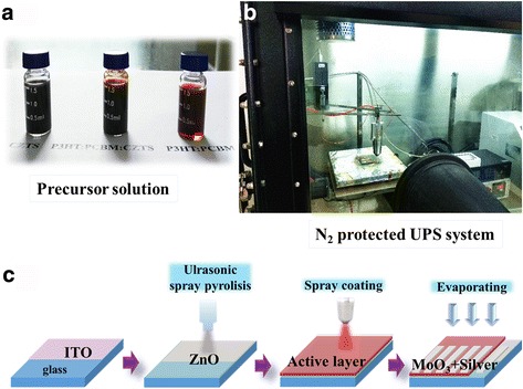
a CZTS NCs and P3HT:PCBM dispersed in o-DCB solution. b Glove-box protected ultrasonic spray system. c Fabrication process of photovoltaic devices
Characterization of CZTS Nanocrystals and Layers
The composition and crystal structure were characterized by X-ray diffraction (XRD, Bruker D8) in a conventional mode. The nanoscale information of CZTS NPs and blend absorbers were characterized by scanning electron microscopy (SEM, Zeiss Merlin) and high-resolution transmission electron microscopy with selected-area electron diffraction (SRED) (HRTEM; Zeiss Libra200). The NC composition was characterized by Raman spectroscopy (LabRam HR800 UV, Horiba Jobin-Yvon) with an excitation wavelength of 514 nm. Optical transmittance spectra in the 340–720 nm wavelength range were carried out on blend films by using a UV-Vis-IR spectrophotometer (Agilent Cary 5000). The film thickness was measured by a stylus profilometer (Alpha-Step D-100). Current density–voltage (J–V) characteristics of photovoltaic devices were recorded with a Keithley 2400 under a xenon lamp (7IS0503A, Beijing SOFN) with an illumination power of 100 mW/cm2. The external quantum efficiency (EQE) was measured using an integrated system (7-SCSpecIII, Beijing SOFN) and a lock-in amplifier with a current preamplifier under short-circuit conditions.
Results and Discussion
Crystal Structure and Composition of NPs Using Different Chemical Stabilizers
For the conventional solvothermal method, the difficulty is to obtain single-phase monocrystalline NPs from a solution including Cu+, Zn2+, and Sn4+ cations. One function of the chemical stabilizer is to promote the cation dissolution in alcohols. An even more important role is to modulate the cation crystallization temperature. As we see in the SEM image Fig. 2a, by using the precursor with 3 mL pure ethanolamine chemical stabilizer, a multiphase final product showing different grain shapes was obtained. When the chemical stabilizer was replaced by 1.5 mL ethanolamine + 1.5 mL oleylamine, or 1.5 mL ethanolamine + 1.5 mL diethanolamine, final products with different grain sizes were obtained. Remarkably, when using a mixture of ethanolamine and diethanolamine, NPs displayed a consistent shape and a suitable size for being dispersed in the active photovoltaic layer. With other stabilizers, the NP size was even larger than the target thickness of the active layer.
Fig. 2.
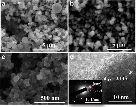
SEM image of as-synthesized nanoparticles using different chemical stabilizers: a 3 mL ethanolamine, b 1.5 mL ethanolamine + 1.5 mL oleylamine, c 1.5 mL ethanolamine + 1.5 mL diethanolamine, and d HRTEM image with SRED of the sample in c
XRD patterns are shown in Fig 3a. Main diffraction peaks ascribed to the (112), (220), and (312) planes of CZTS are easily identified all the three patterns. Since lattice parameters of CZTS are close to those in CuSnS3 (CTS) and ZnS, it is difficult to distinguish among these compounds by looking at diffraction peaks. However, several CTS- and ZnS-related diffraction peaks can be obviously identified in the nanopowder synthesized by using ethanolamine or the ethanolamine and oleylamine mixture as a chemical stabilizer. Raman analysis provides for a more univocal composition assignment as shown in Fig. 3b. Two CZTS Raman peaks at 332 and 285 cm−1 are detected, in good agreement with previously reported results [21], confirming that each of the three powder samples is mainly composed of CZTS. It is worth noting that, in agreement with XRD results, CTS and ZnS Raman modes, respectively, at 361 cm−1 and 653 cm−1, were simultaneously found only in samples synthesized using ethanolamine or the ethanolamine/oleylamine mixture as a chemical stabilizer.
Fig. 3.
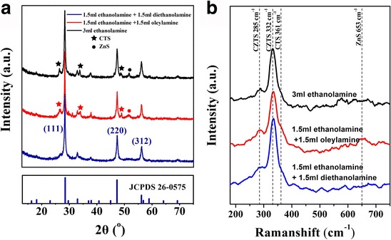
XRD patterns (a) and Raman spectra (b) of as-synthesized NPs using different chemical stabilizers
According to our experience, single-phase and well-dispersed CZTS NPs can be achieved using the binary chemical stabilizer system composed of ethanolamine and diethanolamine with a 1:1 volume ratio. As shown in Fig 3b, when the 1.5 mL ethanolamine and 1.5 mL diethanolamine chemical stabilizer was used, no other characteristic peaks from impurities were observed in the Raman spectrum. In Fig. 2a, the SEM image shows a consistent NP shape with an average grain size of about 50 nm. Figure 2d shows the HRTEM image and SRED pattern of CZTS NPs. The HRTEM image shows that NPs have clear lattice fringes with an interplanar spacing of 3.14 Å; this was ascribed to the (112) plane and well agrees with the XRD peak at 28.6o (Fig. 2a), demonstrating the crystalline nature of CZTS NCs. SRED pattern is composed by periodically arranged diffraction spots consistent with the CZTS lattice, indicating the CZTS domains are monocrystalline. In addition, the composition and the average grain size are appropriate for the absorber layer fabrication. As-synthesized CZTS NPs were dispersed in P3HT:PCBM solution following the scheme in Fig. 1a. In the deposition process, an ultrasonic spray system was employed to provide for a higher curing rate for the hybrid solute at a very low N2 flow rate. Accordingly, polymer-wrapped particles do not diffuse during solvent evaporation. If a spin-coating method was used, NPs would tend to move to the wafer edge under the centrifugal force, resulting in an inhomogeneous final NP dispersion and surface morphology. As shown in Fig. 4b, the ultrasonic spray deposition resulted in well-dispersed CZTS NPs into the active blend layer. The cross-sectional SEM of the active layer shows a homogeneous NP dispersion and a uniform thickness. This resulted in devices which were not susceptible to short circuits and with a good yield of more than 95% (for CZTS ≤2 mg/mL).
Fig. 4.
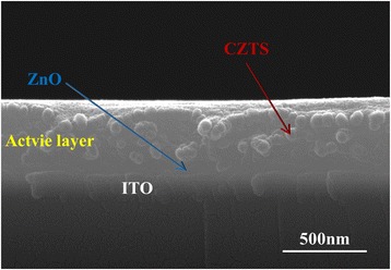
Cross-sectional SEM image of P3HT:PCBM:CZTS hybrid blend film deposited by ultrasonic spray
Photovoltaic Performances
Typical J–V characteristics of photovoltaic devices assembled with different monocrystalline CZTS NP concentrations under illumination are shown in Fig. 5. Device performances are summarized in Table 1. The standard device, without NPs, shows an open-circuit voltage (V OC) of 0.61 V, a short-circuit current density (J SC) of 9.90 mA/cm2, a fill factor (FF) of 54.61%, and a PCE of 3.30%. The J SC was obviously improved even with the addition of a small amount CZTS NPs. For a CZTS NP concentration of 1.0 mg/mL, the J SC reached a maximum value of 10.67 mA/cm2. The optimum device performance was obtained for a CZTS NP concentration between 0.5 and 1.0 mg/mL, with a best PCE of 3.65%, corresponding to a 10.6% enhancement with respect to the standard device. Interestingly, for a higher CZTS NP concentration of 1.5 mg/mL, the device performance showed a degradation of the PCE and a lower FF and shunt resistance (R SH). For a higher CZTS NP concentration of 2 mg/mL, the PCE was further reduced to 2.75% with a FF of 48.51%.
Fig. 5.
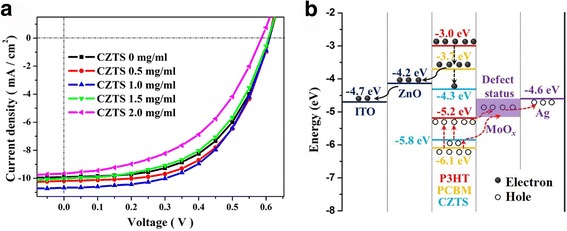
J–V characteristics under illumination (a) and energy levels of the P3HT:PCBM:CZTS hybrid solar cells (b)
Table 1.
Solar cell parameters obtained with different CZTS NP concentrations
| CZTS (mg/mL) | V OC (V) | J SC (mA/cm2) | FF (%) | PCE (%) | R S (Ω cm2) | R SH (Ω cm2) |
|---|---|---|---|---|---|---|
| 0 | 0.61 | 9.90 | 54.61 | 3.30 | 13 | 1565 |
| 0.5 | 0.61 | 10.38 | 56.71 | 3.58 | 11 | 1527 |
| 1.0 | 0.61 | 10.67 | 55.09 | 3.65 | 13 | 1473 |
| 1.5 | 0.61 | 10.21 | 52.86 | 3.27 | 14 | 789 |
| 2.0 | 0.59 | 9.67 | 48.51 | 2.75 | 17 | 629 |
In order to investigate the photovoltaic performance enhancement mechanism, the PSC energy level alignment has been drawn (Fig. 5b). Under light irradiation, both the active polymer and CZTS NPs do absorb photons and generate excitons [18]. Excitons are split into electrons and holes in the P3HT-PCBM and CZTS-PCBM heterojunction interface. Then, electrons are transferred to the PCBM lowest unoccupied molecular orbital (LUMO) level and holes to the P3HT highest unoccupied molecular orbital (HOMO) level of the CZTS. Thanks to the convenient energy level and the high carrier mobility, holes in CZTS can be easily and quickly transported to the MoOx and be collected at the Ag electrode. However, the LOMO level of CZTS (−4.3 eV) is lower than that of ZnO (−4.2 eV), meaning that electrons in the CZTS are blocked from transporting the cathode, resulting in the accumulation of electron in the active layer [16, 22]. When a small amount of CZTS (~1 mg/mL) is added to the active layer, the advantage of carrier’s generation was greater than its deficiency in carrier transmission. Therefore, the device acquired a subsequent higher J SC and quantum efficiency. On the other hand, when the active layer had more CZTS NPs (i.e., 2 mg/mL), the electron transport deficiency effect could not be any more ignored. Carrier recombination rate reaches to an unfavorable level; thus, the device PCE declined gradually with the obviously drop of R SH.
To study the light-harvesting performance, the light absorption and the EQE were simultaneously tested. According to the EQE spectrum shown in Fig. 6a, devices with 0.5 to 1.0 mg/mL CZTS NPs result in a clear improvement in the EQE. The EQE increment is thought to rely mostly on the higher light absorbance. As shown in Fig. 6b, the blend film UV-Vis-IR absorbance shows a gradual increment with the CZTS NP content. The EQE increment was observed at almost all the entire tested wavelength range; this is ascribed to the higher light absorption in the broad (400–1000 nm) spectral range [21, 23], indicating CZTS NPs modify the light-harvesting capability of the P3HT:PCBM layer.
Fig. 6.
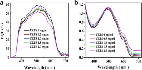
a EQE of solar cells and b UV-Vis-IR absorption spectrum of blend films containing different concentrations of CZTS NPs
It is well-known that the interface between active layer and metal electrode is crucial to the carrier’s collection [24]. AFM was used to observe how the morphology of blend active layer is affected by CZTS NP concentration. AFM images allow displaying the 3D topography and extracting the surface roughness (Fig. 7). The root mean square (RMS) roughness value is 1.05 nm in the bare P3HT:PCBM film, and it increases with the CZTS NP concentration when this is varied from 0.5 to 2.0 mg/mL. However, the RMS value increase is weak, as the roughest surface was only 1.56 nm, which is much lower what previously reported for P3HT:PCBM:FeS2 films [16]. When the NP concentration is 1.5 and 2.0 mg/mL, some aggregated particle ridges appear at the surface of the active layer. Although a low increase in the surface roughness can be beneficial to the light absorption [25, 26], due to the presence surface defects acting as recombination sites for the photo-generated charge, charges tend to be captured by these aggregated particle ridges rather than be transported to the metal electrode [27], resulting to a lower R SH and a lower FF in the solar cell. We think that this is an additional cause leading to the degradation of devices with a large CZTS NP concentration.
Fig. 7.
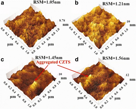
AFM image of blend films with different CZTS NP concentrations. a 0 mg/mL. b 0.5 mg/mL. c 1.5 mg/mL. d 2.0 mg/mL
Conclusions
High-quality and well-dispersed CZTS nanoparticles have been successfully prepared by a solvothermal method using an appropriate chemical stabilizer containing ethanolamine and diethanolamine with the volume ratio of 1:1. As-synthesized CZTS NPs resulted to be well-dispersed in a hybrid polymer/fullerene aromatic solution as well as in spray-deposited hybrid active layers. By adding a small amount of CZTS to photovoltaic active layers, the hybrid device resulted in an enhanced light-harvesting ability and a 10.6% enhancement of the PCE with respect to the reference device without CZTS NCs. This approach has the advantage of being environmental friendly, cost-effective, and compatible with large-scale production.
Acknowledgements
The authors thank Dr. Xian (Siansonic Technology Co.) for the spray technical support and Co-Innovation Center for Micro/Nano Optoelectronic Materials and Devices for the financial support.
Funding
This work was supported by the National Natural Science Foundation of China (Grant No. 61505018), Technology Project from Chongqing Education Committee (Grant No. KJ1401113), and Chongqing University of Arts and Science (Grant No. R2012CJ18).
Authors’ Contributions
CJ designed and conducted the experiments and analyses and drafted the manuscript. ZD and BC prepared the CZTS NPs and performed the characterization of CZTS nanocrystals. RJ fabricated the photovoltaic devices and performed the photoelectrochemical measurement. YX and HR provided the technical support and conceptual advice. JZ and LL modified the manuscript and supervised all the projects. All authors read and approved the final manuscript.
Competing Interests
The authors declare that they have no competing interests.
Declarations
This study has nothing to do with human participants or health-related outcomes.
Abbreviations
- AFM
Atomic force microscope
- BHJ
Bulk heterojunction
- CTS
CuSnS3
- CZTS
Cu2ZnSnS4
- EQE
External quantum efficiency
- HOMO
Highest unoccupied molecular orbital
- HRTEM
High-resolution transmission electron microscopy
- ITO
Indium tin oxide
- JSC
Current density
- J–V
Current density–voltage
- LUMO
Lowest unoccupied molecular orbital
- NC
Nanocrystal
- NP
Nanoparticle
- o-DCB
o-Dichlorobenzene
- P3HT
Poly 3-hexylthiophene-2,5-diyl
- PCBM
[6,6]-Phenyl C61 butyric acid methyl ester
- PCE
Power conversion efficiency
- PPL
Para poly phenol
- PSC
Polymer solar cells
- RMS
Root mean square
- RSH
Shunt resistance
- SRED
Selected-area electron diffraction
- VOC
Open-circuit voltage
- XRD
X-ray diffraction
- η
Photo conversion efficiency
Contributor Information
Jiang Cheng, Email: caiwu0301@163.com.
Zhongjun Dai, Email: 1771734774@qq.com.
Bing Chen, Email: chenbinglove@foxmail.com.
Ran Ji, Email: ji_r@qq.com.
Xin Yang, Email: 371993708@qq.com.
Rong Hu, Email: hurong_82@163.com.
Jiang Zhu, Email: jiangzhu415@163.com.
Lu Li, Email: lli@cqwu.edu.cn.
References
- 1.Zhou X, Fan X, Sun X, Zhang Y, Zhu Z. Enhanced efficiency of inverted polymer solar cells by using solution-processed TiOx/CsOx cathode buffer layer. Nanoscale Res Lett. 2015;10:1–8. doi: 10.1186/s11671-015-0754-1. [DOI] [PMC free article] [PubMed] [Google Scholar]
- 2.Wu F, Ye F, Chen Z, Cui Y, Yang D, Li Z, Zhao X, Yang X. Morphology construction of vertical phase separation for large-area polymer solar cells. Org Electron. 2015;26:48–54. doi: 10.1016/j.orgel.2015.07.010. [DOI] [Google Scholar]
- 3.Gaynor W, Lee JY, Peumans P. Fully solution-processed inverted polymer solar cells with laminated nanowire electrodes. Acs Nano. 2010;4:30–34. doi: 10.1021/nn900758e. [DOI] [PubMed] [Google Scholar]
- 4.Chen J, Cui C, Li Y, Zhou L, Ou Q, Li C, Li Y, Tang J. Single-junction polymer solar cells exceeding 10% power conversion efficiency. Adv Mater. 2015;27:1035–1041. doi: 10.1002/adma.201404535. [DOI] [PubMed] [Google Scholar]
- 5.Liu Y, Zhao J, Li Z, Mu C, Ma W, Hu H, Jiang K, Lin H, Ade H, Yan H. Aggregation and morphology control enables multiple cases of high-efficiency polymer solar cells. Nat Commun. 2014;5:5293. doi: 10.1038/ncomms6293. [DOI] [PMC free article] [PubMed] [Google Scholar]
- 6.Zhao W, Qian D, Zhang S, Li S, Inganäs O, Gao F, Hou J. Fullerene-free polymer solar cells with over 11% efficiency and excellent thermal stability. Adv Mater. 2016;28:4734–4739. doi: 10.1002/adma.201600281. [DOI] [PubMed] [Google Scholar]
- 7.Srinivasan MV, Tsuda N, Shin P, Ochiai S. Performance evaluation of PTB7:PC71BM based organic solar cells fabricated by spray coating method using chlorine free solvent. Rsc Adv. 2015;5:56262–56269. doi: 10.1039/C5RA04760A. [DOI] [Google Scholar]
- 8.Zhao X, Cheng J. Atmospheric preparation of ZnO thin films by mist chemical vapor deposition for spray-coated organic solar cells. J Mater Sci-Mater El. 2016;27:2676–2681. doi: 10.1007/s10854-015-4076-y. [DOI] [Google Scholar]
- 9.Clarke TM, Durrant JR. Charge photogeneration in organic solar cells. Chem Rev. 2012;110:6736–6767. doi: 10.1021/cr900271s. [DOI] [PubMed] [Google Scholar]
- 10.Li G, Zhu R, Yang Y. Polymer solar cells. Nat Photonics. 2012;6:153–161. doi: 10.1038/nphoton.2012.11. [DOI] [Google Scholar]
- 11.Mbule PS, Kim TH, Kim BS, Swart HC, Ntwaeaborwa OM. Effects of particle morphology of ZnO buffer layer on the performance of organic solar cell devices. Sol Energ Mat Sol C. 2013;112:6–12. doi: 10.1016/j.solmat.2013.01.010. [DOI] [Google Scholar]
- 12.Sekine N, Chou C, Kwan WL, Yang Y. ZnO nano-ridge structure and its application in inverted polymer solar cell. Org Electron. 2009;10:1473–1477. doi: 10.1016/j.orgel.2009.08.011. [DOI] [Google Scholar]
- 13.Liang Z, Zhang Q, Wiranwetchayan O, Xi J, Yang Z, Park K, Li C, Cao G. Effects of the morphology of a ZnO buffer layer on the photovoltaic performance of inverted polymer solar cells. Adv Fun Mater. 2012;22:2194–2201. doi: 10.1002/adfm.201101915. [DOI] [Google Scholar]
- 14.Luszczynska B, Szymanski MZ, Verilhac JM, Reiss P, Djurado D. Improved external quantum efficiency of solution-processed P3HT:60PCBM photodetectors by the addition of Cu–In–Se nanocrystals. Org Electron. 2013;14:3206–3212. doi: 10.1016/j.orgel.2013.09.036. [DOI] [Google Scholar]
- 15.Lefrançois A, Luszczynska B, Pepindonat B, Lombard C, Bouthinon B, Verilhac JM, Gromova M, Faurevincent J, Pouget S, Chandezon F, Sadki S, Reiss P. Enhanced charge separation in ternary P3HT/PCBM/CuInS2 nanocrystals hybrid solar cells. Sci Rep. 2015;5:7768. doi: 10.1038/srep07768. [DOI] [PMC free article] [PubMed] [Google Scholar]
- 16.Luan W, Zhang C, Luo L, Yuan B, Jin L, Kim YS (2016) Enhancement of the photoelectric performance in inverted bulk heterojunction solid solar cell with inorganic nanocrystals. Appl Energ article in press
- 17.Zhang R, Szczepaniak SM, Carter NJ, Handwerker CA, Agrawal R. A versatile solution route to efficient Cu2ZnSn(S, Se)4 thin film solar cells. Chem Mater. 2015;27:2114–2120. doi: 10.1021/cm504654t. [DOI] [Google Scholar]
- 18.Zhou H, Hsu WC, Duan HS, Bob B, Yang W, Song TB, Hsu CJ, Yang Y. CZTS nanocrystals: a promising approach for next generation thin film photovoltaics. Energ Environ Sci. 2013;6:2822–2838. doi: 10.1039/c3ee41627e. [DOI] [Google Scholar]
- 19.Cheng J, Hu R, Wang Q, Zhang C, Xie Z, Long Z, Yang X, Li L. Substrate temperature effect on charge transport performance of ZnO electron transport layer prepared by a facile ultrasonic spray pyrolysis in polymer solar cells. Int J Photoenergy. 2015;2015:1–8. doi: 10.1155/2015/201472. [DOI] [Google Scholar]
- 20.Cheng J, Wang Q, Zhang C, Yang X, Hu R, Huang J, Yu J, Li L. Low-temperature preparation of ZnO thin film by atmospheric mist chemistry vapor deposition for flexible organic solar cells. J Mater Sci-Mater El. 2016;27:7004–7009. doi: 10.1007/s10854-016-4656-5. [DOI] [Google Scholar]
- 21.Gao Y, Yang H, Zhang Y, Li J, Zhao H, Feng J, Sun J, Zhi Z. Facile non-injection synthesis of high quality CZTS nanocrystals. Rsc Adv. 2014;4:17667–17670. doi: 10.1039/c4ra01674b. [DOI] [Google Scholar]
- 22.Luo L, Luan W, Yuan B, Zhang C, Jin L. High efficient and stable solid solar cell: based on FeS2 nanocrystals and P3HT: PCBM. Energy Procedia. 2015;75:2181–2186. doi: 10.1016/j.egypro.2015.07.368. [DOI] [Google Scholar]
- 23.Wang W, Winkler MT, Gunawan O, Gokmen T, Todorov TK, Zhu Y, Mitzi DB. Device characteristics of CZTSSe thin-film solar cells with 12.6% efficiency. Adv Energy Mater. 2014;4:403–410. [Google Scholar]
- 24.Chen S, Manders JR, Tsang S, So F. Metal oxides for interface engineering in polymer solar cells. J Mater Chem. 2012;22:24202–24212. doi: 10.1039/c2jm33838f. [DOI] [Google Scholar]
- 25.Geethu R, Kartha CS, Vijayakumar KP. Improving the performance of ITO/ZnO/P3HT:PCBM/Ag solar cells by tuning the surface roughness of sprayed ZnO. Sol Energy. 2015;120:65–71. doi: 10.1016/j.solener.2015.06.037. [DOI] [Google Scholar]
- 26.Huang YC, Liao YC, Li SS, Wu MC, Chen CW, Su WF. Study of the effect of annealing process on the performance of P3HT/PCBM photovoltaic devices using scanning-probe microscopy. Sol Energ Mat Sol C. 2009;93:888–892. doi: 10.1016/j.solmat.2008.10.027. [DOI] [Google Scholar]
- 27.Fang Y, Hou Y, Hu Y, Teng F. Transient photocurrent response of plasmon-enhanced polymer solar cells with gold nanoparticles. Mater Lett. 2015;8:4050–4060. doi: 10.3390/ma8074050. [DOI] [PMC free article] [PubMed] [Google Scholar]


