Abstract
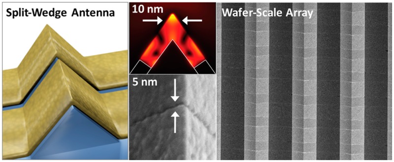
We present a novel plasmonic antenna structure, a split-wedge antenna, created by splitting an ultrasharp metallic wedge with a nanogap perpendicular to its apex. The nanogap can tightly confine gap plasmons and boost the local optical field intensity in and around these opposing metallic wedge tips. This three-dimensional split-wedge antenna integrates the key features of nanogaps and sharp tips, i.e., tight field confinement and three-dimensional nanofocusing, respectively, into a single platform. We fabricate split-wedge antennas with gaps that are as small as 1 nm in width at the wafer scale by combining silicon V-grooves with template stripping and atomic layer lithography. Computer simulations show that the field enhancement and confinement are stronger at the tip–gap interface compared to what standalone tips or nanogaps produce, with electric field amplitude enhancement factors exceeding 50 when near-infrared light is focused on the tip–gap geometry. The resulting nanometric hotspot volume is on the order of λ3/106. Experimentally, Raman enhancement factors exceeding 107 are observed from a 2 nm gap split-wedge antenna, demonstrating its potential for sensing and spectroscopy applications.
Keywords: Optical antenna, surface-enhanced Raman scattering (SERS), template stripping, gap plasmon, atomic layer deposition, atomic layer lithography
Nanometer-scale gaps1−3 and sharp tips4−8 made with noble metals are key building blocks for plasmonic devices,9,10 heat-assisted magnetic recording systems,11 metamaterials,12,13 and optical antennas.8,14−16 Nanogaps can sustain electromagnetic modes known as gap plasmons and are capable of extreme nanoscale confinement2 and enhancement of optical fields. Strong resonances at optical frequencies have been experimentally observed even in single-digit nanometer gaps formed by various methods.2,3,17−22 Sharp metal tips, however, have a three-dimensional (3D) geometry for nanoscale probing and can also confine optical fields far below the diffraction limit and enhance local field intensity via plasmonic nanofocusing.23,24 For these reasons, sharp tips made with gold or silver have been used for near-field scanning optical microscopy (NSOM)8 and nonlinear optics.5 Unfortunately, it is extremely difficult to fabricate metallic nanotips with a radius of curvature smaller than around 5–10 nm. This limit and the fact that metals tend to repel optical fields means that nanotips alone, where the confinement is limited by the field decay length into a surrounding dielectric medium, cannot achieve field confinement on the order of 1 nm. Nanogaps, however, can be routinely fabricated on the single nanometer scale. Furthermore, since both sides of the nanogap repel the optical field and constrain it within the gap, the field is tightly concentrated. This can be achieved in a metal–insulator–metal (MIM) structure2 or a nanotip–gap–substrate4 arrangement as with certain scanning probe geometries. Thus, an important extension of these research efforts is to combine single-digit nanogaps with the nanofocusing effect and 3D geometry of nanotips.
While hybrid structures combining gap plasmons and tip-based nanofocusing have been demonstrated,25−27 the 3D integration of nanogaps and nanotips requires difficult and time-consuming fabrication such as using electron-beam lithography (EBL) in conjunction with focused-ion beam (FIB) milling or electron-beam-induced metal deposition,28 all of which are low-throughput serial processes with patterning resolution in metals of ∼10 nm. It is therefore desirable to manufacture these advanced optical antennas with higher throughput and reproducibility and with smaller gaps and sharper tips.
In this letter, we introduce a new antenna design, a split-wedge antenna, that combines ultrasharp metal wedges and single-digit nanometer gaps. Among the various fabrication schemes for making sharp metal wedges and tips, template stripping from anisotropically etched silicon molds has been effective.29,30 With this technique, standard photolithography and wet etching in KOH can mass-produce ultrasharp metallic wedges (tip radius of curvature ∼10 nm) over an entire wafer. To manufacture nanometric gaps in metal films, many groups have used schemes such as thin-film deposition,2 electromigration,3 or electron-beam lithography.19 A process called atomic layer lithography was also developed by some of the authors to create nanogaps in metallic structures with wafer-scale throughput via atomic layer deposition (ALD).13,18,31−33 Because the critical lateral dimension is defined by ALD in this technique, vertical gaps as small as 1 nm that travel along the entire width of the wafer can be produced. Our desire to fabricate split-wedge antennas over an entire wafer thus naturally combines template stripping and atomic layer lithography. Here, following proof-of-concept fabrication with low-throughput FIB milling to design an initial set of devices, we show wafer-scale fabrication of split-wedge antenna arrays with single-digit nanogaps. These devices are characterized optically via surface-enhanced Raman spectroscopy (SERS), confirming that the field enhancement at the 3D tip–gap interface is stronger than that from either a standalone wedge tip or a planar nanogap.
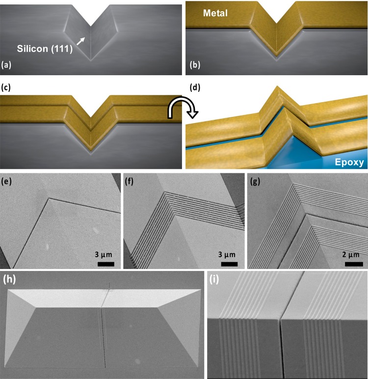
Our fabrication scheme for split-wedge antennas consists of two key steps: (1) silicon template fabrication and (2) gap formation in the metal deposited onto the template. The silicon template containing inverted wedges (V-shaped trenches with a divot angle of 70.5°) is created via crystal-orientation-dependent wet etching30,34−36 in a solution containing 30% potassium hydroxide (KOH) saturated with IPA at 80 °C (Figure 1a). After metal deposition and template stripping using an adhesive backing layer (NOA 61, Norland Products Inc.), sharp wedges can be created, as we previously showed.30 The taper angle of the wedge, 70.5°, is defined by intersecting (111) crystallographic planes in the V-groove silicon template. Previously researchers studied the effect of the taper angle on plasmonic nanofocusing and waveguiding.36−38 Fortunately, this 70.5° taper angle resulting from the anisotropic silicon etching leads to large enhancements in near-field fluorescence and Raman spectroscopy of single molecules36 and also nearly optimal figure-of-merit for wedge plasmon waveguiding.38 If shallower taper angles are desired for other applications, however, the silicon trench can be modified to reduce the taper angle.39−41 The measured radius of curvature of these template-stripped gold wedges is approximately 10 nm, consistent with previous reports.30,42 After metal deposition (Figure 1b), lithography is performed inside the nonplanar surfaces of the V-shaped trenches to create nanogaps that split the resulting metal wedges (Figure 1c). Different lithography techniques can be used for this purpose. For low-throughput prototyping over a small area, FIB lithography can be used to mill 50–100 nm wide gaps through a deposited metal film inside the V-shaped trenches. After stripping (Figure 1d), the structures shown in Figure 1d,e are formed. While not studied here, if desired, multiple grooves can be milled (Figure 1f) or the surface of the silicon template can be further engineered to create plasmonic reflectors38,43 or Bragg mirrors44,45 directly onto the template-stripped wedges (Figure 1g). The zoomed-out image in Figure 1h shows the entire device structure. Figure 1i shows a close-up of the structure in Figure 1g.
Figure 1.
Split-wedge antenna processing schematic and scanning electron micrographs. (a) A (100) silicon wafer is patterned with anisotropic KOH etching with Si3N4 etch mask, exposing slowly etching {111} facets. (b) A thin layer of gold film (typically 100–200 nm) is deposited. (c) For initial prototyping, FIB milling is used to create the gap. (d) An optical epoxy layer is applied and the structure is peeled from the V-groove template, exposing a metal wedge split by a nanogap. (e–i) SEMs of various split wedge structures.
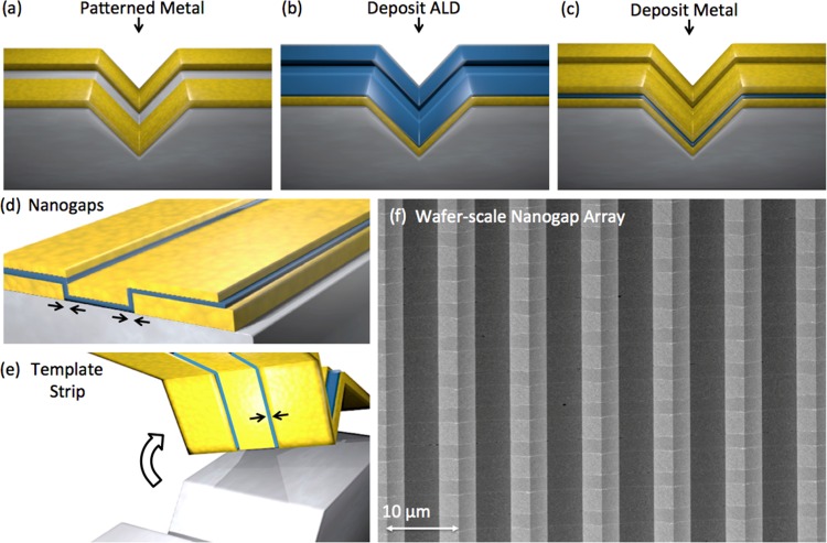
For wafer-scale fabrication of split-wedge antennas with ultrasmall (<10 nm) gaps, we employ atomic layer lithography (Figure 2) following the method developed by Chen and Oh.31−33 This method uses standard lithographic techniques such as photolithography, EBL, or FIB to initially pattern the metal film (Figure 2a) followed by adding thin ALD-grown oxide films (e.g., Al2O3) onto the sidewalls of the patterned metal (Figure 2b). Another metal deposition (Figure 2c) forms vertically oriented MIM nanogaps (Figure 2d) that are exposed via template stripping (Figure 2e). In this current work, fabrication of the split-wedge antennas required us to perform atomic layer lithography on the nonplanar surfaces of silicon V-grooves. To fabricate a large array shown in Figure 2f, we used photolithography to pattern a series of micrometer-wide stripes that are perpendicular to the wedge-axis orientation. The depth of the wedge used in this experiment is less than 5 μm, still allowing photolithography with the nonplanar surface. A two-step spin coating is used to improve the uniformity of spreading the resist inside and outside of the V-grooves. The resulting dense array of split-wedge antennas (SEM image in Figure 2f) demonstrates that 10 nm tip size and 5 nm gap size can be simultaneously obtained at the wafer scale. In this wafer-scale array, the base width of each wedge is 5 μm and the distance between adjacent wedge tips is 10 μm. The 5 nm gap size was defined by the thickness of the ALD-grown Al2O3 films. The width of each horizontal stripe is 1.8 μm. With further reduction in lithographic resolution using a stepper, it will be possible to densely pack sub-5 nm gap split-wedge antennas on submicron-scale grids. It should also be noted that the horizontal stripes are electrically isolated by the Al2O3 films and could be individually biased.
Figure 2.
Atomic layer lithography for wafer-scale production of split-wedge antenna arrays. (a) Photolithography, metal deposition, and lift-off are performed to pattern long horizontal metal stripes (1.8 μm width) into the silicon grooves. (b) After ALD growth of Al2O3 films and (c) a second metal evaporation, (d) nanogaps are naturally formed on the exposed sidewalls of each stripe. (e) Template stripping exposes these nanogaps. (f) Wafer-scale array of split-wedge antennas with 5 nm gaps.
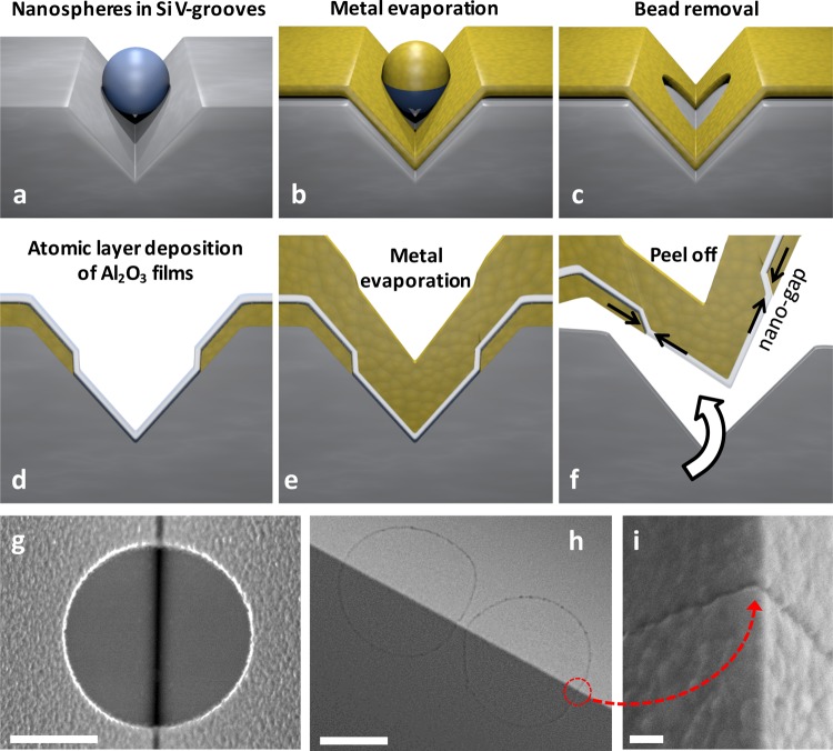
We also used microsphere or nanosphere lithography (NSL) techniques46 to create metal patterns inside V-groove templates without using photoresist (Figure 3). We first applied silica or polystyrene micro/nanospheres to the wedges by a drop-and-dry method (Figure 3a). The diameter of the spheres is chosen to be smaller than the trench depth such that the 1.83 μm diameter spheres can align inside the trenches. A dry etching in O2 plasma is then used to shrink the size of polystyrene spheres to obtain isolated spheres.47 The spheres on top of the surface are removed with a lift-off brush. Then a thin metal film (∼60 nm thick gold or silver) is evaporated onto the chip, creating areas shadowed by the spheres (Figure 3b). The spheres are then removed by gentle sonication leaving holes in metal film in the wedge mold (Figure 3c). After the patterns in metal are made in this way, a thin layer of Al2O3 is deposited conformally onto the surface and sidewall of the metal patterns via ALD (Figure 3d). The thickness of the ALD-grown Al2O3 film defines the width of the nanogap with Å-scale resolution. The ALD process was performed at 250 °C for depositing Al2O3 films (measured growth rate of 1.1 Å/cycle) on a gold substrate, and the temperature was reduced to 50 °C (growth rate of 1.0 Å/cycle) for depositing on a silver substrate to avoid unwanted oxidation. A second metal layer, thicker than the first metal layer, is deposited to completely cover the patterns (Figure 3e). Finally, optical adhesive (NOA61, Norland Products Inc.) is applied on the sample surface, cured under UV light for 15 min, followed by overnight baking on a hot plate at 55 °C. The multilayer structures, containing a layer of Al2O3 embedded in two metal films, are then stripped from the silicon V-groove mold (Figure 3f). SEM images show the initial metal pattern in the V-groove (Figure 3g), the template-stripped annular nanogaps on the wedge tip (Figure 3h), and a 5 nm wide nanogap on the wedge (Figure 3i).
Figure 3.
Atomic layer lithography for wafer-scale production of sub-10 nm gap split-wedge antennas. (a–f) Fabrication process of circular nanogap on wedges via nanosphere lithography, atomic layer lithography, and template stripping. Here micro/nanospheres inside the V-shaped trenches act as masks for metal deposition. (g) After metal evaporation, holes are created in metal films inside the trenches. Alumina is deposited by ALD to define sub-5 nm gaps. A second silver layer is deposited into the wedge. The entire stack is stripped by attaching it to a glass slide with a UV cured adhesive. (h) Two annular nanogaps formed on the wedge. (i) Zoomed in SEM images showing a 5 nm nanogap on silver wedge tip. The scale bars in (g) and (h) are 1 μm. The scale bar in (i) is 100 nm.
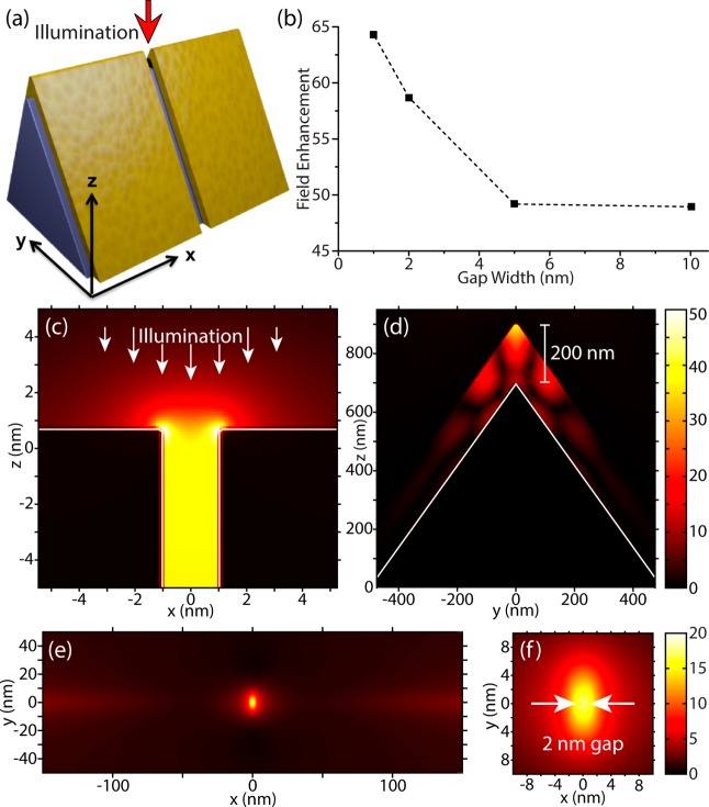
To illustrate the electric field enhancement distribution inside the nanogap on a wedge tip, we performed 3D finite-difference time-domain (FDTD) modeling for a metal wedge split by a nanogap of various widths (Figure 4). The incident light was polarized along the wedge axis, perpendicular to the nanogap. The 3D simulations demonstrate that smaller gaps tend to increase the field enhancement (Figure 4b) and that the field is tightly confined to within a few nanometers of the tip-gap interface (Figure 4c–f). Our split-wedge antennas act as a 3D bow-tie-type structure and combine the effects of wedge plasmons and gap plasmons into a single platform. The maximum electric field enhancement factor measured from a split-wedge antenna with a 2 nm gap is 58. Additionally, these simulations show that in the case of a 2 nm gap on a wedge tip with 10 nm radius, the plasmonic hotspot is approximately confined to an area of 9 nm by 14 nm, with the boundaries being defined by 1/e attenuation of the electric field. This corresponds to approximately a 1000× greater confinement of optical energy than a diffraction-limited spot. While resonant antenna operation was not investigated in this work, the addition of plasmonic Bragg mirrors or reflectors is expected to lead to even stronger field enhancements. Additionally, an internal illumination scheme may be used, where it is desirable to minimize or eliminate noise from propagating light while generating a hotspot that exists only within a small region.
Figure 4.
(a) Schematic of a beam of light illuminating a gap on a split-wedge antenna from above. The wedge tip has a 10 nm radius of curvature. (b–f) Results calculated via 3D FDTD modeling of electric field enhancement from nanogaps on a metal wedge illuminated from above by a focused Gaussian beam as in (a). In (b), the field enhancements at the tip–gap interface are plotted as a function of gap width, demonstrating increased field enhancement as the gap width decreases. (c) Electric field distribution in the x–z plane for a 2 nm gap. The region of strongest field enhancement is confined to within 2 nm of the tip–gap interface. (d) Electric field distribution inside the center of the nanogap. The electric field is strongest at the tip and decreases further down the wedge facet. (e,f) Electric field distribution in the x–y plane 1 nm above the tip. These field maps were used to calculate the volume of the hotspot to be 66 nm3 in the region outside the gap, with the volume boundary defined as the points of 1/e field extinction. (c) and (d) are plotted on the same amplitude scale, as are (e) and (f).
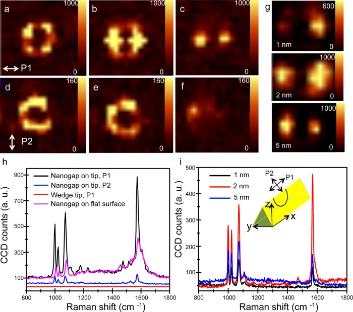
To experimentally demonstrate the intense optical near-fields of split-wedge antennas, we fabricated structures with single-digit nanometer gaps (widths of 1, 2, and 5 nm) and performed Raman spectroscopy after coating the silver surfaces with Raman-active molecules of interest. For this purpose, the circular gap structure shown in Figure 3i is convenient because a given device can possess gaps both perpendicular and parallel to the wedge axis to provide comparison measurements. The Al2O3 layer sandwiched between two layers of metal film can be partially removed via wet etching in buffered oxide etchant (BOE; HF/H2O = 1:10) to allow the molecules to attach recessed in the gap where the field is presumably more intense. After partially removing the Al2O3 in the gap in this way, the samples are incubated in 2 mM benzenethiol (BZT) in ethanol for 24 h to form a self-assembled monolayer on the exposed surfaces and inside gaps. The samples are then rinsed with ethanol spraying for 2 min to remove any excess BZT molecules. BZT is chosen because it has been extensively characterized as an efficient Raman scatterer by many groups.18 With a scanning confocal Raman microscope (WITec), surface-enhanced Raman scattering is imaged in the XY plane at different Z heights on the 3D split-wedge antenna structure. A 514.5 nm argon-ion laser is focused to a diffraction-limited spot by an objective lens (NA = 0.9) and scanned across the silver wedge by mounting the sample on an XYZ piezo stage as illustrated in Figure 5i inset. The scattered Raman signals are then collected with the same objective lens and measured by a spectrometer.
Figure 5.
Raman intensity images on XY plane at multiple Z positions (from the bottom of the circular nanogap to the wedge tip antenna) in 5 nm split-wedge antennas with laser polarized perpendicular (P1) to the nanogap (a–c) and parallel (P2) to the nanogap (d–f). The excitation laser wavelength is 514.5 nm. Similarly, Raman intensity images on XY plane at the tip of the split-wedge antennas with 752.5 nm laser polarized perpendicular to the nanogap with 1, 2, and 5 nm gap size are shown in (g). In (a)–(g), the wedge axis is along P1. The schematic of laser polarization to the direction of nanogap on the split-wedge antennas is shown as an inset in (i). The intensity images from (a)–(g) are generated by integration of the BZT aromatic ring breathing mode centered with 30 cm–1 spectral width. (h) Raman spectra at 5 nm split-wedge antennas, wedge tip only, and nanogap on flat surfaces, with light polarization P1 and P2. (i) Raman spectra of the split-wedge antennas from (g).
In the split-wedge antenna structures, the measured Raman intensity is strongly polarization-dependent. Figure 5a–c shows the Raman images collected at different Z positions (500 nm per step, from the bottom of the wedge to the tip of the wedge) in horizontal planes across the wedge and with the laser polarized perpendicular (P1) to the nanogaps. The gap plasmons, which are responsible for the majority of the field enhancement, can only be excited when the polarization of the incident laser beam is perpendicular to the gap, i.e., transverse magnetic (TM) polarization. For each scan plane, we can observe the 3D structures showing hotspots at different positions on the split-wedge antennas when the light is polarized perpendicular to the gap. The Raman scattering intensity at the nanogap on wedge tip with P1 polarized light is about 10 times stronger than with polarization along the gap (P2) (Figure 5d–f). We could still observe enhanced Raman signals with laser polarization parallel to the gap, likely due to the residual roughness of nanogap sidewalls (on the order of 1 nm) and lightning-rod effects from the sharp wedge tip. The Raman scattering spectra are shown in Figure 5h, where we compared the spectra at different polarizations from areas on the wedge tip that contained the nanogaps and areas on the wedge tip that did not contain any gaps. An enhancement factor of about 104 was obtained from placing 5 nm nanogaps on a silver wedge tip, in comparison to the Raman scattering of BZT coated on a flat silver surface. The enhancement factor is also 5 times higher compared with SERS from a nanogap on flat silver surface.
Though the structure is not designed to have a resonance at 514.5 nm, we observed enhanced Raman scattering from nanogaps on wedge tips. To check the wavelength dependence of the enhancement, the nanogap-on-wedge structures were also tested with a 752.5 nm laser. The Raman intensity images and spectra are shown in Figure 5g,i. As before, strong Raman scattering is observed from the nanogap structures. While FDTD simulations predict increasing field enhancements as the gap size shrinks from 5 to 1 nm, in our experiments the measured Raman signal intensity increases as the gap size changes from 5 to 2 nm, and then decreases as the gap size changes from 2 to 1 nm. Possible reasons for this discrepancy include surface roughness, variations in the gap size at 1 nm level, and the size of BZT molecule (0.6 nm),44 which is comparable to the width of the 1 nm gap, leading to steric hindrance effects. A more rigorous analysis of the dependence of field enhancements on gap size is beyond the scope of this work, but it is clear that the intensity of the Raman signals increases as the gap size is pushed into the single-digit nanometer regime.
While precise quantification of the Raman enhancement factor (EF) in a split-wedge antenna is not trivial because of its 3D geometry and nonuniform field distribution around the tip–gap interface, we use the following equation to estimate the field enhancement factor:
where EFgapSERS is the enhancement factor of Raman intensity in the tip–gap interface. We measured the Raman scattering from neat BZT (thiophenol, ≥99%, Sigma-Aldrich) in a quartz cuvette with 1 mm path length as a reference. IgapSERS and Ivol are Raman intensities of the in-plane ring breathing mode at 1072 cm–1 from BZT coated on the silver surface of nanogap sample and from the neat liquid BZT sample, respectively. Nvol is the number of BZT molecules in the laser focus volume in the pure liquid BZT. Nsurf is the number of BZT molecules in the laser spot area on the metal surface by adding the area inside the nanogaps for calculating averaged EF or the number of molecules in the area inside the nanogaps for calculating local EF, respectively. The packing density of BZT on a silver surface is assumed to be 6.8 × 10¹⁴ molecules/cm2 based on the literature.48 The averaged Raman EF is calculated by considering the metal surface area defined by the confocal spot size of the lens at the excitation laser wavelength. The confocal spot area plus the exposed metal area within the nanogaps is used to calculate Nsurf. The local EF calculation considers only the molecules inside the nanogap within the focused laser beam spot. For the 2 nm gap split–wedge antenna structure, we assume that the depth of the gap after BOE etching of Al2O3 film is also 2 nm. The radius of the tip measured by SEM is 10 nm, which according to our simulation data suggests the plasmonic hotspot is approximately 9 nm by 14 nm in size. In both cases, Igap and Ivol are measured by subtracting background CCD counts at 900 cm–1 from the CCD counts of the scattering band of interest.
For 2 nm gaps on a wedge, the measured average Raman enhancement factor over the full laser spot size was about 104, suggesting that the local enhancement factor can be as large as 107. This is also in line with our FDTD calculations, which predicts field enhancement of 58, and thus |E|4 on the order of 107. Our Raman characterization confirms that split-wedge antennas with small nanogaps can convert incident light into localized near-field hotspots. While precise tuning and optimizing resonances in this 3D structure is possible, it would require extensive parametric 3D simulations and a series of nanofabrication with different resonator schemes. This will be the focus of future work.
In summary, we have presented the design for split-wedge antennas and different fabrication options for realizing this unique 3D nanostructure. In particular, we have combined template stripping, which can mass-produce ultrasharp metallic wedges, with atomic layer lithography, which can insert single-digit-nanometer gaps to split those wedges, to create gaps as small as 1 nm alongside an ultrasharp wedge with the tip radius of 10 nm. Because both tips and gaps act to localize and boost optical fields, this antenna structure shows great potential for extreme plasmonic field confinement, which is demonstrated by SERS experiments. The antenna design and high-throughput atomic layer lithography scheme along with the addition of Bragg mirrors presented in this work can provide a new route for optical antennas, nonlinear optics,5 and near-field transducers.11 Furthermore, since atomic layer lithography can create long nanogaps that travel along the entire width of a chip, it is straightforward to split metallic wedges into electrode arrays that can be biased individually. Such structures, as shown in Figure 2f, will enable high-throughput experiments for electron tunneling,20,49 electroluminescence,50,51 photon upconversion,52 particle trapping,53−55 electrochemical plasmonic sensing,56 and hot-carrier effects57 in the presence of nanofocused fields at the tip.
Acknowledgments
This research was supported by the Office of Naval Research Young Investigator Program (to X.S.C., N.C.L. and S.-H.O.), the National Science Foundation (CMMI No. 1363334 for D.J.K. and S.-H.O.; ECCS No. 1610333 for S.-H.O.; CAREER Award No. 1552642 for N.C.L.; NSF Graduate Research Fellowship for D.J.K.), Seagate Technology (MINT grant for S.-H.O.), and the MnDrive Initiative from the State of Minnesota (to D.J.K. and S.-H.O.). X.S.C. acknowledges support from the 3M Science and Technology Fellowship and the University of Minnesota Doctoral Dissertation Fellowship. P.N. utilized funding from the U.S. Department of Energy (DE-FG02-06ER46348). D.J.N. acknowledges a grant (339905, QuaDoPS Advanced Grant) from the European Research Council under the European Union’s Seventh Framework Programme (FP/2007-2013). The authors also acknowledge the Minnesota Supercomputing Institute at the University of Minnesota for providing the resources necessary to carry out the FDTD calculations.
The authors declare no competing financial interest.
References
- Xu H.; Käll M. Phys. Rev. Lett. 2002, 89, 246802. 10.1103/PhysRevLett.89.246802. [DOI] [PubMed] [Google Scholar]
- Miyazaki H. T.; Kurokawa Y. Phys. Rev. Lett. 2006, 96, 097401. 10.1103/PhysRevLett.96.097401. [DOI] [PubMed] [Google Scholar]
- Ward D. R.; Grady N. K.; Levin C. S.; Halas N. J.; Wu Y.; Nordlander P.; Natelson D. Nano Lett. 2007, 7, 1396–1400. 10.1021/nl070625w. [DOI] [PubMed] [Google Scholar]
- Stöckle R. M.; Suh Y. D.; Deckert V.; Zenobi R. Chem. Phys. Lett. 2000, 318, 131–136. 10.1016/S0009-2614(99)01451-7. [DOI] [Google Scholar]
- Bouhelier A.; Beversluis M.; Hartschuh A.; Novotny L. Phys. Rev. Lett. 2003, 90, 013903. 10.1103/PhysRevLett.90.013903. [DOI] [PubMed] [Google Scholar]
- Ropers C.; Neacsu C. C.; Elsaesser T.; Albrecht M.; Raschke M. B.; Lienau C. Nano Lett. 2007, 7, 2784–2788. 10.1021/nl071340m. [DOI] [PubMed] [Google Scholar]
- Verhagen E.; Polman A.; Kuipers L. K. Opt. Express 2008, 16, 45–57. 10.1364/OE.16.000045. [DOI] [PubMed] [Google Scholar]
- Novotny L.; van Hulst N. F. Nat. Photonics 2011, 5, 83–90. 10.1038/nphoton.2010.237. [DOI] [Google Scholar]
- Halas N. J. Nano Lett. 2010, 10, 3816–3822. 10.1021/nl1032342. [DOI] [PubMed] [Google Scholar]
- Bozhevolnyi S. I.; Volkov V. S.; Devaux E.; Laluet J.-Y.; Ebbesen T. W. Nature 2006, 440, 508–511. 10.1038/nature04594. [DOI] [PubMed] [Google Scholar]
- Challener W. A.; Peng C.; Itagi A. V.; Karns D.; Peng W.; Peng Y.; Yang X.; Zhu X.; Gokemeijer N. J.; Hsia Y. T.; Ju G.; Rottmayer R. E.; Seigler M. A.; Gage E. C. Nat. Photonics 2009, 3, 220–224. 10.1038/nphoton.2009.26. [DOI] [Google Scholar]
- Burgos S. P.; de Waele R.; Polman A.; Atwater H. A. Nat. Mater. 2010, 9, 407–412. 10.1038/nmat2747. [DOI] [PubMed] [Google Scholar]
- Yoo D.; Nguyen N.-C.; Martín-Moreno L.; Mohr D. A.; Carretero-Palacios S.; Shaver J.; Peraire J.; Ebbesen T. W.; Oh S.-H. Nano Lett. 2016, 16, 2040–2046. 10.1021/acs.nanolett.6b00024. [DOI] [PMC free article] [PubMed] [Google Scholar]
- Bharadwaj P.; Deutsch B.; Novotny L. Adv. Opt. Photonics 2009, 1, 438–483. 10.1364/AOP.1.000438. [DOI] [Google Scholar]
- Giannini V.; Francescato Y.; Amrania H.; Phillips C. C.; Maier S. A. Nano Lett. 2011, 11, 2835–2840. 10.1021/nl201207n. [DOI] [PubMed] [Google Scholar]
- Brown L. V.; Yang X.; Zhao K.; Zheng B. Y.; Nordlander P.; Halas N. J. Nano Lett. 2015, 15, 1272–1280. 10.1021/nl504455s. [DOI] [PubMed] [Google Scholar]
- Wang H.; Levin C. S.; Halas N. J. J. Am. Chem. Soc. 2005, 127, 14992–14993. 10.1021/ja055633y. [DOI] [PubMed] [Google Scholar]
- Im H.; Bantz K. C.; Lindquist N. C.; Haynes C. L.; Oh S.-H. Nano Lett. 2010, 10, 2231–2236. 10.1021/nl1012085. [DOI] [PubMed] [Google Scholar]
- Koh A. L.; Fernandez-Dominguez A. I.; McComb D. W.; Maier S. A.; Yang J. K. W. Nano Lett. 2011, 11, 1323–1330. 10.1021/nl104410t. [DOI] [PubMed] [Google Scholar]
- Halas N. J.; Lal S.; Chang W.-S.; Link S.; Nordlander P. Chem. Rev. 2011, 111, 3913–3961. 10.1021/cr200061k. [DOI] [PubMed] [Google Scholar]
- Ciracì C.; Hill R. T.; Mock J. J.; Urzhumov Y.; Fernandez-Dominguez A. I.; Maier S. A.; Pendry J. B.; Chilkoti A.; Smith D. R. Science 2012, 337, 1072–1074. 10.1126/science.1224823. [DOI] [PMC free article] [PubMed] [Google Scholar]
- Lassiter J. B.; Chen X.; Liu X.; Ciracì C.; Hoang T. B.; Larouche S.; Oh S.-H.; Mikkelsen M. H.; Smith D. R. ACS Photonics 2014, 1, 1212–1217. 10.1021/ph500276v. [DOI] [Google Scholar]
- Babadjanyan A.; Margaryan N.; Nerkararyan K. V. J. Appl. Phys. 2000, 87, 3785–3788. 10.1063/1.372414. [DOI] [Google Scholar]
- Stockman M. I. Phys. Rev. Lett. 2004, 93, 137404. 10.1103/PhysRevLett.93.137404. [DOI] [PubMed] [Google Scholar]
- Choi H.; Pile D. F. P.; Nam S.; Bartal G.; Zhang X. Opt. Express 2009, 17, 7519–7524. 10.1364/OE.17.007519. [DOI] [PubMed] [Google Scholar]
- Choo H.; Kim M.-K.; Staffaroni M.; Seok T. J.; Bokor J.; Cabrini S.; Schuck P. J.; Wu M. C.; Yablonovitch E. Nat. Photonics 2012, 6, 838–844. 10.1038/nphoton.2012.277. [DOI] [Google Scholar]
- Suh J. Y.; Huntington M. D.; Kim C. H.; Zhou W.; Wasielewski M. R.; Odom T. W. Nano Lett. 2012, 12, 269–274. 10.1021/nl2034915. [DOI] [PMC free article] [PubMed] [Google Scholar]
- De Angelis F.; Gentile F.; Mecarini F.; Das G.; Moretti M.; Candeloro P.; Coluccio M.; Cojoc G.; Accardo A.; Liberale C.; Zaccaria R. P.; Perozziello G.; Tirinato L.; Toma A.; Cuda G.; Cingolani R.; Fabrizio E. D. Nat. Photonics 2011, 5, 682–687. 10.1038/nphoton.2011.222. [DOI] [Google Scholar]
- Sun C.-H.; Linn N. C.; Jiang P. Chem. Mater. 2007, 19, 4551–4556. 10.1021/cm0712319. [DOI] [Google Scholar]
- Nagpal P.; Lindquist N. C.; Oh S.-H.; Norris D. J. Science 2009, 325, 594–597. 10.1126/science.1174655. [DOI] [PubMed] [Google Scholar]
- Chen X.; Park H.-R.; Pelton M.; Piao X.; Lindquist N. C.; Im H.; Kim Y. J.; Ahn J. S.; Ahn K. J.; Park N.; Kim D.-S.; Oh S.-H. Nat. Commun. 2013, 4, 2361. 10.1038/ncomms3361. [DOI] [PubMed] [Google Scholar]
- Chen X.; Park H.-R.; Lindquist N. C.; Shaver J.; Pelton M.; Oh S.-H. Sci. Rep. 2014, 4, 6722. 10.1038/srep06722. [DOI] [PMC free article] [PubMed] [Google Scholar]
- Chen X.; Ciracì C.; Smith D. R.; Oh S.-H. Nano Lett. 2015, 15, 107–113. 10.1021/nl503126s. [DOI] [PubMed] [Google Scholar]
- Boltasseva A.; Volkov V. S.; Nielsen R. B.; Moreno E.; Rodrigo S. G.; Bozhevolnyi S. I. Opt. Express 2008, 16, 5252–5260. 10.1364/OE.16.005252. [DOI] [PubMed] [Google Scholar]
- Yang J.-C.; Gao H.; Suh J. Y.; Zhou W.; Lee M. H.; Odom T. W. Nano Lett. 2010, 10, 3173–3178. 10.1021/nl102078j. [DOI] [PMC free article] [PubMed] [Google Scholar]
- Johnson T. W.; Lapin Z. J.; Beams R.; Lindquist N. C.; Rodrigo S. G.; Novotny L.; Oh S.-H. ACS Nano 2012, 6, 9168–9174. 10.1021/nn303496g. [DOI] [PubMed] [Google Scholar]
- Moreno E.; Rodrigo S. G.; Bozhevolnyi S. I.; Martín-Moreno L.; García-Vidal F. J. Phys. Rev. Lett. 2008, 100, 023901. 10.1103/PhysRevLett.100.023901. [DOI] [PubMed] [Google Scholar]
- Kress S. J. P.; Antolinez F. V.; Richner P.; Jayanti S. V.; Kim D. K.; Prins F.; Riedinger A.; Fischer M. P. C.; Meyer S.; McPeak K. M.; Poulikakos D.; Norris D. J. Nano Lett. 2015, 15, 6267–6275. 10.1021/acs.nanolett.5b03051. [DOI] [PMC free article] [PubMed] [Google Scholar]
- Fernandez-Cuesta I.; Nielsen R. B.; Boltasseva A.; Borrisé X.; Pérez-Murano F.; Kristensen A. J. Vac. Sci. Technol. B 2007, 25, 2649–2653. 10.1116/1.2779041. [DOI] [Google Scholar]
- Im H.; Oh S.-H. Small 2014, 10, 680–684. 10.1002/smll.201301475. [DOI] [PubMed] [Google Scholar]
- Johnson T. W.; Klemme D. J.; Oh S.-H. ACS Appl. Mater. Interfaces 2016, 8, 13624–13629. 10.1021/acsami.6b01286. [DOI] [PubMed] [Google Scholar]
- Lindquist N. C.; Nagpal P.; Lesuffleur A.; Norris D. J.; Oh S.-H. Nano Lett. 2010, 10, 1369–1373. 10.1021/nl904294u. [DOI] [PubMed] [Google Scholar]
- Olson S. A. O.; Mohr D. A.; Shaver J.; Johnson T. W.; Oh S.-H. ACS Photonics 2016, 3, 1202–1207. 10.1021/acsphotonics.6b00091. [DOI] [Google Scholar]
- Lindquist N. C.; Lesuffleur A.; Oh S.-H. Phys. Rev. B: Condens. Matter Mater. Phys. 2007, 76, 155109. 10.1103/PhysRevB.76.155109. [DOI] [Google Scholar]
- Gordon R.; Marthandam P. Opt. Express 2007, 15, 12995–13002. 10.1364/OE.15.012995. [DOI] [PubMed] [Google Scholar]
- Haynes C. L.; Van Duyne R. P. J. Phys. Chem. B 2001, 105, 5599–5611. 10.1021/jp010657m. [DOI] [Google Scholar]
- Lee S. H.; Bantz K. C.; Lindquist N. C.; Oh S.-H.; Haynes C. L. Langmuir 2009, 25, 13685–13693. 10.1021/la9020614. [DOI] [PubMed] [Google Scholar]
- Whelan C. M.; Smyth M. R.; Barnes C. J. Langmuir 1999, 15, 116–126. 10.1021/la9806202. [DOI] [Google Scholar]
- Marinica D. C.; Zapata M.; Nordlander P.; Kazansky A. K.; Echenique P. M.; Aizpurua J.; Borisov A. G. Sci. Adv. 2015, 1, e1501095. 10.1126/sciadv.1501095. [DOI] [PMC free article] [PubMed] [Google Scholar]
- Lambe J.; McCarthy S. Phys. Rev. Lett. 1976, 37, 923–925. 10.1103/PhysRevLett.37.923. [DOI] [Google Scholar]
- Parzefall M.; Bharadwaj P.; Jain A.; Taniguchi T.; Watanabe K.; Novotny L. Nat. Nanotechnol. 2015, 10, 1058–1063. 10.1038/nnano.2015.203. [DOI] [PubMed] [Google Scholar]
- Sun Q.-C.; Mundoor H.; Ribot J. C.; Singh V.; Smalyukh I. I.; Nagpal P. Nano Lett. 2013, 14, 101–106. 10.1021/nl403383w. [DOI] [PubMed] [Google Scholar]
- Juan M. L.; Gordon R.; Pang Y.; Eftekhari F.; Quidant R. Nat. Phys. 2009, 5, 915–919. 10.1038/nphys1422. [DOI] [Google Scholar]
- Barik A.; Chen X.; Oh S.-H. Nano Lett. 2016, 16, 6317–6324. 10.1021/acs.nanolett.6b02690. [DOI] [PubMed] [Google Scholar]
- Pang Y.; Gordon R. Nano Lett. 2012, 12, 402–406. 10.1021/nl203719v. [DOI] [PubMed] [Google Scholar]
- Dahlin A. B.; Dielacher B.; Rajendran P.; Sugihara K.; Sannomiya T.; Zenobi-Wong M.; Vörös J. Anal. Bioanal. Chem. 2012, 402, 1773–1784. 10.1007/s00216-011-5404-6. [DOI] [PubMed] [Google Scholar]
- Knight M. W.; Sobhani H.; Nordlander P.; Halas N. J. Science 2011, 332, 702–704. 10.1126/science.1203056. [DOI] [PubMed] [Google Scholar]


