Significance
The miniaturization of electronic components and the excessive heating produced by the increased power densities in these small devices has heightened the need for on-chip cooling solutions. This has prompted a search for materials with large thermoelectric power factor and thermal conductivity that could be integrated in active thermoelectric coolers. Here, we report record thermoelectric power factors achieved in graphene on hexagonal boron nitride devices, corresponding to more than doubling the highest reported room temperature bulk values. In these devices, the smooth and highly efficient gating between electron- and hole-doped sectors, which facilitates switching the polarity of the Seebeck coefficient, extends a distinct advantage for on-chip thermoelectric cooling applications. Based on these results, we propose an integrated graphene-based active on-chip cooler.
Keywords: graphene, Seebeck coefficient, thermoelectric power factor, electron–hole puddles, screened Coulomb scattering
Abstract
Fast and controllable cooling at nanoscales requires a combination of highly efficient passive cooling and active cooling. Although passive cooling in graphene-based devices is quite effective due to graphene’s extraordinary heat conduction, active cooling has not been considered feasible due to graphene’s low thermoelectric power factor. Here, we show that the thermoelectric performance of graphene can be significantly improved by using hexagonal boron nitride (hBN) substrates instead of SiO2. We find the room temperature efficiency of active cooling in the device, as gauged by the power factor times temperature, reaches values as high as 10.35 W⋅m−1⋅K−1, corresponding to more than doubling the highest reported room temperature bulk power factors, 5 W⋅m−1⋅K−1, in YbAl3, and quadrupling the best 2D power factor, 2.5 W⋅m−1⋅K−1, in MoS2. We further show that the Seebeck coefficient provides a direct measure of substrate-induced random potential fluctuations and that their significant reduction for hBN substrates enables fast gate-controlled switching of the Seebeck coefficient polarity for applications in integrated active cooling devices.
As the size of the electronic components shrinks, larger power densities are generated, resulting in local hot spots. The small size of these hot spots and their inaccessibility make it difficult to maintain a low and safe operating temperature (1). Solid-state integrated active thermoelectric coolers could solve the long-lasting electronic cooling problem (2, 3). These coolers are designed to actively pump heat in its natural flow direction, from the hot spots generated on the chip to the colder ambient reservoir. In this mode of operation, active cooling assists passive cooling, which is different from the refrigeration mode where passive and active cooling oppose each other (4). In passive cooling, heat is transported via the phonon channel, and the heat flux is set by the thermal conductance of the cooler. In contrast, active cooling uses the Peltier cooling to pump heat via the electronic channel and can be controlled and tuned with applied current. The performance of Peltier cooling is a function of the thermoelectric power factor, , where is the electrical conductivity and S is the Seebeck coefficient. In this manuscript, we also use the notation of PFT, referring to PF times temperature T, which has a more convenient unit of watts per meter kelvin, the same as thermal conductivity. Unlike common thermoelectric applications, where the ability of a material to efficiently produce thermoelectric power is measured by its dimensionless figure of merit, ( is the thermal conductivity), thermoelectric cooling does not require low thermal conductivity. In fact, both the power factor and the thermal conductivity should be large. Although there is no theoretical limit on PF, the interplay between the Seebeck coefficient and the electrical conductivity in highly doped bulk semiconductors, has so far prevented the realization of very large thermoelectric power factors (5–7).
Single-layer graphene possesses extraordinary electronic and thermal properties (8–12). In particular, its high mobility, which due to the weak electron–phonon interaction persists up to room temperature, can be orders of magnitude higher than in other 2D thermoelectric materials, such as semiconducting transition metal dichalcogenides (13–16). Theoretical and experimental studies show that the Seebeck coefficient in graphene could reach values comparable to that in bulk semiconductors by decreasing the carrier density (17–23). The combination of graphene’s large mobility and competitive Seebeck coefficient result in large power factor and large active cooling. At the same time, graphene’s extremely large thermal conductivity also enables efficient passive cooling (12). Furthermore, the ability to control its carrier density by electrostatic gating rather than by chemical doping imparts to graphene an important advantage over bulk materials. Note that graphene owns low ZT because of its large thermal conductivity, and therefore it is only suitable for applications such as electronic cooling, which is the focus of this work.
As a purely 2D material, the electronic properties of graphene are strongly affected by its surroundings. Experiments demonstrate that the commonly used SiO2 substrate has surface charge states and impurities that cause Coulomb scattering that limits the mobility and introduce large potential fluctuations in G/SiO2 samples (24–26). The potential fluctuations induce electron–hole puddles (EHPs) in the vicinity of the charge-neutrality point (CNP) and prevent gating for lower carrier density (25). Depositing graphene on hexagonal boron nitride (hBN) substrates (G/hBN), which are relatively inert and free of surface charge traps, produces samples with smaller potential fluctuations and higher mobility than G/SiO2 (27–29). Here, we report on comparable measurements of the thermoelectric properties for G/hBN and G/SiO2 samples.
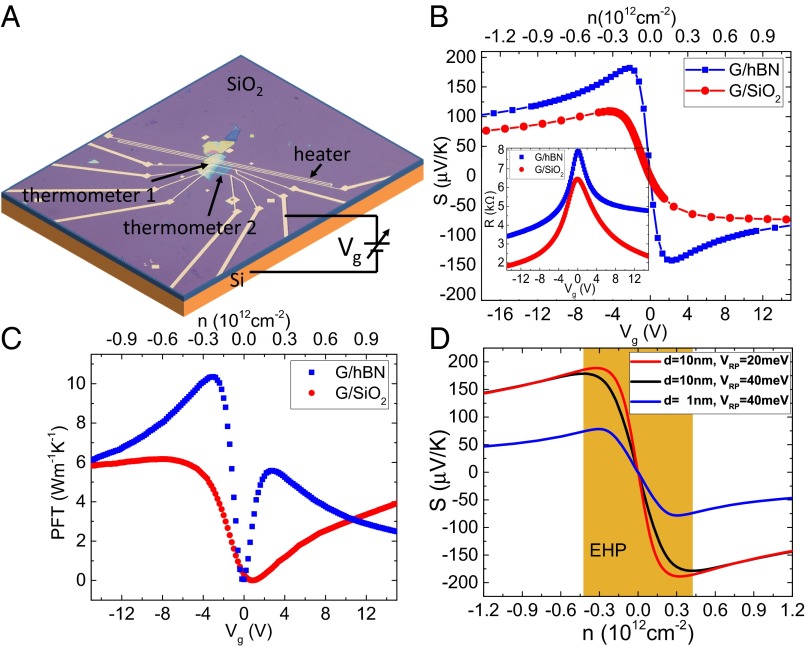
Fig. 1A shows a schematic of the apparatus for measuring the electrical and thermal transport properties (Supporting Information). Fig. 1B shows the gate voltage (Vg) dependence of the Seebeck coefficient, S(Vg), measured in G/hBN and G/SiO2 devices at 290 K. In both devices, S(Vg) is positive (negative) in the hole (electron)-doped sector. Its absolute value increases with decreased doping, reaches a peak value Sp at gate voltage Vp before vanishing at the CNP. We note that, in the G/hBN device, Sp = 182 μV/K and Vp = −2.2 V define a much sharper peak than in the G/SiO2 device, where Sp = 109 μV/K and Vp = −4.5 V. From the measured values of S and the conductivity of the devices, we calculate the value of as a function of carrier density shown in Fig. 1C (30). The PFT first increases with decreasing carrier density when far from CNP, and then after reaching a peak value, it drops rapidly to zero at the CNP. We find that the room temperature peak value of PFT in the G/hBN device, 10.35 W⋅m−1⋅K−1, is almost twice that in the G/SiO2 device, 6.16 W⋅m−1⋅K−1. This value is larger than the record value in bulk materials at room temperature reported for YbAl3 (∼5 W⋅m−1⋅K−1), and larger than the value at room temperature in 2D materials reported for MoS2 (∼2.5 W⋅m−1⋅K−1) and WSe2 (∼1.2 W⋅m−1⋅K−1) (30–33). As we discuss later, the PFT value increases with temperature, and because it is not yet saturated at room temperature, even larger PFT values are expected at higher temperatures.
Fig. 1.
Thermoelectric measurement of graphene at room temperature. (A) Optical micrograph of the graphene on hBN (G/hBN) device. (B) Measured Seebeck coefficient in G/hBN and G/SiO2 devices as a function of back gate at 290 K. (Inset) Measured resistance vs. Vg in both devices at 290 K. (C) Measured PFT in both samples as a function of back gate at 290 K. (D) Simulation of carrier density dependence of the Seebeck coefficient at 300 K using the screened Coulomb-scattering model for two values of the hBN thickness, d, and random potential fluctuations, VRP, induced by charge impurities (Supporting Information). The rectangular shadow corresponds to the EHP region in a sample with d = 10 nm and VRP = 40 meV.
We next use the linear Boltzmann equation in the relaxation time approximation to relate the Seebeck coefficient to the experimentally controlled quantities. Within this model, the response of the electrical and thermal current densities, j and jq, to the electric field, E, and temperature gradient, , are given by the following (17):
| [1] |
| [2] |
where , and
| [3] |
Here, , is the Fermi velocity, is the chemical potential, is the equilibrium Fermi–Dirac distribution function, and is the Boltzmann constant. The differential conductivity is , where is the density of states including the fourfold degeneracy of graphene, is the Fermi velocity (34), and is the relaxation time. The Seebeck coefficient is defined as , the electrical and thermal conductivity are and , respectively, and the Peltier coefficient is (17, 35). Importantly, we note that the Seebeck coefficient is controlled by the energy dependence of the conductivity.
In Fig. 1D, we show the calculated carrier density dependence of the Seebeck coefficient at 300 K in the presence of random potential fluctuations (RPFs) induced by charge impurities (Supporting Information). The calculation follows the model proposed in ref. 17 and, for simplicity, considers only the screened Coulomb scattering, which is known to be dominant in this system at low carrier densities (15, 17, 36–38). We note that the monotonic increase of S with decreasing carrier density peaks at the point where the Fermi energy enters the EHP region (17, 18). In this region (shadow area in Fig. 1D), both electrons and holes are present, but because they contribute oppositely to S, the value of S drops. Consequently, the narrower the energy range of the EHP region, the higher the peak value of S. There is, however, a limit to the magnitude of S that is set by the temperature. When kBT becomes comparable to the energy scale of the RPF, the temperature starts controlling the value of Sp. The effect of inserting the hBN spacer, typically d ∼ 10 nm, is to increase the distance from the charge impurities in the SiO2 substrate, which not only reduces the magnitude of the RPF in the graphene plane but also increases the electron–hole asymmetry resulting in a larger value of Sp (Supporting Information). Again, there is a limit to this improvement. For infinitely large separation, that is, no Coulomb scattering, thermally excited phonons become the dominant mechanism that limits the value of S. In the acoustic phonon-dominated regime, the Seebeck coefficient at room temperature is expected to be smaller than S = 100 μV/K (17).
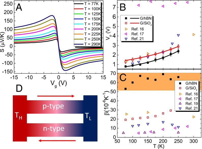
As discussed above, Vp marks the boundary of the EHP region, which depends on both the temperature and the extent of the RPF. In the high-temperature limit, this region is dominated by thermal excitations, whereas at low temperatures it is controlled by the energy scale of the RPF. Currently, most measurements of the EHP are carried out by scanning probe microscopy, which are typically performed at low temperatures and over a scanning range much smaller than the size of transport devices (28, 29, 39). Although the boundary of the EHP region can be estimated from the gate dependence of the resistivity (27), Vp provides a more direct measure of the EHP region. In Fig. 2A, showing the back-gate dependence of S in the temperature range of 77–290 K, we note that as the temperature decreases Sp moves closer to the CNP while at the same time its magnitude diminishes.
Fig. 2.
Temperature dependence of the Seebeck coefficient and EHP region. (A) Measured Seebeck coefficient in the G/hBN device as a function of back-gate voltage and temperature. (B) Temperature dependence of peak positions of the Seebeck coefficient (Vp) on the hole side for G/hBN (solid squares) and G/SiO2 (open squares) devices are shown together with the exponential fit discussed in the text (solid lines). (C) Slope of polarity-switching effect, , for both devices (solid squares for G/hBN and open squares for G/SiO2). Values of Vp and in G/SiO2 samples (open triangles) extracted from previous studies are also shown. (D) Sketch of the proposed graphene-based active cooling device with integrated n-type and p-type legs.
In the following discussion, we focus on the hole side because the peaks on this side are clearer in the G/SiO2 sample. The temperature dependence of Vp, shown in Fig. 2B for both samples, follows an exponential function, , where a, b, and are fitting parameters. The intercept at T = 0 provides access to the carrier density fluctuations (EHP region) and to the magnitude of the RPF. From the data in Fig. 2B, we find = 0.12 and 0.52 V for the G/hBN and G/SiO2 samples, respectively. This corresponds to carrier density fluctuations of 1.8 × 10¹⁰ and 7.6 × 1010 cm−2, and to RPF energy scales of 21.8 and 45.4 meV for the G/hBN and G/SiO2 samples, respectively. Both values are comparable to previous results measured by scanning tunneling microscopy at liquid-helium temperature (29). A comparison with the temperature dependence of Vp extracted from previous studies shows that the hBN substrates produce significantly narrower peaks in S(Vg) corresponding to the superior sample quality with a substantial reduction in the range of the RPF.
Unlike the case of the voltage drop in electrical transport measurements, which is insensitive to the sign of the carrier charge, the Seebeck voltage reverses its sign when switching from hole doping to electron doping. In the G/hBN sample, the polarity of Sp can be reversed with a relatively small gate voltage ∼2VP. We define as the slope of the polarity-switching effect: . A comparison of values in G/hBN and in G/SiO2 samples in both the present and earlier studies clearly shows that the switching efficiency is substantially enhanced in G/hBN (Fig. 2C).
The bipolar nature of graphene, which allows smooth gating between electron- and hole-doped sectors, together with the large values of , which facilitate switching the polarity of S, extend a distinct advantage for on-chip thermoelectric cooling applications. This can be seen in the thermoelectric active cooler design shown in Fig. 2D, which can pump heat from the hot end (TH) to the cold end (TL) in a controlled and fast manner using combined active and passive cooling effects. In this G/hBN-based device, the p–n legs are arranged thermally in parallel and electrically in series to maximize the active cooling (4). Its structure is readily realized with lithographically patterned gates because gating is more effective in 2D devices than in bulk devices where charge carriers will accumulate near the interface. Also, unlike the doping method, gating will not introduce extra charge-scattering centers. At the optimal value of the applied current, the active cooling power of the device is /2 (4). On the other hand, the passive cooling power is , where κ ∼ 600 W⋅m−1⋅K−1 is the thermal conductivity of graphene supported on a substrate at room temperature (12). For and , active cooling contributes an additional 10% over the passive cooling. At higher temperatures, as PFT increases and the thermal conductivity decreases, the contribution of active cooling further increases.
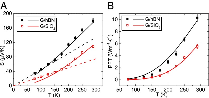
The temperature dependence S(T) at a fixed back-gate voltage for both samples is shown in Fig. 3A. The corresponding carrier density in G/hBN and G/SiO2 is −0.2 × 10¹² and −0.3 × 1012 cm−2, respectively. We note that, for both devices studied here, S(T) does not follow the linear dependence (dashed lines) expected from Mott’s equation (40). To understand this result, we must take into account the screened Coulomb scattering, which plays an important role in both samples. In the G/SiO2 sample, screened Coulomb scattering is the dominant mechanism as indicated by the linear dependence of the conductivity on carrier density (27, 41, 42). In the G/hBN samples, Coulomb scattering is also dominant at low carrier density, but at higher densities it crosses over to short-range impurity scattering (Supporting Information) (27). Therefore, to present a meaningful comparison between the two samples, we choose a carrier density smaller than the crossover point for the G/hBN sample. Using the screened Coulomb scattering model in the linear response theory to calculate S(T) and with only one fitting parameter (Supporting Information), we obtain the solid lines in Fig. 3A, which show good agreement with the measured quadratic T dependence of the S(T) curves (17). Similarly, the temperature dependence of the measured and calculated PFT are shown in Fig. 3B. In the calculation, inelastic electron–phonon interaction is not included because the screened Coulomb scattering is dominant in this temperature range as indicated by the energy scale of the RPF. However, electron–phonon scattering could become important when the temperature yields a kBT that is much higher than the energy of RPF as in the case for hBN-encapsulated graphene devices (43).
Fig. 3.
Temperature dependence of the Seebeck coefficient and PFT at fixed carrier density. (A) Measured Seebeck coefficient in G/hBN (, solid squares) and G/SiO2 (, open squares) devices are plotted together with the theoretical values (solid lines) calculated by using the screened Coulomb-scattering model discussed in the text. Dashed lines serve as guides to emphasize the nonlinear behavior. (B) Measured PFT (same density as in A; solid and open squares) from both devices are compared with theoretical values (solid lines).
In summary, we have shown that Sp in G/hBN device reaches twice the value measured in G/SiO2 device and its peak PFT value of 10.35 W⋅m−1⋅K−1 significantly exceeds previously reported records in both 2D and 3D thermoelectric materials. We demonstrate that the peak of the S(Vg) curves provides a direct measure of the RPF and substrate quality through the width of the EHP region. In particular, we find a fourfold reduction of the RPF in G/hBN, compared with G/SiO2 samples. We further show that the bipolar switching slope is significantly larger in the G/hBN devices, which makes it possible to integrate all-in-one graphene p-type and n-type devices. The study demonstrates the advantage of using graphene in thermoelectric applications especially in electronic cooling where large thermal conductivity (passive cooling) and large thermoelectric power factor (active cooling) are needed simultaneously.
Methods
Graphene on hBN samples are fabricated using the poly(methyl methacrylate) (PMMA)-based dry transfer method (44). hBN is exfoliated on a 300-nm SiO2/Si substrate. The hBN thickness is measured by atomic-force microscopy (AFM). Single-layer graphene is prepared on a PMMA membrane. It could be identified by optical microscopy through the color contrast and after the transfer by AFM and Raman measurements. In the case of G/SiO2, the graphene flake is directly exfoliated on the SiO2 surface. Electrodes on the graphene sample serve as voltage probes and thermometers measuring the local temperature at the two ends of graphene flake. A strip of gold wire next to the sample is used as a heater. Fig. 1A shows the optical micrograph of a typical sample. To induce a uniform temperature gradient across the sample, the size of the heater (400 μm) is much larger than the size of the graphene flake (typically 20 μm × 10 μm) and thermometers (40 μm). Thermometers and heater are defined by standard electron beam lithography. Cr/Au (3/45-nm) layers are deposited using electron beam evaporation. All of the samples are annealed in forming gas (H2/Ar) at 230 °C over 12 h to remove resist residue before measurements.
The temperature is measured through the four-probe resistance of the thermometers with resolution smaller than 0.01 K. By powering up the heater, a temperature gradient is generated along the sample (Fig. 1A). The thermally induced voltage is measured by the voltage probes at the two ends of the sample. The Seebeck coefficient is then calculated using the following: . is required to make the measurement in the linear response regime. All of the measurements are carried out in vacuum () over a temperature range of 77–300 K.
Associated Content.
Supporting Information includes the following: device characterization, Seebeck measurement, summary of recently reported PFT in 2D materials, nonlinear dependence on temperature, results from other G/hBN samples, thermal conductivity and thermoelectric figure of merit, and calculation details.
Device Characterization
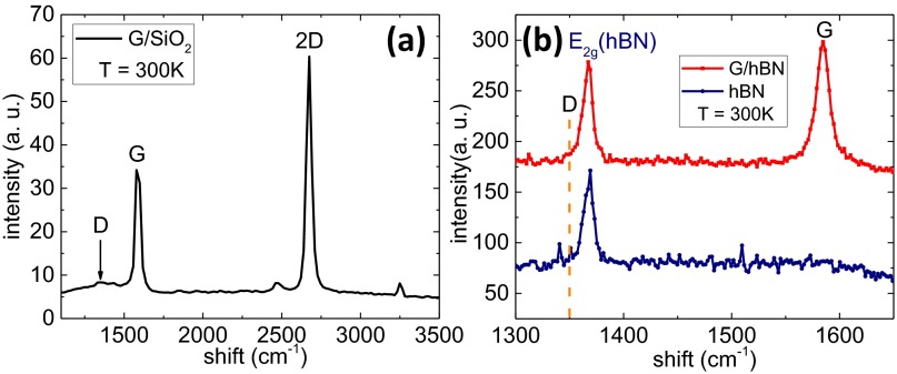
We measured three G/hBN samples (S1–S3; S1 is the one shown in the text) and one G/SiO2 sample. In Fig. S1, we show the Raman spectrum from the G/hBN sample S1 and the G/SiO2 sample. No distinct defect peak (D peak) in graphene could be observed in the G/SiO2 sample (Fig. S1A). For the G/hBN sample, the bulk hBN substrate will contribute a significantly large E2g peak (∼1,366 cm−1), which is close to the D peak (∼1,350 cm−1) of graphene (45). We use a high-resolution grating to scan the small window of interest. As shown in Fig. S1B, from the comparison, no distinct D peak could be observed, which indicates the high quality of the graphene flake.
Fig. S1.
Raman spectrum of G/hBN and G/SiO2 sample. (A) Raman curve of G/SiO2 sample at room temperature. (B) High-resolution Raman curve of G/hBN (red) and hBN (navy) at room temperature.
In the main text, we show the results from the G/hBN S1 and G/SiO2 samples with the highest mobility, 1.8 × 10⁴ and 1.2 × 104 cm2⋅V−1⋅s−1 on the hole side at 77 K, respectively. To calculate the carrier density, we adopt the parallel-plates capacitor model with 300 nm for the SiO2 thickness and the thickness d of the hBN layer determined by AFM. The dielectric constants of SiO2 and hBN are known. By measuring the resistance at different back-gate voltages, Vg, we determine the position of the charge-neutrality point (CNP carrier density n = 0), VD, which corresponds to the resistance peak. Using VD as the reference point for the CNP together with the parallel-plate capacitor model, we obtain for each sample, where C is the capacitance per unit area of the parallel-plates capacitor and e is the elementary charge.
Seebeck Measurement
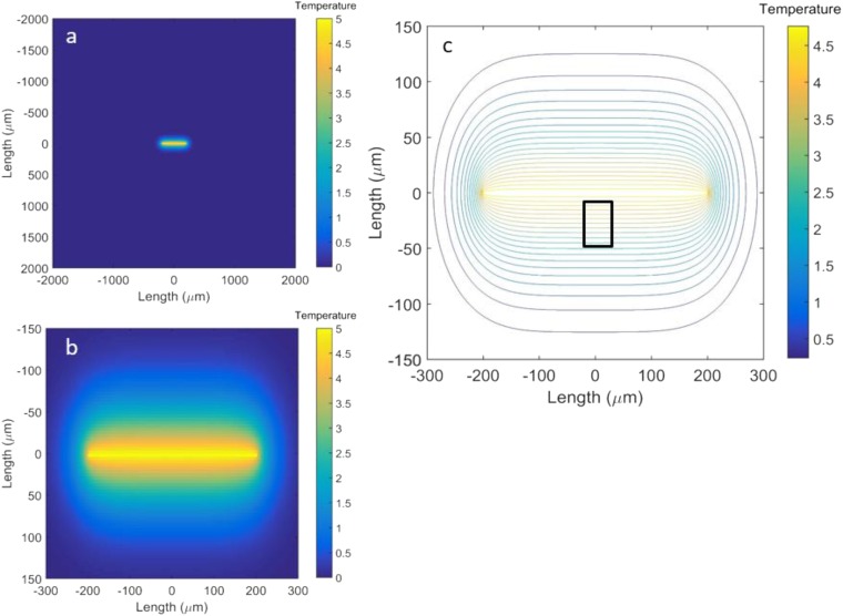
To minimize the systematic error caused by the nonuniform temperature distribution along the thermometer lines, the length of the heater (400 μm) is designed to be an order of magnitude longer than the thermometers (40 μm) and the graphene channel (typically 20 μm). Fig. S2 A and B shows the simulated temperature distribution in the device. Fig. S2C shows isotherms close to the heater. Because the size of the thermometers and the channel is only 1/10 of the size of the heater, one can see that the isotherms in this small region (as indicated) are actually straight lines running parallel to the heater. From the simulation, one can estimate that the systematic error introduced by the finite thermometer size is less than 0.1%.
Fig. S2.
Simulation of temperature distribution. (A) Temperature distribution in the device (4,000 μm × 4,000 μm). (B) Zoom-in view of A. The temperature of the 400-μm heater in the center is assumed to be uniform. (C) Isotherms in the vicinity of the heater. The rectangular box, 40 μm × 40 μm, indicates the area in which the thermometers and graphene channel are located.
Summary of Recently Reported PFT in 2D Material Devices
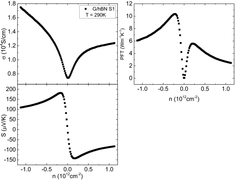
Comparing to other 2D material devices, the G/hBN device in this study shows much higher thermoelectric power factor times temperature (PFT) value at room temperature. Table S1 summarizes recently reported optimized PFT in 2D materials at room temperatures. Also, to make the comparison clear, Fig. S3 shows the carrier density dependence of the conductivity, the Seebeck coefficient, and the PFT of the G/hBN sample. Here, we note that, in the calculation of the PFT, the contact resistance is included. We are actually talking about PFT of the device rather than the material because the contact resistance could not be totally eliminated in real 2D devices.
Table S1.
Summary of recently reported PFT at room temperature in 2D materials
Fig. S3.
Carrier density dependence of conductivity, Seebeck coefficient, and PFT in G/hBN S1.
Nonlinear Temperature Dependence
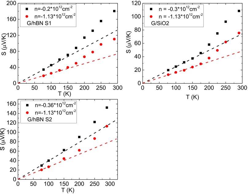
The nonlinearity of the measured T dependence of the Seebeck coefficient for both G/hBN and G/SiO2 samples with both low and high carrier density is shown in Fig. S4. Dashed lines are guides indicating the nonlinearity. All cases, high and low density in G/hBN and G/SiO2 samples, show deviations from a linear temperature dependence above a certain temperature (about 100 K).
Fig. S4.
Seebeck coefficient in three samples with different carrier densities vs. temperature.
Results from Other G/hBN Samples
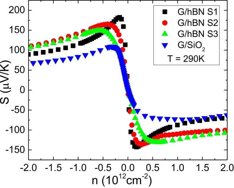
We have measured other G/hBN samples whose results are not shown in the main text. The Seebeck coefficient vs. hole and electron concentrations measured at room temperature (290 K) in these samples is shown below in Fig. S5.
Fig. S5.
Data from other G/hBN samples as well as for the samples shown in the text.
Samples G/hBN S1 (dhBN ∼ 10 nm) and G/SiO2 are shown in the main text. In G/hBN samples S2 (dhBN ∼ 21 nm) and S3 (dhBN ∼ 17 nm), the size of EHP region, as indicated by the position of Vp, is comparable to the G/SiO2 sample, but the measured Seebeck coefficient is larger than that in the G/SiO2 sample. This supports the assumption that by increasing the distance between graphene and the source of charge impurities the hBN spacer helps increase the Seebeck coefficient. Comparing the results from the three G/hBN samples, we note that the increase in Sp is directly correlated with the decrease in Vp. This result demonstrates that, by reducing the size of EHPs, one can improve the Seebeck coefficient further. The simulation discussed below shows that the Seebeck coefficient in G/hBN starts saturating when the hBN spacer is thicker than 10 nm.
Thermal Conductivity and Thermoelectric Figure of Merit
Thermal conductivity is related to the passive cooling of the device. For suspended single-layer graphene, previous Raman and electric measurements show extraordinarily high thermal conductivity, which is ∼1,500–5,000 W⋅m−1⋅K−1 (11, 46, 47). For practical application, graphene is supported by substrates like SiO2 or hBN. When graphene is supported by SiO2, the thermal conductivity is reduced to ∼600 W⋅m−1⋅K−1 (12). The reason is that, in supported graphene, the coupling between graphene and substrate will reduce the thermal conductivity of graphene. First, phonons could leak from graphene to the substrate. Second, phonons in graphene could be scattered by the substrate.
Another important parameter characterizing the thermoelectric performance of a material is the thermoelectric figure of merit (Z). It is usually expressed by multiplying temperature (T) as a unitless parameter , where S is the Seebeck coefficient, is the conductivity, and is the thermal conductivity. From the definition, ZT is proportional to the power factor and temperature but inversely proportional to thermal conductivity. However, ZT determines the potential of a material in the thermoelectric applications to power generation and refrigeration (30). For current study, the active cooler needs both the high thermoelectric power factor and high thermal conductivity.
Calculation Details
For screened Coulomb scattering, the energy dependence of the relaxation time is as follows:
| [S1] |
where is the scattering angle, and is the Fourier transform of a 2D Coulomb potential with dielectric constant . The 2D finite-temperature static random phase approximation screening function is , where is the irreducible finite-temperature polarizability function, is the DOS at Fermi level, and is the bare Coulomb interaction. For ,
where is Riemann’s ζ function and is the Fermi temperature. The Fermi velocity in graphene is taken as 1 × 10⁶ m/s. is taken as the average of the dielectric constants of the vacuum and the substrate, which is (1 + 4)/2 = 2.5. The fine-structure parameter is 0.85.
In the linear response approximation, the Seebeck coefficient and electrical conductivity are defined as follows:
| [S2] |
| [S3] |
where , is the Fermi velocity, is the chemical potential, is the equilibrium Fermi–Dirac distribution function, is the Boltzmann constant, is the density of states including the fourfold degeneracy of graphene, vF = 106 ms−1 is the Fermi velocity, and is the relaxation time. The Seebeck coefficient S is not sensitive to the magnitude of the electrical conductivity, but it is sensitive to its energy dependence. In the calculation of S, the integrand is taken within a Fermi window of [] centered at the Fermi energy .
Charge impurities generate random potential fluctuations (RPFs), which scatter the carriers. EHPs are the result from both thermal excitations and RPF. To simulate the effect of the RPF, a simplified model is adopted in which the RPF introduces local carrier density fluctuations in the graphene sample. The graphene channel is divided into small islands with uniform carrier density within each island. The carrier density fluctuates randomly between the islands with a distribution chosen to be flat within a certain density range corresponding to a uniform distribution of local potentials over an energy range [], where is the magnitude of the random potential fluctuations. The Seebeck coefficient of the entire sample is given by the average of the contribution from all of the islands weighted by the thermal conductivity and volume fraction of each. Because the thermal conductivity of graphene is dominated by phonons, the thermal conductivity of all of the islands is assumed to have the same value (48, 49). The total Seebeck coefficient is then given by averaging the Seebeck coefficients of all of the islands. The results of the simulation for two values of d and VRP are shown in Fig. 1D. Clearly, the distance between the graphene layer and the magnitude of the RPF are crucial parameters. Furthermore, as expected, the Seebeck coefficient calculated with larger VRP shows a lower and wider peak in a plot of S vs. n.
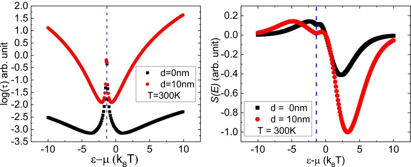
When inserting the hBN spacer between graphene and the SiO2 substrate, the Coulomb potential in the graphene plane is weakened. If the density of charge impurities is unchanged, the potential fluctuations will become smaller. At the same time, the slope of the lifetimes vs. energy increases, resulting in larger Seebeck coefficient values (40). Fig. S6 shows the energy dependence of relaxation time [] and normalized contribution [] at different energy () with n = 0.2 × 1012 cm−2, where and is a normalization parameter. The simulation demonstrates that, with larger d, stronger electron–hole asymmetry is expected in each island with uniform carrier density. The Seebeck coefficient is the summation of the contribution from hole and electron parts. Thus, the stronger asymmetry increases the Seebeck coefficient.
Fig. S6.
Comparison of energy dependence of relaxation time [τ(ε)] and electron–hole asymmetric contribution [S(E)] to Seebeck coefficient between d = 0 nm and d = 10 nm calculations with carrier density of . Dashed line gives the position of CNP.
To simulate the temperature dependence, we choose the carrier density to be outside the EHP region where the effect of the RPF could be neglected, as shown in Fig. 1D. From previous studies, there are many sources of the charge impurities. For SiO2 substrate, it has surface dangling bonds and trapped oxide charges (25). Studies show higher mobility in graphene on hBN substrate compared with that of graphene on SiO2, because it is free of dangling bonds and charge traps (27–29). Resist residue during the fabrication, like lithography, treatment in UV-ozone, and so on, will serve as another source of potential fluctuations. It also indicates that the atmospheric molecules (like H2O) trapped between flake and substrate or physisorbed on the flake surface will introduce extra charge impurities (25). Therefore, in the G/SiO2 sample, the charge impurities are near the SiO2 surface. Assuming the same distance, d, for all of the impurities, we find that, for d = 1.1 nm and , the simulation agrees with the experiment. From the definition of the Seebeck coefficient, S is not sensitive to the density of charge impurities. So d is the only parameter entering the calculation for the SiO2 sample. For the G/hBN sample, however, we must take into account two layers of impurities with one located at the SiO2/hBN interface and the other at the G/hBN interface. The simulation for the G/hBN device therefore uses two layers of charge impurities. The first layer on the SiO2 surface is at a distance from the graphene flake as measured by AFM. The second layer is on the G/hBN interface where is used. As shown in Fig. 3 of the main text, the experimental results are well matched by using and for the impurity density in layers 1 and 2, respectively. The actual density of charge impurities is not crucial, but what is important is the ratio between the densities of the charge impurities in these two layers, which is the only fitting parameter.
The deviations of the experimental data from the theoretical prediction can be attributed to several simplifications. First, all charge impurities are assumed to reside at the same distance from graphene layer. Second, other parameters that are known to depend on the details of the substrate, such as the Fermi velocity, were fixed to accepted values. Third, the model considers Coulomb scattering alone. Although in the regime studied here this is the dominant scattering mechanism, other weaker mechanisms that come into play such as the electron–phonon interactions or scattering from bulk and edge defects, have different energy and temperature dependences and may also contribute to the deviation.
Acknowledgments
M.Z. and J.D. acknowledge support from the Air Force Young Investigator Award (Grant FA9550-14-1-0316), E.Y.A. acknowledges support from Grant DOE-FG02-99ER45742, and J.D. acknowledges support from National Science Foundation Grant DMR 1207108.
Footnotes
The authors declare no conflict of interest.
This article contains supporting information online at www.pnas.org/lookup/suppl/doi:10.1073/pnas.1615913113/-/DCSupplemental.
References
- 1.Pop E, Sinha S, Goodson KE. Heat generation and transport in nanometer-scale transistors. Proc IEEE. 2006;94(8):1587–1601. [Google Scholar]
- 2.Snyder GJ, Toberer ES. Complex thermoelectric materials. Nat Mater. 2008;7(2):105–114. doi: 10.1038/nmat2090. [DOI] [PubMed] [Google Scholar]
- 3.Vaqueiro P, Powell AV. Recent developments in nanostructured materials for high-performance thermoelectrics. J Mater Chem. 2010;20(43):9577–9584. [Google Scholar]
- 4.Zebarjadi M. Electronic cooling using thermoelectric devices. Appl Phys Lett. 2015;106(20):203506. [Google Scholar]
- 5.Zebarjadi M, et al. Power factor enhancement by modulation doping in bulk nanocomposites. Nano Lett. 2011;11(6):2225–2230. doi: 10.1021/nl201206d. [DOI] [PubMed] [Google Scholar]
- 6.Zebarjadi M, Liao B, Esfarjani K, Dresselhaus M, Chen G. Enhancing the thermoelectric power factor by using invisible dopants. Adv Mater. 2013;25(11):1577–1582. doi: 10.1002/adma.201204802. [DOI] [PubMed] [Google Scholar]
- 7.Liang W, et al. Field-effect modulation of Seebeck coefficient in single PbSe nanowires. Nano Lett. 2009;9(4):1689–1693. doi: 10.1021/nl900377e. [DOI] [PubMed] [Google Scholar]
- 8.Geim AK, Novoselov KS. The rise of graphene. Nat Mater. 2007;6(3):183–191. doi: 10.1038/nmat1849. [DOI] [PubMed] [Google Scholar]
- 9.Novoselov KSA, et al. Two-dimensional gas of massless Dirac fermions in graphene. Nature. 2005;438(7065):197–200. doi: 10.1038/nature04233. [DOI] [PubMed] [Google Scholar]
- 10.Zhang Y, Tan YW, Stormer HL, Kim P. Experimental observation of the quantum Hall effect and Berry’s phase in graphene. Nature. 2005;438(7065):201–204. doi: 10.1038/nature04235. [DOI] [PubMed] [Google Scholar]
- 11.Balandin AA, et al. Superior thermal conductivity of single-layer graphene. Nano Lett. 2008;8(3):902–907. doi: 10.1021/nl0731872. [DOI] [PubMed] [Google Scholar]
- 12.Seol JH, et al. Two-dimensional phonon transport in supported graphene. Science. 2010;328(5975):213–216. doi: 10.1126/science.1184014. [DOI] [PubMed] [Google Scholar]
- 13.Bolotin KI, Sikes KJ, Hone J, Stormer HL, Kim P. Temperature-dependent transport in suspended graphene. Phys Rev Lett. 2008;101(9):096802. doi: 10.1103/PhysRevLett.101.096802. [DOI] [PubMed] [Google Scholar]
- 14.Chen JH, Jang C, Xiao S, Ishigami M, Fuhrer MS. Intrinsic and extrinsic performance limits of graphene devices on SiO2. Nat Nanotechnol. 2008;3(4):206–209. doi: 10.1038/nnano.2008.58. [DOI] [PubMed] [Google Scholar]
- 15.Hwang EH, Das Sarma S. Screening-induced temperature-dependent transport in two-dimensional graphene. Phys Rev B. 2009;79(16):165404. [Google Scholar]
- 16.Radisavljevic B, Radenovic A, Brivio J, Giacometti V, Kis A. Single-layer MoS2 transistors. Nat Nanotechnol. 2011;6(3):147–150. doi: 10.1038/nnano.2010.279. [DOI] [PubMed] [Google Scholar]
- 17.Hwang EH, Rossi E, Das Sarma S. Theory of thermopower in two-dimensional graphene. Phys Rev B. 2009;80(23):235415. [Google Scholar]
- 18.Zuev YM, Chang W, Kim P. Thermoelectric and magnetothermoelectric transport measurements of graphene. Phys Rev Lett. 2009;102(9):096807. doi: 10.1103/PhysRevLett.102.096807. [DOI] [PubMed] [Google Scholar]
- 19.Checkelsky JG, Ong NP. Thermopower and Nernst effect in graphene in a magnetic field. Phys Rev B. 2009;80(8):081413. [Google Scholar]
- 20.Wei P, Bao W, Pu Y, Lau CN, Shi J. Anomalous thermoelectric transport of Dirac particles in graphene. Phys Rev Lett. 2009;102(16):166808. doi: 10.1103/PhysRevLett.102.166808. [DOI] [PubMed] [Google Scholar]
- 21.Nam SG, Ki DK, Lee HJ. Thermoelectric transport of massive Dirac fermions in bilayer graphene. Phys Rev B. 2010;82(24):245416. [Google Scholar]
- 22.Wang CR, et al. Enhanced thermoelectric power in dual-gated bilayer graphene. Phys Rev Lett. 2011;107(18):186602. doi: 10.1103/PhysRevLett.107.186602. [DOI] [PubMed] [Google Scholar]
- 23.Wang DQ, Shi J. Effect of charged impurities on the thermoelectric power of graphene near the Dirac point. Phys Rev B. 2011;83(11):113403. [Google Scholar]
- 24.Ishigami M, Chen JH, Cullen WG, Fuhrer MS, Williams ED. Atomic structure of graphene on SiO2. Nano Lett. 2007;7(6):1643–1648. doi: 10.1021/nl070613a. [DOI] [PubMed] [Google Scholar]
- 25.Martin J, et al. Observation of electron-hole puddles in graphene using a scanning single-electron transistor. Nat Phys. 2008;4(2):144–148. [Google Scholar]
- 26.Andrei EY, Li G, Du X. Electronic properties of graphene: A perspective from scanning tunneling microscopy and magnetotransport. Rep Prog Phys. 2012;75(5):056501. doi: 10.1088/0034-4885/75/5/056501. [DOI] [PubMed] [Google Scholar]
- 27.Dean CR, et al. Boron nitride substrates for high-quality graphene electronics. Nat Nanotechnol. 2010;5(10):722–726. doi: 10.1038/nnano.2010.172. [DOI] [PubMed] [Google Scholar]
- 28.Xue J, et al. Scanning tunnelling microscopy and spectroscopy of ultra-flat graphene on hexagonal boron nitride. Nat Mater. 2011;10(4):282–285. doi: 10.1038/nmat2968. [DOI] [PubMed] [Google Scholar]
- 29.Decker R, et al. Local electronic properties of graphene on a BN substrate via scanning tunneling microscopy. Nano Lett. 2011;11(6):2291–2295. doi: 10.1021/nl2005115. [DOI] [PubMed] [Google Scholar]
- 30.Dehkordi AM, Zebarjadi M, He J, Tritt TM. Thermoelectric power factor: Enhancement mechanisms and strategies for higher performance thermoelectric materials. Mater Sci Eng Rep. 2015;97:1–22. [Google Scholar]
- 31.Hippalgaonkar K, et al. 2015. Record high thermoelectric power factor in single and few-layer MoS2. arXiv:1505.06779.
- 32.Kayyalha M, Shi L, Chen YP. 2015. Gate-tunable and thickness-dependent electronic and thermoelectric transport in few-layer MoS2. arXiv:1505.05891.
- 33.Yoshida M, et al. Gate-optimized thermoelectric power factor in ultrathin WSe2 single crystals. Nano Lett. 2016;16(3):2061–2065. doi: 10.1021/acs.nanolett.6b00075. [DOI] [PubMed] [Google Scholar]
- 34.Luican A, et al. Single-layer behavior and its breakdown in twisted graphene layers. Phys Rev Lett. 2011;106(12):126802. doi: 10.1103/PhysRevLett.106.126802. [DOI] [PubMed] [Google Scholar]
- 35.Esfarjani K, Zebarjadi M, Kawazoe Y. Thermoelectric properties of a nanocontact made of two-capped single-wall carbon nanotubes calculated within the tight-binding approximation. Phys Rev B. 2006;73(8):085406. [Google Scholar]
- 36.Hwang EH, Adam S, Sarma SD. Carrier transport in two-dimensional graphene layers. Phys Rev Lett. 2007;98(18):186806. doi: 10.1103/PhysRevLett.98.186806. [DOI] [PubMed] [Google Scholar]
- 37.Adam S, Hwang EH, Galitski VM, Das Sarma S. A self-consistent theory for graphene transport. Proc Natl Acad Sci USA. 2007;104(47):18392–18397. doi: 10.1073/pnas.0704772104. [DOI] [PMC free article] [PubMed] [Google Scholar]
- 38.Tan YW, et al. Measurement of scattering rate and minimum conductivity in graphene. Phys Rev Lett. 2007;99(24):246803. doi: 10.1103/PhysRevLett.99.246803. [DOI] [PubMed] [Google Scholar]
- 39.Lu CP, et al. Local, global, and nonlinear screening in twisted double-layer graphene. Proc Natl Acad Sci USA. 2016;113(24):6623–6628. doi: 10.1073/pnas.1606278113. [DOI] [PMC free article] [PubMed] [Google Scholar]
- 40.Cutler M, Mott NF. Observation of Anderson localization in an electron gas. Phys Rev. 1969;181(3):1336. [Google Scholar]
- 41.Chen JH, et al. Charged-impurity scattering in graphene. Nat Phys. 2008;4(5):377–381. [Google Scholar]
- 42.Hong X, Zou K, Zhu J. Quantum scattering time and its implications on scattering sources in graphene. Phys Rev B. 2009;80(24):241415. [Google Scholar]
- 43.Ghahari F, et al. Enhanced thermoelectric power in graphene: Violation of the Mott relation by inelastic scattering. Phys Rev Lett. 2016;116(13):136802. doi: 10.1103/PhysRevLett.116.136802. [DOI] [PubMed] [Google Scholar]
- 44.Mao J, et al. Realization of a tunable artificial atom at a supercritically charged vacancy in graphene. Nat Phys. 2016;12(6):545–549. [Google Scholar]
- 45.Gorbachev RV, et al. Hunting for monolayer boron nitride: Optical and Raman signatures. Small. 2011;7(4):465–468. doi: 10.1002/smll.201001628. [DOI] [PubMed] [Google Scholar]
- 46.Xu X, et al. Length-dependent thermal conductivity in suspended single-layer graphene. Nat Commun. 2014;5:3689. doi: 10.1038/ncomms4689. [DOI] [PubMed] [Google Scholar]
- 47.Balandin AA. Thermal properties of graphene and nanostructured carbon materials. Nat Mater. 2011;10(8):569–581. doi: 10.1038/nmat3064. [DOI] [PubMed] [Google Scholar]
- 48.Saito K, Nakamura J, Natori A. Ballistic thermal conductance of a graphene sheet. Phys Rev B. 2007;76(11):115409. [Google Scholar]
- 49.Yigen S, Tayari V, Island JO, Porter JM, Champagne AR. Electronic thermal conductivity measurements in intrinsic graphene. Phys Rev B. 2013;87(24):241411. [Google Scholar]


