Abstract
Polymer thin films with patterned ferroelectric domains are attractive for a broad range of applications, including the fabrication of tactile sensors, infrared detectors, and non-volatile memories. Here we report the use of gold nanocages (AuNCs) as plasmonic nanostructures to induce ferroelectric-paraelectric phase transition in a poly(vinylidene fluoride) (PVDF) thin film by leveraging their photothermal effect. This technique allows us to generate patterned domains of ferroelectric PVDF within just a few seconds. The incorporation of AuNCs significantly enhanced the pyroelectric response of the ferroelectric film under near-infrared irradiation. We also demonstrated the use of such patterned ferroelectric films for near-infrared sensing/imaging.
Keywords: ferroelectric, IR imaging, nanostructures, phase transition, surface plasmon resonance
Graphical abstract
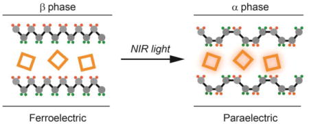
Plasmon-assisted phase transition was used to pattern a freestanding ferroelectric thin film into arrayed domains in a few seconds by incorporating a very small (0.08% by wt.) amount of Au nanocages into the film. The patterned array of ferroelectric domains could serve as discrete pixels for infrared sensing/imaging.
Photothermal conversion based on plasmonic nanostructures has been explored to induce localized heating of the host medium, which is highly attractive for a broad range of applications including biomedicine,[1] steam generation,[2] optofluidics,[3] and acceleration of chemical reactions.[4] The heat transfer from a plasmonic nanoparticle to the host medium starts with the absorption of photons via localized surface plasmon resonance (LSPR) and conversion of part of the photon energy to heat, which is then transferred to the surrounding medium.[5] Previous studies have demonstrated the use of such plasmonic heating to induce phase transition in water,[2b] thermoresponsive copolymers[6] and phase-changing materials[7]. These plasmon-assisted phase transitions in the host media can lead to various interesting physical changes in material properties, offering a powerful tool to design and fabricate functional devices for an array of applications.
Ferroelectric polymers have attracted much interest as the next-generation piezo-/pyroelectric materials due to their feasibility for solution processing, flexibility, low cost, and non-toxicity. Poly(vinylidene fluoride) (PVDF), one of the most commonly used ferroelectric polymers, possesses α, β and γ phases.[8] Its piezo-/pyroelectric properties have enabled the fabrication of film-based tactile sensors, infrared detectors, energy harvesting devices, and non-volatile memories. To realize these applications, it is critical to pattern the ferroelectric phase (either β or γ) rather than the paraelectric α phase. So far, such patterning has been mainly achieved by irradiation etching[9] and imprinting lithography.[10] The former method may deteriorate the ferroelectric properties while it is not easy to obtain a freestanding and smooth polymer film using imprinting lithography without involving multiple steps. PVDF generally exhibits a phase transition from the ferroelectric to the paraelectric phase when heated temperatures near its melting point or the ferroelectric Curie temperature (ca. 170 °C).[11] As an alternative approach, Wegener et al. reported the patterning of PVDF film by scanning of a focused laser beam across the top aluminum electrode.[12] This method successfully generated depolarized stripes of 80–90 μm wide in a PVDF film, but the efficiency is expected to be relatively low due to the high reflectance of the metal electrode, and the one-direction heat transfer from the electrode to the film.
In this communication, we demonstrate the use of plasmonic nanostructures to harvest the photon energy as an effective means to induce ferroelectric-paraelectric phase transition in a ferroelectric polymer film. Specifically, we mixed AuNCs with PVDF and then cast the mixture into thin films. We employed AuNCs as the plasmonic nanostructures owing to their tunable LSPR in the near-infrared (NIR) region and the remarkable photothermal effect.[6, 13] When dispersed in a polymer matrix, AuNCs could be used to generate localized heating in the PVDF film upon laser irradiation, leading to ferroelectric-paraelectric phase transition in just a few seconds. This efficient plasmon-assisted phase transition allows us to pattern the ferroelectric β phase into an array of domains (i.e., pixels) isolated by the paraelectric α phase over a large area, enabling the facile fabrication of NIR-responsive pyroelectric devices.
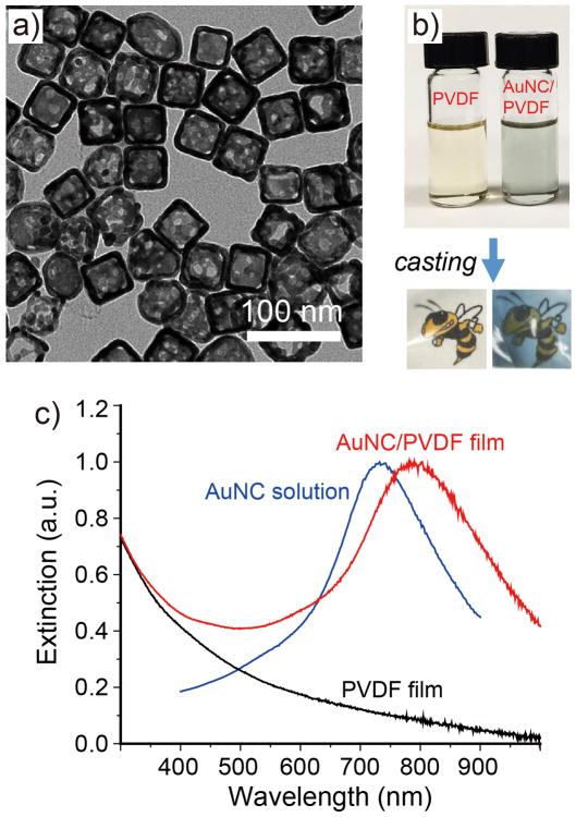
Figure 1a shows a TEM image of the AuNCs, which are characterized by a hollow interior and pores at the corners, together with an average outer edge length of ca. 48 nm and a wall thickness of ca. 6 nm. The homogeneous mixture of AuNCs and PVDF showed a slight blue color (Figure 1b), with no indication of aggregation. The as-obtained AuNC/PVDF composite films had a smooth surface (Figure S1). The films were characterized by FTIR spectroscopy. As shown in Figure S2, the β phase [14] predominated the crystallization of PVDF during film casting and the addition of AuNCs had essentially no effect on the formation of the β phase. The UV-vis-NIR extinction spectrum (Figure 1c) recorded from the AuNC/PVDF film revealed a red shift of ca. 67 nm for the LSPR peak in comparison with that of AuNCs in an aqueous suspension due to the increase in effective refractive index for the surrounding medium.[15] In the present work, we purposely tuned the LSPR peak of the composite film to ca. 800 nm to overlap with the wavelengths of lasers used in this work.
Figure 1.
a) A typical TEM image of AuNCs. b) Photograph of a homogeneous mixture of AuNCs and PVDF obtained by mixing a suspension of AuNCs in ethanol with a PVDF solution in DMF. Transparent films were then cast from the mixture using a mold placed on a hot plate. c) Extinction spectra recorded from an ethanol suspension of AuNCs, PVDF film, and AuNC/PVDF film. The LSPR peak of the AuNCs red-shifted from ca. 733 nm in ethanol to ca. 800 nm in PVDF.
In an initial study, we investigated the plasmon-assisted heating process. The temperatures of a AuNC/PVDF film upon irradiation with the 808 nm laser were monitored using a K-type thermocouple and an infrared camera. We also carried out measurements for pristine PVDF in addition to composite films with four different mass ratios for AuNCs (0.01, 0.02, 0.04 and 0.08%). As shown in Figure S3, the temperature increased with both the mass ratio of AuNCs and laser power density. Within 20 s of irradiation, all the AuNC/PVDF films showed drastic increases in temperature, more significant than what was observed in the case of pristine PVDF film (see Figure S4 for IR images). When the laser power density was increased, the rise in temperature (ΔT) also increased accordingly for each composite film. We then quantitatively evaluated the ability of the composite films to convert light to heat by calculating the energy conversion efficiency (η see Supporting Information). Furthermore, the AuNC/PVDF films exhibited good durability under long-term laser irradiation. As shown in Figure S5, the photothermal conversion efficiency of the composite films did not change after five rounds of irradiation, whereas reduction in temperature rise was clearly observed for a reference sample containing indocyanine green rather than AuNCs. The much higher stability of AuNCs over organic dyes would ensure a long lifetime for the devices.
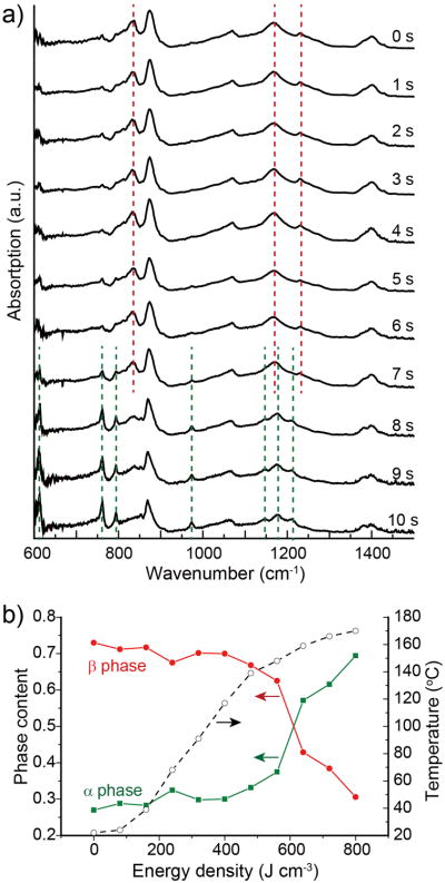
We then studied the phase transition during a plasmon-assisted heating process. We observed that exposure to 808 nm laser at 1 W cm-2 for less than 10 s was sufficient to induce the transition from the ferroelectric β phase to the paraelectric α phase due to the high photothermal conversion efficiency of AuNCs. The formation of the α phase in the composite film was evidenced from the time-elapsed FTIR spectra shown in Figure 2a. The peaks at 610, 765, 796, 973, 1144, 1167 and 1211 cm-1 for the α phase were clearly visible while the peaks at 839, 1176 and 1232 cm-1 for the β phase disappeared. For the thermally induced ferroelectric to paraelectric phase transition of PVDF, it has been reported to occur near its melting point (ca. 170°C) through an intermediate amporphous or liquid-crystalline phase.[11a] When the laser energy added into the AuNC/PVDF film reached 800 J cm-3, the corresponding temperature could be over 170 °C (see Figure 2b). As such, the β-phase crystal could melt to form an amorphous phase or a liquid-crystalline phase, followed by recrystallization into the α phase. We calculated the α or β phase content in the laser-irradiated region from the absorbance of the respective vibrational bands at 765 cm-1 for the α phase and 839 cm-1 for the β phase. Upon irradiation for a short period of only 10 s, the β phase-dominated (ca. 73%) AuNC/PVDF film was transformed to the α phase-dominated (ca. 70%) film.
Figure 2.
a) FTIR spectra recorded from a AuNC/PVDF film upon irradiation with 808 nm laser for different at 1 W cm-2 periods of time. b) Plot of phase content and temperature change in terms of laser power density.
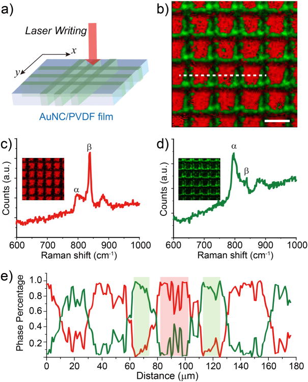
The efficient plasmon-assisted phase transition could also be employed for the fabrication of micropatterned ferroelectric domains. We could simply use a laser beam as a writing pen to create a patterned array of the β-phase PVDF isolated by the nonpolar α phase over a large area. To obtain a micropatterned ferroelectric thin film, a continuous laser beam was utilized to irradiate the AuNC/PVDF film on a motorized x-y stage (Figure 3a). The use of a 785 nm laser at a power of 25 mW and a stage moving speed of 20 μm s-1 successfully produced micropatterned β-phase domains in the composite film. The phase contents of the irradiated and non-irradiated regions were visualized using Raman spectroscopy as shown in Figure 3b. The representative absorption peaks of 839 and 796 cm-1 for the β and α phases, respectively, were selected and the integrated intensity for each peak was mapped (Figure 3, c and d). The pattern clearly shows a transition from the β phase to the α phase in the laser beam path. The percentages of the α and β phases were calculated and plotted as dashed lines in Figure 3e. The line profile clearly shows a patterned distribution of the β phase, with a minimum feature size around 20 μm. Note that there was a transition gap of ca. 10 μm wide between the α and β phase-dominated regions, mainly due to the lateral thermal diffusion.
Figure 3.
a) Schematic illustration of phase patterning in a AuNC/PVDF film using direct laser writing technique. The 785 nm laser source in Raman microscope was used and the motion of the sample was driven by a software-controlled motorized stage installed in the microscope. b) Raman mapping collected over 250 × 250 μm2 area of AuNC/PVDF film, exhibiting a patterned β phase distribution. Bar: 50 μm. Representative Raman spectra of c) non-irradiated region (β phase-dominated) and d) laser-irradiated region (α phase-dominated) in AuNC/PVDF. e) Profile of phase content from the dash line indicated in b).
One of the major applications of the ferroelectric PVDF film is for the detection of infrared signals. Conventionally, the infrared sensor comprises a PVDF film sandwiched between two electrodes with the top electrode severing as an absorption layer to pass the heat to the pyroelectric film.[16] This design may cause heat transfer loss and hinder the pyroelectric response of the detector. In our system, the pyroelectric film itself serves as the adsorption layer due to the incorporation of AuNCs. When the AuNC/PVDF film is exposed to NIR irradiation, heat will be generated directly in the film due to the photothermal effect so the level of polarization in the film will change as a result of change in temperature. Therefore, when the level of polarization decreases upon heating under open circuit conditions, the released surface charges will create a potential difference across the polar axis, similar to a charged parallel plate capacitor.[17] For a parallel capacitor with a homogeneous electric field, the open circuit voltage V can be expressed as
Where p is the pyroelectric coefficient, ε33 is the relative permittivity of the PVDF, d is the film thickness, and ΔT is the temperature change. Therefore, one direct approach to increase the open circuit voltage generated by the AuNC/PVDF film with a specific thickness is to increase the ΔT. At a given irradiation energy, ΔT is determined by the photothermal conversion efficiency (η) of the composite film. As such, we presume that enhancement in pyroelectric response can be obtained for the AuNC/PVDF film by increasing the mass ratio of AuNCs. To measure the pyroelectric responses to NIR irradiation, the PVDF films with different mass ratios of AuNCs were sandwiched between two electrodes, with the bottom electrode being a copper tape and the top electrode being a mesh of Ag nanowires (see Figure S6 for the characterization). As shown in Figure S7, a higher AuNC mass ratio indeed led to a larger temperature change as well as higher voltage value. The 0.08% AuNC/PVDF film developed a voltage of ∼20 mV, which represents an increase of ca. 570% compared to the ∼3 mV for a pristine PVDF reference sample. Clearly, the incorporation of AuNCs could greatly enhance the pyroelectric response of a PVDF-based pyroelectric device to NIR light.
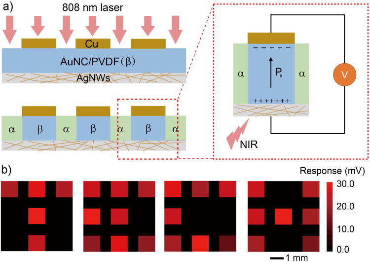
The plasma-assisted micropatterning of ferroelectric phase together with enhanced pyroelectic response further encourage us to fabricate a pixilated array for infrared imaging. As a proof-of-concept, we constructed a β-phase sensing array with 3×3 pixels as shown in Figure S8. The patterned copper layer served as both a mask for laser exposure and electrodes for measuring electrical response (Figure 4a). The array was then selectively exposed to NIR radiation and the open circuit voltage from each pixel was recorded. The electric response of each pixel was then calculated and color-coded to show the difference. Figure 4b showed the illumination patterned to show the four letters of T, E, C, and H. The illuminated pixels generated a signal of 23 ± 5 mV. Negligible signal was detected from the blocked pixels, confirming that the pixels were isolated from each other by the α-phase barrier.
Figure 4.
a) Schematic showing a proof-of-concept device for IR imaging using phase-patterned AuNC/PVDF film by masking the laser irradiation with copper electrodes. b) Responses of pixels in the sensing array to the incident irradiation, which was selectively blocked to form the four letters in TECH.
In conclusion, we have demonstrated the use of plasmonic nanostructures to induce ferroelectric-paraelectric phase transition in a freestanding ferroelectric polymer film. The efficient plasmon-assisted phase transition could be conveniently combined with masked exposure for the fabrication of patterned ferroeleltric domains or pixels. We also demonstrated the feasibility of constructing a pixilated ferroelectric phase pattern for infrared imaging. The simple and efficient method demonstrated in this study is expected to promote both the low-cost fabrication and broader application of polymer-based flexible ferroelectronics.
Supplementary Material
Acknowledgments
This work was supported in part by a grant from the NIH (R01, CA138527) and startup funds from Georgia Tech. As a jointly supervised Ph.D. student from Shandong University, J. L. was also partially supported by a fellowship from the China Scholarship Council.
Contributor Information
Jianhua Li, The Wallace H. Coulter Department of Biomedical Engineering, Georgia Institute of Technology and Emory University, Atlanta, GA 30332 (USA); State Key Laboratory of Crystal Materials, Shandong University, Jinan, Shandong 250100 (P. R. China).
Miaoxin Yang, School of Chemistry and Biochemistry, Georgia Institute of Technology, Atlanta, GA 30332 (USA).
Xiaojun Sun, School of Materials Science and Engineering, Georgia Institute of Technology, Atlanta, GA 30332 (USA).
Dr. Xuan Yang, The Wallace H. Coulter Department of Biomedical Engineering, Georgia Institute of Technology and Emory University, Atlanta, GA 30332 (USA)
Dr. JiaJia Xue, The Wallace H. Coulter Department of Biomedical Engineering, Georgia Institute of Technology and Emory University, Atlanta, GA 30332 (USA)
Dr. Chunlei Zhu, The Wallace H. Coulter Department of Biomedical Engineering, Georgia Institute of Technology and Emory University, Atlanta, GA 30332 (USA)
Prof. Hong Liu, State Key Laboratory of Crystal Materials, Shandong University, Jinan, Shandong 250100 (P. R. China)
Prof. Younan Xia, The Wallace H. Coulter Department of Biomedical Engineering, Georgia Institute of Technology and Emory University, Atlanta, GA 30332 (USA); School of Chemistry and Biochemistry, Georgia Institute of Technology, Atlanta, GA 30332 (USA)
References
- 1.a) Ye E, Win KY, Tan HR, Lin M, Teng CP, Mlayah A, Han MY. J Am Chem Soc. 2011;133:8506–8509. doi: 10.1021/ja202832r. [DOI] [PubMed] [Google Scholar]; b) Huang X, El-Sayed IH, Qian W, El-Sayed MA. J Am Chem Soc. 2006;128:2115–2120. doi: 10.1021/ja057254a. [DOI] [PubMed] [Google Scholar]
- 2.a) Tian L, Luan J, Liu KK, Jiang Q, Tadepalli S, Gupta MK, Naik RR, Singamaneni S. Nano Lett. 2015;16:609–616. doi: 10.1021/acs.nanolett.5b04320. [DOI] [PubMed] [Google Scholar]; b) Zielinski MS, Choi JW, La Grange T, Modestino M, Hashemi SMH, Pu Y, Birkhold S, Hubbell JA, Psaltis D. Nano Lett. 2016;16:2159–2167. doi: 10.1021/acs.nanolett.5b03901. [DOI] [PubMed] [Google Scholar]
- 3.Zeng J, Goldfeld D, Xia Y. Angew Chem Int Ed. 2013;52:4169–4173. doi: 10.1002/anie.201210359. [DOI] [PMC free article] [PubMed] [Google Scholar]; Angew Chem. 2013;125:4263–4267. [Google Scholar]; b) Liu GL, Kim J, Lu Y, Lee LP. Nat Mater. 2006;5:27–32. doi: 10.1038/nmat1528. [DOI] [PubMed] [Google Scholar]
- 4.a) Linic S, Aslam U, Boerigter C, Morabito M. Nat Mater. 2015;14:567–576. doi: 10.1038/nmat4281. [DOI] [PubMed] [Google Scholar]; b) Brongersma ML, Halas NJ, Nordlander P. Nat Nano. 2015;10:25–34. doi: 10.1038/nnano.2014.311. [DOI] [PubMed] [Google Scholar]
- 5.Nguyen SC, Zhang Q, Manthiram K, Ye X, Lomont JP, Harris CB, Weller H, Alivisatos AP. ACS Nano. 2016;10:2144–2151. doi: 10.1021/acsnano.5b06623. [DOI] [PubMed] [Google Scholar]
- 6.Yavuz MS, Cheng Y, Chen J, Cobley CM, Zhang Q, Rycenga M, Xie J, Kim C, Song KH, Schwartz AG. Nat Mater. 2009;8:935–939. doi: 10.1038/nmat2564. [DOI] [PMC free article] [PubMed] [Google Scholar]
- 7.Moon GD, Choi SW, Cai X, Li W, Cho EC, Jeong U, Wang LV, Xia Y. J Am Chem Soc. 2011;133:4762–4765. doi: 10.1021/ja200894u. [DOI] [PMC free article] [PubMed] [Google Scholar]
- 8.Hasegawa R, Takahashi Y, Chatani Y, Tadokoro H. Polym J (Tokyo, Jpn) 1972;3:600–610. [Google Scholar]
- 9.Manohara HM, Morikawa E, Choi J, Sprunger PT. J Microelectromech Syst. 1999;8:417–422. [Google Scholar]
- 10.Kang SJ, Park YJ, Hwang JY, Jeong HJ, Lee JS, Kim KJ, Kim HC, Huh J, Park C. Adv Mater. 2007;19:581–586. [Google Scholar]; b) Liu Y, Weiss DN, Li J. ACS Nano. 2010;4:83–90. doi: 10.1021/nn901397r. [DOI] [PubMed] [Google Scholar]
- 11.Ratri PJ, Tashiro K. Polym J (Tokyo, Jpn) 2013;45:1107–1114. [Google Scholar]; b) Lovinger AJ, Davis DD, Cais RE, Kometani JM. Macromolecules. 1986;19:1491–1494. [Google Scholar]
- 12.Wegener M, Hesse J, Wegener T, Gerhard-Multhaupt R. J Appl Phys. 2002;91:3193–3196. [Google Scholar]
- 13.Skrabalak SE, Chen J, Sun Y, Lu X, Au L, Cobley CM, Xia Y. Acc Chem Res. 2008;41:1587–1595. doi: 10.1021/ar800018v. [DOI] [PMC free article] [PubMed] [Google Scholar]; b) Chen J, Glaus C, Laforest R, Zhang Q, Yang M, Gidding M, Welch MJ, Xia Y. Small. 2010;6:811–817. doi: 10.1002/smll.200902216. [DOI] [PMC free article] [PubMed] [Google Scholar]
- 14.Boccaccio T, Bottino A, Capannelli G, Piaggio P. J Membr Sci. 2002;210:315–329. [Google Scholar]; b) Luo B, Wang X, Wang Y, Li L. J Mater Chem A. 2014;2:510–519. [Google Scholar]
- 15.Mahmoud MA, El-Sayed MA. J Am Chem Soc. 2010;132:12704–12710. doi: 10.1021/ja104532z. [DOI] [PubMed] [Google Scholar]
- 16.Armitage A, Benjamin K, Setiadi D, Weller H, Binnie T. Proc of the Eighth Conference on Sensors and Their Applications, Glasgow; 1997. pp. 297–302. [Google Scholar]; b) Kulkarni ES, Heussler SP, Stier AV, Martin-Fernandez I, Andersen H, Toh CT, Özyilmaz B. Adv Opt Mater. 2015;3:34–38. [Google Scholar]
- 17.Zabek D, Taylor J, Boulbar EL, Bowen CR. Adv Energy Mater. 2015;5 [Google Scholar]
Associated Data
This section collects any data citations, data availability statements, or supplementary materials included in this article.


