Abstract
By first-principles calculations, the magnetism of hole doped tin dichalcogenides SnX2 (X = S, Se) monolayers is systematically studied. It is found that a phase transition from nonmagnetic to ferromagnetic ground state appears once above the critical hole density (~1014 cm−2). The spin magnetic moment can maintain a magnitude of 1.0 μB/hole with excellent stability of ferromagnetic state. Furthermore, we demonstrate that strain is very useful to modulate the DOS near the valence band, resulting in the reduction of the critical hole density to ~1013 cm−2 when the strain reaches 4% (6%) in SnS2 (SnSe2), which can be realized in common field effect transistors. Moreover, the phonon dispersion calculations for the strained SnX2 monolayers indicate that they can keep the dynamical stability under the hole doping. Therefore, the strain tunable magnetic transition in hole doped tin dichalcogenides indicates their potential promising applications in spintronic devices.
Atomically thick two-dimensional (2D) layered materials are currently one of most research interests for their promising applications in electronics, optoelectronics and spintronics1,2,3,4. By introducing local magnetic moments, many 2D systems have been proven to be important candidates in spintronic devices, such as spin field effect transistors (FETs), spin light-emitting diodes (LEDs) and solid-state quantum information processing devices5,6,7,8,9. But 2D semiconductors are naturally nonmagnetic, thereby it is a challenge to generate the stable magnetism. Previous studies have demonstrated that doping 3d transition-metal (TM) ions or 4f rare-earth metal ions into semiconductors were an achievable approach to induce magnetism5,10,11. But the extrinsic ferromagnetism induced by unpaired d or f electrons were undesirable for practical applications, owning to their limiting transports of spin polarized carriers.
In addition to the magnetic elements doping in semiconductors, the type of d0 ferromagnetic semiconductors12,13,14, the absence of atoms with partially filled d or f bands, has received considerable attentions in recent years, due to their intrinsic spontaneous magnetization based on sp states of nonmagnetic atoms. Moreover, these systems indicated obvious advantages in strong long-range exchange coupling interaction and no clustering of magnetic ions. To obtain 2D d0 ferromagnetic semiconductors, most studies have focused on inducing local magnetic moment by introducing nonmagnetic impurity atoms15,16,17, vacancies18,19, as well as manipulating nanoribbon edges20,21,22. In the band-picture model, the spontaneous magnetization in these d0 semiconductors occurs when the relative gain in exchange interaction is larger than the loss in kinetic energy, i.e., when it satisfies the “Stoner Criterion”: D(EF)J > 1, where D(EF) is the density of states (DOS) at the Fermi level (EF), and J denotes the strength of the exchange interaction23. Studies have indicated that J is large enough in elements N, O, P and S valence p orbitals12. When the D(EF) becomes large enough to satisfy the Stoner Criterion, systems can be spin polarized. So the prime purpose of chemical doping and other methods is to increase the DOS at EF. However, these approaches would face serious challenges in experiments, for the structural disorder inherently always causes unnecessary complexity in the physical properties, even the concentration of dopants and vacancies is unfavorable for controlling.
It is worth noting that some 2D semiconductors exist unusual band structures, one of which is the Mexican hat dispersions, such as gallium or indium monochalcogenides, often resulting in van Hove singularities (VHSs) with  divergence in the DOS24,25. Once the EF locates near the top of valence band, the high DOS generally leads an electronic instability, resulting in phase transitions such as magnetism, superconductivity, and other phenomena. In semiconductor industry, carrier doping is considered as an effective approach to modulate EF, which performs obvious advantages including their completely free of structure disorder and remarkably simple to tune physical properties26, compared to previously mentioned approaches. By hole doping in 2D systems, Cao et al.27 reported the theoretical investigation of magnetism in monolayer GaSe, and Huang et al.28 demonstrated a robust half-metallic spin-polarized state in silion phosphides (C2/m Si1P3). In the previous work, we also explored the hole doping effect on magnetic properties in 2D graphene-like C2N29.
In recent years, chemically stable and environmentally friendly semiconducting tin dichalcogenides SnX2 (X = S, Se) have been widely studied for their excellent electrical, optical and magnetic properties, such as lithium ion batteries, photovoltaic devices, as well as field effect transistors30,31,32,33. These studies generally indicated the unusual electronic structure with the high DOS and small dispersion near the top of valence band, which would provide a probability for magnetic phase transition. Although several calculations have demonstrated the magnetism in SnX2 nanostructures, such as manipulating SnSe2 armchair nanoribbons via edge hydrogenation22 and doping metal elements (Li, Mg and Al) in single-layer SnS234, the disadvantage of which would affect their performance in further experiments for their unexpectable complexity and uncontrollability. In this work, by high density hole doping, we mainly study the magnetic characteristic of pristine and strained SnX2 (X = S, Se) monolayers. Results indicate that ferromagnetic ground state with outstanding stability of spin polarization can be obtained by hole doping. Particularly, by strain engineering, the critical hole density can be reduced to 1013 cm−2, which is an order of magnitude smaller than that of pristine structure. Therefore, SnX2 monolayers can be considered as a viable candidates for spintronic devices.
Computational method
To study the electronic and magnetic properties of the SnX2 monolayers, density functional theory (DFT) calculations were performed using the Projector-Augmented Wave (PAW) pseudopotential implementation of the Vienna Ab Initio Simulation Package (VASP)35,36,37. Electron exchange and correlation effects were described by the generalized gradient approximation (GGA) functional of Perdew-Burke-Ernzerhofer (PBE) formula38. The energy cutoff for the plane-wave basis was set as 550 eV on the 11 × 11 × 1 Monkhorst-Pack k-point grid for all simulations. The convergence threshold was 1 × 10⁻⁵ eV for the electronic self-consistent field iterations. The atomic positions were optimized until the maximum Hellma-Feynman force on each atom was less than 10−2 eV Å−1. A vacuum spacing of 20 Å was placed to avoid the interactions between the monolayers and its periodic images. Moreover, to examine the dynamical stability of SnX2 monolayers with doping, the phonon dispersion was calculated by density functional perturbation theory in VASP.
Results and Discussion
SnX2 (X = S, Se) monolayers with the 1T structure are the hexagonal crystal structure of the CdI2-type, as shown in Fig. 1. The SnX2 monolayers consist of three atomic sublayers with the covalently bonded layer of X-Sn-X. The central Sn atom bonds to six nearest-neighbor X atoms located in the top and bottom sublayers. The structural stability of monolayer SnS2 has been theoretically predicted by Zhuang et al.32 For all simulations, the primitive rhombic unit cell was used as the computation unit cell. Before investigating the electronic and magnetic properties, geometric structures of SnX2 were optimized, and atomic positions were relaxed to zero pressure following the convergence criteria. The optimized lattice constant of SnS2 and SnSe2 is 3.700 Å and 3.871 Å, which is in accordance with previous calculations by PBE formula32,33,39.
Figure 1.
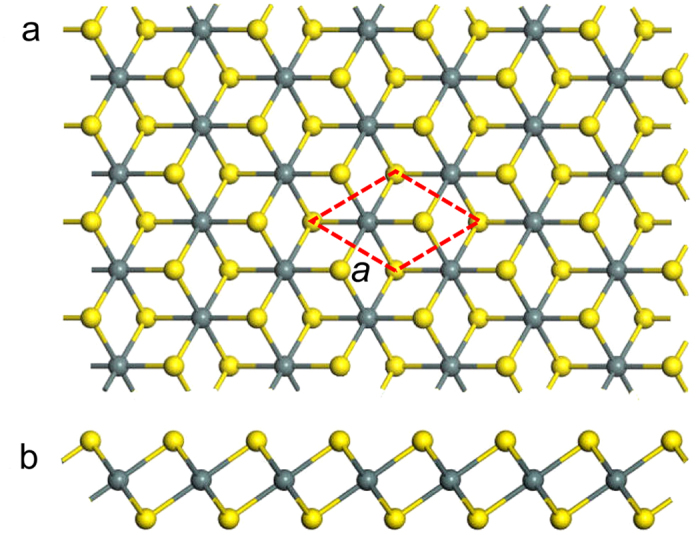
The top view (a) and side view (b) of SnX2 (X = S, Se) monolayers. The yellow and green balls represent X and Sn atoms, respectively. The rhombus with red dashed line represent the primitive unit cell, which is also the computation unit cell.
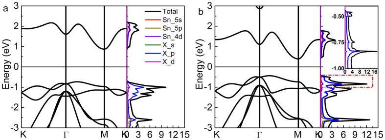
The band structure and DOS of SnX2 monolayers are displayed in Fig. 2. It is obvious that the conduction band minimum (CBM) is located at the M point and the valance band maximum (VBM) lies between Γ − M point, which means both the SnS2 and SnSe2 monolayers are indirect band gap semiconductors. The indirect band gap of SnS2 (~1.60 eV) is almost double of SnSe2 (~ 0.83 eV), which is consistent with previous reported value (1.57 eV for SnS2 and 0.79 eV for SnSe2)39 by the same method. Due to the underestimation by PBE formula, the band gap is smaller than that of previous reports by simulations with Heyd-Scuseria-Ernzerhof (HSE) hybrid functional calculations and quasiparticle self-consistent GW methods32. In order to analyze the contribution of each orbit of atom, the total DOS, together with the 5s, 5p, 4d-orbit partial DOS (PDOS) of Sn atom, and s, p-orbit PDOS of S (Se) atom are depicted in the right diagrams of Fig. 2. It is clear that the high DOS is located around the VBM, which is mainly contributed by S-3p (Se-4p) states, besides, the CBM is co-contributed by Sn-5s and S (Se)-p states.
Figure 2.
Calculated band structure (left) and the total and partial DOS (right) of monolayer SnS2 (a) and SnSe2 (b). The inset map in (b) is the detailed total and partial DOS of SnSe2 near the VBM with the small region of −1.0 to −0.4 eV, as marked in the red dashed rectangle.
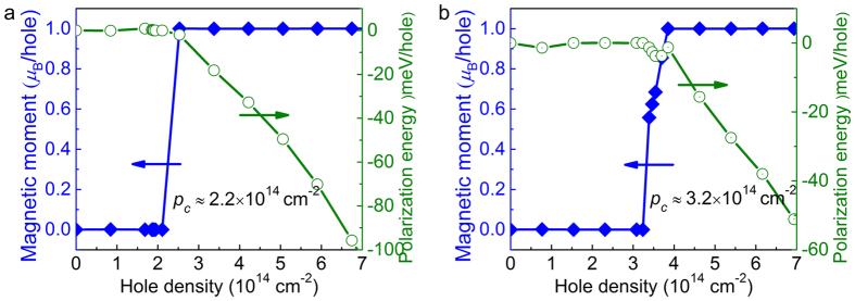
It is well known that the high DOS around the EF would provide the possibility to develop a spontaneous ferromagnetism. We applied carrier doping to investigate the possible ferromagnetism in SnX2 monolayers. Figure 3 shows the local magnetic moment (μB) per hole with the various hole density. At the nonmagnetic state, the magnetic moment is nearly zero. Once above the critical hole density, the local magnetic moment increases rapidly to a constant value with ~1.0 μB/hole, implying the transition from nonmagnetic to ferromagnetic ground state. The critical hole density (pc) of SnS2 and SnSe2 is about 2.2 × 1014 cm−2 and 3.2 × 1014 cm−2, respectively. In order to check the stability of ferromagnetic state, the spin polarization energy per hole, ΔEp, is discussed, which is defined by the energy difference between the spin-polarized state (Esp) and non-spin-polarized state (Enonsp) for each hole, i.e., ΔEp = (Esp − Enonsp)/number(hole). The hole density dependence of spin polarization energy per hole is also shown in Fig. 3. At the spin polarized states, ΔEp decreases monotonically with the increment of the hole density. At the hole density of 7.0 × 1014 cm−2, ΔEp is about −103 and −52 meV/hole for SnS2 and SnSe2, respectively, much higher than those in GaSe (−3 meV/hole)27 and Si1P3 (−24 meV/hole)28, indicating that the ferromagnetic ground state in hole doped SnX2 would be much more stable.
Figure 3.
The magnetic moment and spin polarization energy of monolayer SnS2 (a) and SnSe2 (b), where the blue solid rhombus represent the relation between the magnetic moment and the hole density, and green hollow circle represent the relation between the spin polarization energy and the hole density, respectively.
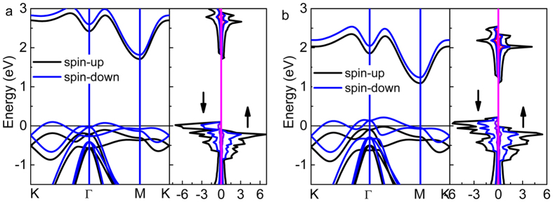
We also studied the band structure and DOS of hole doped SnX2 monolayers. At the first stage, although hole doping leads to the EF shift down to around the VBM, the spin up and spin down bands completely overlap, indicating the nonmagnetic structure. Once the hole density exceeds the critical value, the spin splitting appears around EF, resulting in the magnetic transition. When the hole density continue to increase, the spin up bands shift down, meanwhile, spin down bands shift up gradually. Figure 4 shows the typical electronic structures of hole doped SnX2 in the spin polarized state with the hole density of 4.2 × 1014 cm−2 for SnS2 and 5.4 × 1014 cm−2 for SnSe2. Moreover, it is found that the spin down channel shows metallic characteristic, while the spin up channel shows a fascinate transition from metal to semiconductor, where the transition occurs at 2.5 × 1014 cm−2 for SnS2 and 5.4 × 1014 cm−2 for SnSe2, respectively. Thus, the half-metallic SnX2 monolayers can be modulated by hole doping. This half-metallic property would have good performance in transferring one particular spin oriented electrons such as in a spin filtering devices.
Figure 4.
The typical band structure, and total and partial DOS of monolayer SnX2 in the spin polarized ferromagnetic state, with the hole density of 4.4 × 1014 cm−2 of SnS2 (a) and 5.4 × 1014 cm−2 of SnSe2 (b), respectively. The spin up (↑) and spin down (↓) electronic states are depicted in the right diagram.
To understand the magnetization mechanism of hole doped SnX2 monolayers, we notice that the magnetic moments are contributed mainly by the p states at the VBM. Like the previous study on d0 ferromagnetic semiconductors, such as ZnO12, GaSe27 and SixPy28, the band-picture model also can be employed to explain the magnetization mechanism of hole doped SnX2 monolayers. The ferromagnetic characteristic would be achieved through a p-d hybridization-like p-p interaction between the p states of chalcogens. Figure S1 depicts the evolution of D(EF) and the energy difference ΔE of the two spin-type bands around the VBM by hole doping for monolayer SnX2. A large exchange-splitting of the two spin-type bands appears due to the strong exchange field in the ferromagnetic phase, and the ΔE increases with the increment of hole density when the D(EF) is large enough, which means a large strength of exchange interaction J in these systems. Consequently, the magnetism of SnX2 monolayers can be induced by hole doping.
Currently, ultrahigh carrier density accumulation could be achievable using electric-field control in FETs in experiments, including conventional solid state gated voltage in FETs and electric double layer transistors (EDLTs) by using polymer electrolytes or ionic liquid as gated dielectrics. By using EDLTs, an accumulation of extremely high carrier density could up to 1014 cm−2 in graphene and transitional metal dichalcogenides40,41,42, while ~1013 cm−2 for conventional solid state gated voltage in FETs43,44. But doping with high hole density often brings unexpected uncontrollability and difficulty, even by EDLTs. Therefore, it is crucial to reduce the hole density in SnX2 monolayers for their further practical applications.
The detail DOS of SnSe2 in the small region from −1.0 to −0.4 eV are inset in Fig. 2b. It is find that the high DOS near VBM is located at the deep level, which brings us an insight to analyze the reason why such high critical hole density (~1014 cm−2) must be needed to obtain magnetic transition. Therefore, we devote to modulating the high DOS to the top of valence band. As we known, band structure is highly sensitive to the external conditions such as temperature, pressure or strain, especially in 2D layered structure. They often lead to dramatically changes about electronic, magnetic and optical properties. In particular, the strain engineering is commonly used to tune the band structure, due to the extraordinary break strength and structural stability in a wide range of strain45,46,47,48,49. Zhou et al. recently reported the effects of in-plane biaxial strain on the electronic structure of single-layered SnS250. They found that the tensile strain could result of a larger value of states around the Fermi level. So we believe that the tensile strain should be an effective way to reduce the critical hole density.
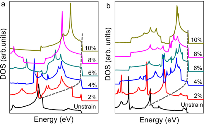
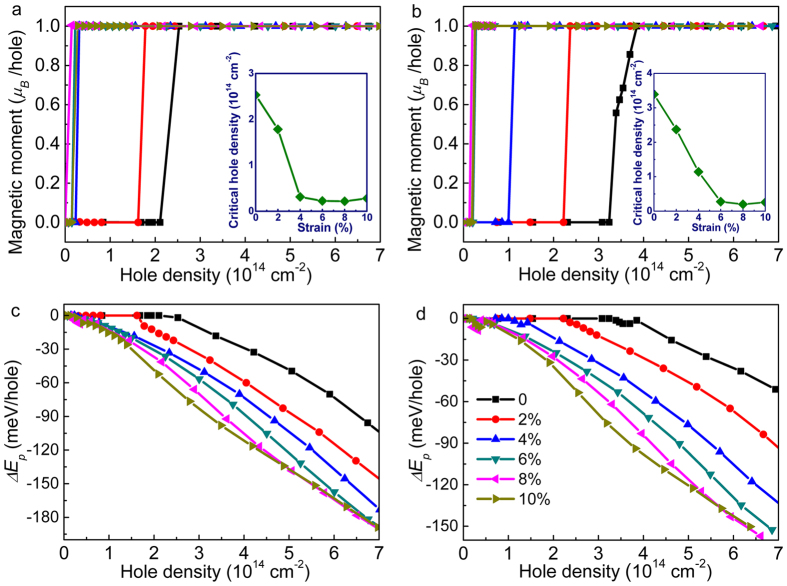
In this study, the biaxial tensile strain [2%, 10%], with the increment of 2%, was applied for the SnX2 monolayers. Figure 5 shows the evolution of DOS near valence band edges for strained SnX2 monolayers, in addition with unstrained states. It is clear that the DOS near the VBM increase with the increment of strain. When the strain reaches 4% for SnS2 and 6% for SnSe2, the DOS around the VBM are similar, and the VHSs occur, due to the Mexican hat-like band edges around Γ point. Once the EF shift down to the top of valence band, such unusual DOS would lead to the reduction of the hole density, and transitions to magnetism. So our next work studies the local magnetic moment and spin polarization energy dependent on the hole density under various strain strength.
Figure 5.
DOS of SnS2 (a) and SnSe2 (b) with biaxial strain from 2% to 10%, in addition with the unstrained state. The gray dashed lines indicate the location of the high DOS near VBM.
The relations between the spin magnetic moment/hole and the hole density are shown in Fig. 6a and b. At the initial strained SnX2 monolayers without hole doping, it is nonmagnetic at the ground state. The magnetic moment (~1.0 μB/hole) appears at the lower hole density in comparison to the unstrained SnX2. The inset map plotted relations between the critical hole density and the tensile strain. The critical hole densities reduce sharply in the small range of strain, i.e., 0–4% for SnS2 and 0–6% for SnSe2, and then maintain about 1.5 × 1013 cm−2 of SnS2 and 2.0 × 1013 cm−2 of SnSe2, respectively. These values are an order lower than that of unstrained structures, and could be realized in common FETs. Moreover, with the biaxial strain applied, the tendency of critical hole density is consist with that of DOS around the VBM described in Fig. 5. In addition, Fig. S1 also shows the D(EF) and ΔE for strained SnS2 (SnSe2) monolayers. It is clear that the SnX2 monolayers under biaxial strain are more favorable to achieve the spin splitting due to the greatly enhanced D(EF). Next, we check the stability of spin polarization of the strained structure, as shown in Fig. 6c and d. It is obvious that the spin polarization energy/hole reduce monotonously at the magnetic state in a large range of hole density. Compared to the unstrained SnX2 monolayers, the lower spin polarization energy/hole can be obtained with the increment of strain, and finally the spin polarization energy nearly tend to the constant value. For example, at the hole density of 7.0 × 1014 cm−2 with 6% strain applied, values decrease monotonically to −180 meV of SnS2 and −160 meV of SnSe2, which is far more small than that of the unstrained structure. Therefore, by applying tensile strain, the magnetism of SnX2 monolayers would have promising applications for their achievable hole doping density and stable magnetic phase transition.
Figure 6.
The magnetic moment/hole of SnS2 (a) and SnSe2 (b) with biaxial strain applied [2%, 10%] in the large range of 0~7.0 × 1014 cm−2, where the inset represent relations between the critical hole density and tensile strain. (c) and (d) Depict the spin polarization energy/hole of SnS2 and SnSe2, respectively. The magnetic moment/hole and spin polarization energy/hole of unstrained structure are also marked in (a–d) with black color.
In addition, the critical hole density, magnetic moment and spin polarization energy are summarized for SnX2 in Table 1, in comparison with GaSe27 and C2/m Si1P328. The magnetism in unstrained structure requires higher hole density doping. But applying tensile strain (≥4% for SnS2 and ≥6% for SnSe2), the critical hole density of SnX2 monolayers is smaller that of Si1P3 and GaSe. Furthermore, SnX2 monolayers perform better stability of spin polarization under both unstrained and strained state. Therefore, for 2D SnX2 monolayers, hole doping can induce stable spin polarization in a large range of hole density, and the critical hole density and spin polarization energy can be improved greatly by strain engineering.
Table 1. The critical hole density, magnetic moment and spin polarization energy for SnX2, GaSe, and C2/m Si1P3 are summarized, where ΔE p of SnX2 gives the value at the hole density of 7.0 × 1014 cm−2.
| SnS2 | SnSe2 | SnS2 (4%) | SnSe2 (6%) | GaSe | Si1P3 | |
|---|---|---|---|---|---|---|
| Critical hole density (1013 cm−2) | 22.4 | 32.3 | 1.5 | 2.0 | 3.0 | 9.0 |
| Magnetic moment (μB/hole) | 1.0 | 1.0 | 1.0 | 1.0 | 0.9 | 0.98 |
| ΔEp (meV/hole) | −103 | −52 | −170 | −160 | −3 | −23 |
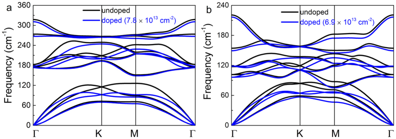
The stability of hole doped SnX2 monolayers is crucial for their applications on magnetism. So, we have also carried out the phonon dispersion calculations to study their dynamic stabilities. The phonon dispersions of SnS2 (SnSe2) monolayers under the tensile strain of 4% (6%) are shown in Fig. 7. No imaginary frequency is found under the tensile strain, indicating the SnS2 (SnSe2) monolayers under tensile strain are stable. At 0.1 hole per unit cell doping, large enough to induce magnetism in SnS2 (SnSe2) monolayer with tensile strain of 4% (6%), there is still no imaginary frequency, except the frequency softening comparing to the SnS2 (SnSe2) monolayers without doping. Therefore, these results indicate that hole doping in SnX2 monolayers have negligible effect on their structural stabilities, and will provide feasible theoretical predictions for practical applications in spintronic devices.
Figure 7. The phonon dispersion with 4% (6%) strain for SnS2 (SnSe2), where blue lines represent the hole density of 0.1 hole per unit cell, i.e., 7.8 × 1013 cm−2 for SnS2 and 6.9 × 1013 cm−2 for SnSe2.
The results of undoped strained states are depicted in (a) and (b) with black color as well for comparison.
Conclusions
In conclusion, electronic and magnetic properties of the SnX2 (X = S, Se) monolayers are studied by DFT calculations. It is demonstrated that hole doping (~1014 cm−2) can drive a phase transition from nonmagnetic to ferromagnetic ground state. The electron spin magnetic moment can reach a constant magnitude (~1.0 μB/hole) with excellent stability of ferromagnetic state. Besides, the half-metallic characteristic can be modulated by hole doping. Furthermore, by introducing tensile biaxial strain to SnX2 monolayers, the critical hole density can reduce to ~1013 cm−2, which could be realized by conventional solid high dielectric FETs. The higher spin polarization energy indicates better stability in comparison with the pristine structure. In addition, the hole doped SnX2 monolayers still remains stable by phonon dispersion calculations. Therefore, investigation of the magnetism for hole doped SnX2 monolayers under the strain will provide an achievable idea for 2D functional materials in spintronics.
Additional Information
How to cite this article: Xiang, H. et al. Strain tunable magnetism in SnX2 (X = S, Se) monolayers by hole doping. Sci. Rep. 6, 39218; doi: 10.1038/srep39218 (2016).
Publisher's note: Springer Nature remains neutral with regard to jurisdictional claims in published maps and institutional affiliations.
Supplementary Material
Acknowledgments
This work was supported by the Fundamental Research Funds for the Central Universities, a Project Funded by the Priority Academic Program Development of Jiangsu Higher Education Institutions (PAPD). We are grateful for the support of NSFC (51672126). The calculations were performed on parallel computers at the High Performance Computing Center (HPCC) of Nanjing University.
Footnotes
Author Contributions H.X., B.X. and J.Y. designed and conduct the calculations. B.X., Y.X. and Z.L. analyzed the data. H.X. and B.X. wrote the main manuscript. J.Y. and Z.L. revised the manuscript. All authors reviewed and approved the final revision of this manuscript.
References
- Watanabe K., Taniguchi T. & Kanda H. Direct-bandgap properties and evidence for ultraviolet lasing of hexagonal boron nitride single crystal. Nat. Mater. 3, 404–409 (2004). [DOI] [PubMed] [Google Scholar]
- Novoselov K. S. et al. Electric field effect in atomically thin carbon films. Science 206, 666–669 (2004). [DOI] [PubMed] [Google Scholar]
- Radisavljevic B., Radenovic A., Brivio J., Giacometti V. & Kis A. Single-layer MoS2 transistors. Nature Nanotech. 6, 147–150 (2011). [DOI] [PubMed] [Google Scholar]
- Xu B. et al. Two-dimensional graphene-like C2N: An experimentally available porous membrane for hydrogen purification. Phys. Chem. Chem. Phys. 17, 15115–15118 (2015). [DOI] [PubMed] [Google Scholar]
- Sevinçli H., Topsakal M., Durgun E. & Ciraci S. Electronic and magnetic properties of 3d transition-metal atom adsorbed graphene and graphene nanoribbons. Phys. Rev. B 77, 195434 (2008). [Google Scholar]
- Ma Y. et al. Evidence of the existence of magnetism in pristine VX2 monolayers (X = S, Se) and their strain-induced tunable magnetic properties. ACS nano 6, 1695–1701 (2012). [DOI] [PubMed] [Google Scholar]
- Dolui K., Rungger I., Das Pemmaraju C. & Sanvito S. Possible doping strategies for MoS2 monolayers: An ab initio study. Phys. Rev. B 88, 075420 (2013). [Google Scholar]
- Chang T. R., Lin H., Jeng H. T. & Bansil A. Thickness dependence of spin polarization and electronic structure of ultra-thin films of MoS2 and related transition-metal dichalcogenides. Sci. Rep. 4, 6270 (2014). [DOI] [PMC free article] [PubMed] [Google Scholar]
- Yang S. et al. Tuning the optical, magnetic, and electrical properties of ReSe2 by nanoscale strain engineering. Nano lett. 15, 1660–1666 (2015). [DOI] [PubMed] [Google Scholar]
- Cheng Y. C., Zhu Z. Y., Mi W. B., Guo Z. B. & Schwingenschlögl U. Prediction of two-dimensional diluted magnetic semiconductors: Doped monolayer MoS2 systems. Phys. Rev. B 87, 100401 (2013). [Google Scholar]
- Ramasubramaniam A. & Naveh D. Mn-doped monolayer MoS2: An atomically thin dilute magnetic semiconductor. Phys. Rev. B 87, 195201 (2013). [Google Scholar]
- Peng H. et al. Origin and enhancement of hole-induced ferromagnetism in first-row d0 semiconductors. Phys. Rev. Lett. 102, 017201 (2009). [DOI] [PubMed] [Google Scholar]
- Venkatesan M., Fitzgerald C. B. & Coey J. M. D. Thin films unexpected magnetism in a dielectric oxide. Nature 430, 630 (2004). [DOI] [PubMed] [Google Scholar]
- Coey J. M. D. d0 ferromagnetism. Solid State Sci. 7, 660–667 (2005). [Google Scholar]
- Yue Q., Chang S., Qin S. & Li J. Functionalization of monolayer MoS2 by substitutional doping: A first-principles study. Phys. Lett. A 377, 1362–1367 (2013). [Google Scholar]
- Cakir D., Sahin H. & Peeters F. M. Doping of rhenium disulfide monolayers: A systematic first principles study. Phys. Chem. Chem. Phys. 16, 16771–16779 (2014). [DOI] [PubMed] [Google Scholar]
- Hu A.-M., Wang L.-l., Xiao W.-Z., Xiao G. & Rong Q.-Y. Electronic structures and magnetic properties in nonmetallic element substituted MoS2 monolayer. Comput. Mater. Sci. 107, 72–78 (2015). [Google Scholar]
- Yazyev O. V. & Helm L. Defect-induced magnetism in graphene. Phys. Rev. B 75, 125408 (2007). [Google Scholar]
- Palacios J. J., Fernández-Rossier J. & Brey L. Vacancy-induced magnetism in graphene and graphene ribbons. Phys. Rev. B 77, 195428 (2008). [Google Scholar]
- Li H. et al. Electronic structure and magnetic properties of GaN sheets and nanoribbons. J. Phys. Chem. C 114, 11390–11394 (2010). [Google Scholar]
- Lu P., Wu X., Guo W. & Zeng X. C. Strain-dependent electronic and magnetic properties of MoS2 monolayer, bilayer, nanoribbons and nanotubes. Phys. Chem. Chem. Phys. 14, 13035–13040 (2012). [DOI] [PubMed] [Google Scholar]
- Huang Y., Ling C., Liu H. & Wang S. Tuning electronic and magnetic properties of SnSe2 armchair nanoribbons via edge hydrogenation. J. Mater. Chem. C 2, 10175–10183 (2014). [Google Scholar]
- Mielke A. & Tasaki H. Ferromagnetism in the Hubbard model. Commun. Math. Phys. 158, 341–371 (1993). [Google Scholar]
- Zólyomi V., Drummond N. D. & Fal’ko V. I. Band structure and optical transitions in atomic layers of hexagonal gallium chalcogenides. Phys. Rev. B 87, 195403 (2013). [Google Scholar]
- Wickramaratne D., Zahid F. & Lake R. K. Electronic and thermoelectric properties of van der Waals materials with ring-shaped valence bands. J. Appl. Phys. 118, 075101 (2015). [Google Scholar]
- Yuan H. et al. High-density carrier accumulation in ZnO field-effect transistors gated by electric double layers of ionic liquids. Adv. Funct. Mater. 19, 1046–1053 (2009). [Google Scholar]
- Cao T., Li Z. & Louie S. G. Tunable magnetism and half-metallicity in hole-doped monolayer GaSe. Phys. Rev. Lett. 114, 236602 (2015). [DOI] [PubMed] [Google Scholar]
- Huang B., Zhuang H. L., Yoon M., Sumpter B. G. & Wei S.-H. Highly stable two-dimensional silicon phosphides: Different stoichiometries and exotic electronic properties. Phys. Rev. B 91, 121401 (2015). [Google Scholar]
- Liang Z. et al. Carrier-tunable magnetism in two dimensional graphene-like C2N. RSC Adv. 6, 54027–54031 (2016). [Google Scholar]
- Seo J.-w. et al. Two-dimensional SnS2 nanoplates with extraordinary high discharge capacity for lithium ion batteries. Adv. Mater. 20, 4269–4273 (2008). [Google Scholar]
- Wahnon P. et al. V-doped SnS2: a new intermediate band material for a better use of the solar spectrum. Phys. Chem. Chem. Phys. 13, 20401–20407 (2011). [DOI] [PubMed] [Google Scholar]
- Zhuang H. L. & Hennig R. G. Theoretical perspective of photocatalytic properties of single-layer SnS2. Phys. Rev. B 88, 115314 (2013). [Google Scholar]
- Xia C. et al. The characteristics of n- and p-type dopants in SnS2 monolayer nanosheets. Phys. Chem. Chem. Phys. 16, 19674–19680 (2014). [DOI] [PubMed] [Google Scholar]
- Yu D., Liu Y., Sun L., Wu P. & Zhou W. Density functional study on the hole doping of single-layer SnS2 with metal element X (X = Li, Mg, and Al). Phys. Chem. Chem. Phys. 18, 318–324 (2016). [DOI] [PubMed] [Google Scholar]
- Kresse G. & Hafner J. Ab initiomolecular dynamics for liquid metals. Phys. Rev. B 47, 558–561 (1993). [DOI] [PubMed] [Google Scholar]
- Kresse G. & Furthmüller J. Efficiency of ab-initio total energy calculations for metals and semiconductors using a plane-wave basis set. Comput. Mater. Sci. 6, 15–50 (1996). [DOI] [PubMed] [Google Scholar]
- Kresse G. & Furthmüller J. Efficient iterative schemes for ab initio total-energy calculations using a plane-wave basis set. Phys. Rev. B 54, 11169–11186 (1996). [DOI] [PubMed] [Google Scholar]
- Perdew J. P., Burke K. & Ernzerhof M. Generalized gradient approximation made simple. Phys. Rev. Lett. 77, 3865–3868 (1996). [DOI] [PubMed] [Google Scholar]
- Huang Y., Ling C., Liu H., Wang S. & Geng B. Versatile electronic and magnetic properties of SnSe2 nanostructures induced by the strain. J. Phys. Chem. C 118, 9251–9260 (2014). [Google Scholar]
- Efetov D. K. & Kim P. Controlling electron-phonon interactions in graphene at ultrahigh carrier densities. Phys. Rev. Lett. 105, 256805 (2010). [DOI] [PubMed] [Google Scholar]
- Braga D., Gutierrez Lezama I., Berger H. & Morpurgo A. F. Quantitative determination of the band gap of WS2 with ambipolar ionic liquid-gated transistors. Nano lett. 12, 5218–5223 (2012). [DOI] [PubMed] [Google Scholar]
- Zhang Y., Ye J., Matsuhashi Y. & Iwasa Y. Ambipolar MoS2 thin flake transistors. Nano lett. 12, 1136–1140 (2012). [DOI] [PubMed] [Google Scholar]
- Mak K. F. et al. Tightly bound trions in monolayer MoS2. Nat. Mater. 12, 207–211 (2013). [DOI] [PubMed] [Google Scholar]
- Zhang Y. J., Oka T., Suzuki R., Ye J. T. & Iwasa Y. Electrically switchable chiral light-emitting transistor. Science 344, 725–728 (2014). [DOI] [PubMed] [Google Scholar]
- Lee C., Wei X., Kysar J. W. & Hone J. Measurement of the elastic properties and intrinsic strength of monolayer graphene. Science 321, 385–388 (2008). [DOI] [PubMed] [Google Scholar]
- Li T. Ideal strength and phonon instability in single-layer MoS2. Phys. Rev. B 85, 235407 (2012). [Google Scholar]
- Conley H. J. et al. Bandgap engineering of strained monolayer and bilayer MoS2. Nano lett. 13, 3626–3630 (2013). [DOI] [PubMed] [Google Scholar]
- Fei R. & Yang L. Strain-engineering the anisotropic electrical conductance of few-layer black phosphorus. Nano lett. 14, 2884–2889 (2014). [DOI] [PubMed] [Google Scholar]
- Liu X., Wang Y., Li F. & Li Y. Two-dimensional stanane: strain-tunable electronic structure, high carrier mobility, and pronounced light absorption. Phys. Chem. Chem. Phys. 18, 14638–14643 (2016). [DOI] [PubMed] [Google Scholar]
- Zhou W. & Umezawa N. Insight into the band structure engineering of single-layer SnS2 with in-plane biaxial strain. Phys. Chem. Chem. Phys. 18, 7860–7865 (2016). [DOI] [PubMed] [Google Scholar]
Associated Data
This section collects any data citations, data availability statements, or supplementary materials included in this article.


