Significance
Nanoelectronic transistor sensors based on synthesized one- and two-dimensional nanomaterials have achieved real-time label-free detection of a wide range of biological species with high sensitivity, although direct analysis of biological samples has been limited due to Debye charge screening in physiological solutions. This paper describes a general strategy overcoming this challenge involving comodification of the transistor sensor surface with a polymer and receptor, where the polymer forms a permeable layer that increases the effective screening length and receptor enables selective detection of analytes. The capability of this strategy was demonstrated with selective detection of cancer markers in physiological solution, thus opening substantial opportunities for real-time sensing applications in biology and medicine.
Keywords: field-effect transistor, Debye screening, surface modification, DNA aptamer receptor, polyethylene glycol
Abstract
Nanomaterial-based field-effect transistor (FET) sensors are capable of label-free real-time chemical and biological detection with high sensitivity and spatial resolution, although direct measurements in high–ionic-strength physiological solutions remain challenging due to the Debye screening effect. Recently, we demonstrated a general strategy to overcome this challenge by incorporating a biomolecule-permeable polymer layer on the surface of silicon nanowire FET sensors. The permeable polymer layer can increase the effective screening length immediately adjacent to the device surface and thereby enable real-time detection of biomolecules in high–ionic-strength solutions. Here, we describe studies demonstrating both the generality of this concept and application to specific protein detection using graphene FET sensors. Concentration-dependent measurements made with polyethylene glycol (PEG)-modified graphene devices exhibited real-time reversible detection of prostate specific antigen (PSA) from 1 to 1,000 nM in 100 mM phosphate buffer. In addition, comodification of graphene devices with PEG and DNA aptamers yielded specific irreversible binding and detection of PSA in pH 7.4 1x PBS solutions, whereas control experiments with proteins that do not bind to the aptamer showed smaller reversible signals. In addition, the active aptamer receptor of the modified graphene devices could be regenerated to yield multiuse selective PSA sensing under physiological conditions. The current work presents an important concept toward the application of nanomaterial-based FET sensors for biochemical sensing in physiological environments and thus could lead to powerful tools for basic research and healthcare.
Nanoelectronic biosensors offer broad capabilities for label-free high-sensitivity real-time detection of biological species that are important to both fundamental research and biomedical applications (1–6). In particular, field-effect transistor (FET) biosensors configured from semiconducting nanowires (1, 2), single-walled carbon nanotubes (1, 3, 4), and graphene (1, 5, 6) have been extensively investigated since the first report of real-time protein detection using silicon nanowire devices (7). Subsequent studies have demonstrated highly sensitive and in some cases multiplexed detection of key analytes, including protein disease markers (8–10), nucleic acids (11–13), and viruses (14), as well as detection of protein–protein interactions (8, 15–17) and enzymatic activity (8).
The success achieved with nanomaterial-based FET biosensors has been limited primarily to measurements in relatively low–ionic-strength nonphysiological solutions due to the Debye screening length (18, 19). In short, the screening length in physiological solutions, <1 nm, reduces the field produced by charged macromolecules at the FET surface and thus makes real-time label-free detection difficult. The first method reported to overcome this intrinsic limitation of FET biosensors involved desalting to enable subsequent low–ionic-strength detection (8, 20), although this also precludes true real-time measurements. Truncated antibody receptors (21) and small aptamers (22) also have been used to reduce the distance between target species and the FET surfaces, although the generality of such methods for real-time sensing in physiological conditions requires further study. In addition, recent work has shown that high-frequency mixing-based detection can be used to overcome Debye screening effects (23, 24), although the device geometry may limit this approach in cellular and in vivo applications.
Recently, we have developed a strategy to overcome the Debye screening limitation that involves modification of a FET sensor surface with a biomolecule-permeable polymer layer to increase the effective screening length in the region immediately adjacent to the device, and demonstrated this concept for nonspecific detection of PSA using silicon nanowire sensors in physiological solutions (25). To explore the generality of this approach for nanomaterials-based FET sensors and further extend the concept to selective analyte recognition and detection, we herein describe studies demonstrating controlled nonspecific and highly selective protein detection in physiological media using graphene FET sensors in which the device surfaces are modified only with a biomolecule-permeable polymer layer and comodified with DNA aptamer/biomolecule-permeable polymer layer, respectively.
Results and Discussion
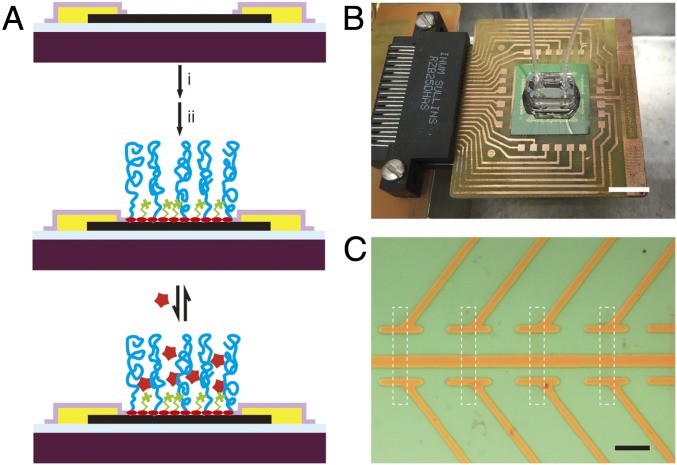
To realize the biodetection in physiological solutions, a biomolecule-permeable polymer layer was constructed by surface modification as illustrated in Fig. 1A (Materials and Methods). This modification strategy involves (i) adsorption of pyrene butyric acid (PYCOOH) via π–π stacking to introduce functional carboxyl groups on the graphene surface (26, 27), followed by (ii) covalent cocoupling of amine-terminated 10-kDa polyethylene glycol (PEG) and either the spacer molecule ethanolamine (ETA) or a DNA aptamer as a specific protein receptor. The coupling procedure (Materials and Methods) (28) uses 1-ethyl-3-[3-dimethylaminopropyl]carbodiimide hydrochloride (EDC) and N-hydroxysulfosuccinimide (Sulfo-NHS) to couple PEG/ETA and PEG/aptamer to the carboxyl groups of PYCOOH-modified graphene device surfaces.
Fig. 1.
Active sensor surface and sensor chip. (A) Illustration of a graphene FET device with comodification of PEG and a small-molecule spacer or PEG and a receptor, for nonspecific and specific detection of the analyte, respectively. Dark purple, silicon wafer; light blue, 600-nm SiO2; black, graphene; yellow, metal contact; light purple, Si3N4 passivation layer; red oval, PYCOOH; green, spacer molecule; blue, PEG chain; red star, analyte. EDC and Sulfo-NHS serve as cross-linkers to couple PYCOOH with PEG and spacer molecules. (B) Optical image of a typical device chip (central green square) mounted on a PCB interface board that is plugged into the input/output interface connected to a computer-controlled data acquisition system. The copper squares surrounding the device chip are connected to the chip by wire bonding. A PDMS microfluidic channel is mounted onto the central graphene region. The inlet/outlet of solution was controlled with a syringe pump via tubing. (Scale bar: 1 cm.) (C) Bright-field microscopy image of two types of graphene channels with dimensions of 5 × 5 and 5 × 10 μm, sharing the common source (S) with individually addressable drain (D) contacts. The white dashed rectangle highlights one graphene FET. (Scale bar: 20 μm.)
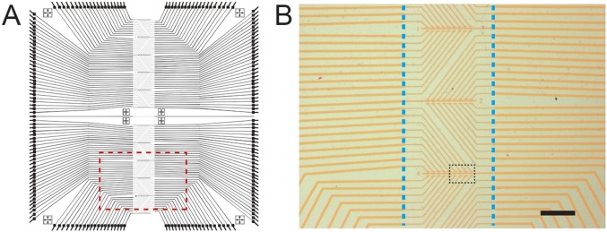
Our sensor chip (Fig. 1B) consists of a FET array with nominally 180 individually addressable graphene devices (see Fig. S1 for full device layout) and was fabricated as follows. First, graphene was synthesized using chemical vapor deposition (CVD) and transferred onto the SiO2 surface of a Si device fabrication wafer (29). Second, the graphene FET channels were defined by photolithography, and then passivated metal source/drain contacts were fabricated by a second photolithography step, metal thermal evaporation, and sputtered Si3N4 (Materials and Methods). Completed device chips were attached and wire-bonded to standard printed circuit boards (PCBs) for interfacing to measurement electronics, and a poly(dimethylsiloxane) (PDMS) microfluidic channel was mounted over the central device region for delivery of analyte solutions using a syringe pump (Fig. 1B; Materials and Methods). An optical image (Fig. 1C) shows two types of graphene channels with dimensions of 5 × 5 and 5 × 10 μm sharing the common source (S) with individually addressable drain (D) contacts.
Fig. S1.
Sensor chip device layout. (A) Overall layout of the sensor chip consisting of 180 individually addressable graphene transistors. The thicker outer lines correspond to gold metal interconnects, which terminate at wire-bonding pads at the chip periphery, and the thinner lines in the central vertical region correspond to the source and drain connections. Image size: 10 × 10 mm2. (B) Optical image of graphene devices from the region highlighted by red-dashed box in A. The yellow–orange lines correspond to the gold metal source and drain electrodes that connect individual graphene devices. The position of the microfluidic channel used to deliver samples is highlighted by the two vertical dashed blue lines. (Scale bar: 100 μm.) The black dashed box highlights the region corresponding to Fig. 1C.
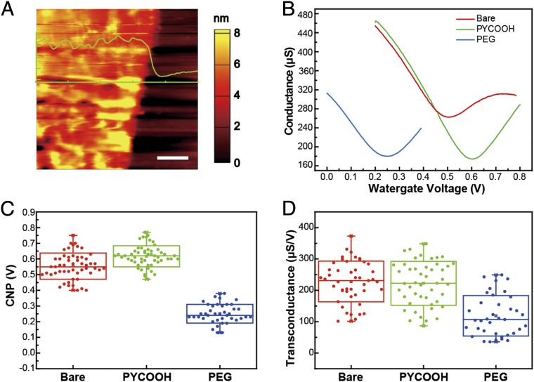
The properties of functionalized graphene and graphene devices were characterized by several complementary methods before carrying out sensing measurements. First, atomic force microscopy (AFM) studies of PEG-modified graphene devices carried out in 1× PBS (Fig. 2A; Materials and Methods) show a well-defined 6- to 8-nm step between the PEG-modified graphene FET channel and the SiO2/Si substrate. Similar AFM measurements on unmodified graphene devices, which show a 0.7- to 1-nm step, and Raman mapping (SI Text and Fig. S2) are consistent with monolayer graphene (30, 31). These data indicate that the thickness of the PEG layer on the graphene devices is ∼5–7 nm, which is consistent with previous indentation measurements of PEG layers carried out by AFM (32). In addition, the AFM measurements show that the PEG layer was only observed on graphene, indicating that the PYCOOH initial modification was specific only to the graphene devices as expected (27), and thus allows for selective functionalization of the graphene sensor surfaces.
Fig. 2.
Characterizations of modified graphene surfaces. (A) AFM image shows an ∼6- to 8-nm PEG layer in 1× PBS on the graphene FET channel with respect to the SiO2/Si substrate. (Scale bar: 1 μm.) (B) Conductance vs. water-gate voltage data recorded from a typical device (source/drain voltage, 100 mV) in 1× PBS before and after sequential modification steps: bare graphene (red), and PYCOOH- (green) and PEG-modified graphene (blue). (C) Box plots of CNPs on 46 bare graphene (red), 46 PYCOOH-modified (green), and 37 PEG-modified graphene devices (blue). (D) Box plots of the transconductance before and after PYCOOH (green) and PEG (blue) modifications. The highest and lowest horizontal lines in the boxes in C and D represent the SD, whereas the middle line represents the mean value. The vertical whiskers show the maximum and minimum values.
Fig. S2.
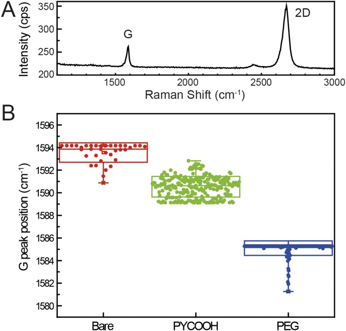
Raman characterization of graphene before and after surface modification steps. (A) Raman spectrum of bare graphene, where the graphene was transferred to a SiO2/Si substrate. The G and 2D bands (SI Text) are highlighted. (B) Box plots of Raman G peak shift before and after PYCOOH and PEG modifications measured from a 10 × 10-μm2 graphene region. The highest and lowest horizontal lines in the boxes represent SD, whereas the middle line represents the mean value. The vertical lines highlight the maximum and minimum values. The average G peaks of pristine graphene (red), PYCOOH-modified graphene (green), and PEG-modified graphene (blue) are located at 1,594, 1,591, and 1,585 cm−1, respectively. The downshift of the G band indicates electron doping due to the PYCOOH and then PEG modification steps. Raman spectra were acquired with a LabRam Evolution Multiline Raman Spectrometer (Horiba) equipped with 600 blaze/mm grating and a 100× microscope objective lens (numerical aperture of 0.95) and 532-nm wavelength continuous-wave diode laser.
Second, device electrical measurements (Fig. 2 B–D) highlight several additional points relevant to graphene FET sensors. Conductance versus water-gate voltage data obtained from the same graphene device during sequential modification steps (Fig. 2B; Materials and Methods) show that the charge neutrality point (CNP) of bare graphene device, 0.51 V, increases to 0.60 V and then decreases to 0.25 V after PYCOOH and PEG modification, respectively. CNP measurements recorded from 46 devices during the sequential modification steps (Fig. 2C) yielded average ±1 SD values of 0.55 ± 0.08, 0.62 ± 0.07, and 0.22 ± 0.06 for bare, PYCOOH-modified, and PEG-modified devices, respectively. These values suggest that the bare graphene was initially p-doped and that PEG-modification leads to n-doping of the devices (33). This overall doping effect was confirmed by Raman spectroscopy mapping (SI Text and Fig. S2), which showed a 1,594–1,585 cm−1 G band shift in bare to PEG-modified graphene. Last, the PEG layer on graphene devices yielded a statistically significant drop (P < 0.001, double-sided t test) of the transconductance, from 228 ± 65 µS/V before modification to 119 ± 64 µS/V after completion of the PEG modification (Fig. 2D). These results are consistent with previous observations for PEG-modified silicon nanowire FETs (25), and moreover, an estimate of the effective dielectric constant of the PEG layer (SI Text) supports the hypothesis that this permeable layer reduces the effective dielectric constant at sensor surface compared with aqueous solution.
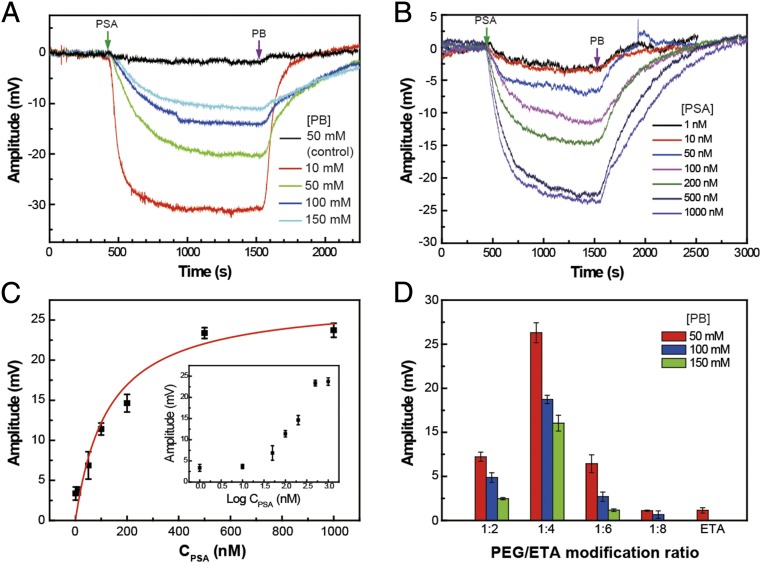
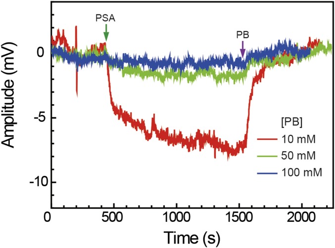
Initial PSA-sensing measurements carried out with ETA and a 1:4 PEG:ETA-modified graphene devices in pH 6 phosphate buffer (PB) as a function of solution ionic strength (Fig. 3A) exhibited substantial differences for detection of fixed concentration PSA (pI = 6.8–7.5) (34, 35). First, measurements made on ETA-modified graphene devices exhibit an easily detected signal at 10 mM PB that rapidly drops to near baseline at 50 mM (black trace, Fig. 3A and Fig. S3). No detectable PSA response was observed in 100 mM PB, which has a ∼0.7-nm Debye length (25) comparable with physiological solution. In contrast, PEG/ETA-modified devices show only a gradual decrease in PSA-sensing signal with increasing PB concentration. The signal response in 100 mM PB, ∼14 mV, exceeds the signal recorded from ETA-modified devices in 10 mM PB, and moreover, well-defined sensing signals, ∼11 mV, can still be recorded in 150 mM PB where the Debye length is ∼0.5 nm (25). In addition, these data show that PSA sensing is reversible with the device conductance returning to baseline following addition of pure PB buffer, thus establishing that there is minimal irreversible protein binding to the modified graphene devices.
Fig. 3.
Nonspecific PSA detection in high–ionic-strength solutions. (A) PB concentration-dependent PSA signal amplitude vs. time data recorded from ETA-modified (control) and ETA/PEG-modified devices. The black trace represents the response of the ETA-modified devices. The PSA concentration in all experiments shown in A was 100 nM. (B) Time-dependent signal response traces at different PSA concentrations for a PEG-modified graphene FET sensor in 100 mM PB. (C) Plot of the sensor response vs. PSA concentration. The red line is fit of the data with Langmuir adsorption isotherm with k = 7.9 × 10⁶ M−1. The Inset shows the sensor response (in millivolts) vs. logarithm of the PSA concentration. The PEG:ETA modification ratio in A, B, and C was 1:4. (D) Signal amplitude dependence on the ratio between PEG and ETA in the modification layer. All experiments were carried out below the PSA isoelectric point in pH 6 PB. The error bars in C and D represent the SD from three independent devices on the same device chip.
Fig. S3.
Nonspecific protein detection on graphene sensors. Response of an ethanolamine (ETA)-modified graphene sensor vs. time during addition of 100 nM prostate-specific antigen (PSA) in pH6 phosphate buffer (PB) (green arrow) and subsequent addition of pure PB (purple arrow). The red, green, and blue traces correspond to PB concentrations of 10, 50, and 100 mM, respectively. The signal amplitudes were 7.5, 1.5, and 0.4 mV for 10 mM (red), 50 mM (green), and 100 mM (blue) PB conditions, respectively. The 50 mM trace is also shown in Fig. 3A as a control. ETA was coupled to PYCOOH-modified graphene surface (see Materials and Methods for detailed procedures) to yield a hydroxyl-terminated graphene surface. The ETA-modified sensors show a much smaller PSA response vs. PB concentration compared with PEG/ETA-modified sensors, consistent with the concept that the permeable PEG layer increases the effective Debye screening length.
Protein concentration-dependent sensing experiments carried out on PEG/ETA-modified devices in 100 mM PB (Fig. 3B) demonstrate sensing responses for PSA concentrations from 1 to 1,000 nM. A plot of the calibrated sensing signal versus [PSA] recorded simultaneously from three independent devices (Fig. 3C) yields a response varying rapidly at low PSA concentration and then saturating at higher concentrations. Replotting the data as function of log[PSA] (Inset, Fig. 3C) defines a relatively linear detection regime 10 ≤ [PSA] ≤ 500 nM. In addition, the concentration-dependent sensing data were fit using a Langmuir model (36):
| [1] |
where S and Smax represent the signal and saturation signal, respectively, in response to PSA concentration C, and k is an equilibrium constant. The fit, which has a correlation coefficient of 0.949, yields a value of k, 7.9 × 10⁶ M−1, that is similar to our previous result for concentration-dependent PSA sensing on PEG-modified silicon nanowire sensor (25).
We have also investigated the sensor response for different ionic strength solutions as a function of the PEG:ETA ratio used to modify graphene device surfaces. A summary of results obtained from devices modified with PEG:ETA ratios of 1:2, 1:4, 1:6, and 1:8 (Fig. 3D) demonstrates that graphene devices with 1:4 PEG:ETA modification ratio have the highest sensitivities with signal amplitudes of 21.3 ± 1.1, 13.7 ± 0.5, and 11.0 ± 0.9 mV in 50, 100, and 150 mM PB, respectively. The sensitivity of devices decreased significantly at higher and lower modification ratios. We hypothesize that the ratio between PEG and the spacer molecule ETA can control the permeability in the PEG layer in terms of dielectric properties and target molecule translocation, although future studies will be needed to determine unambiguously the origin of these results.
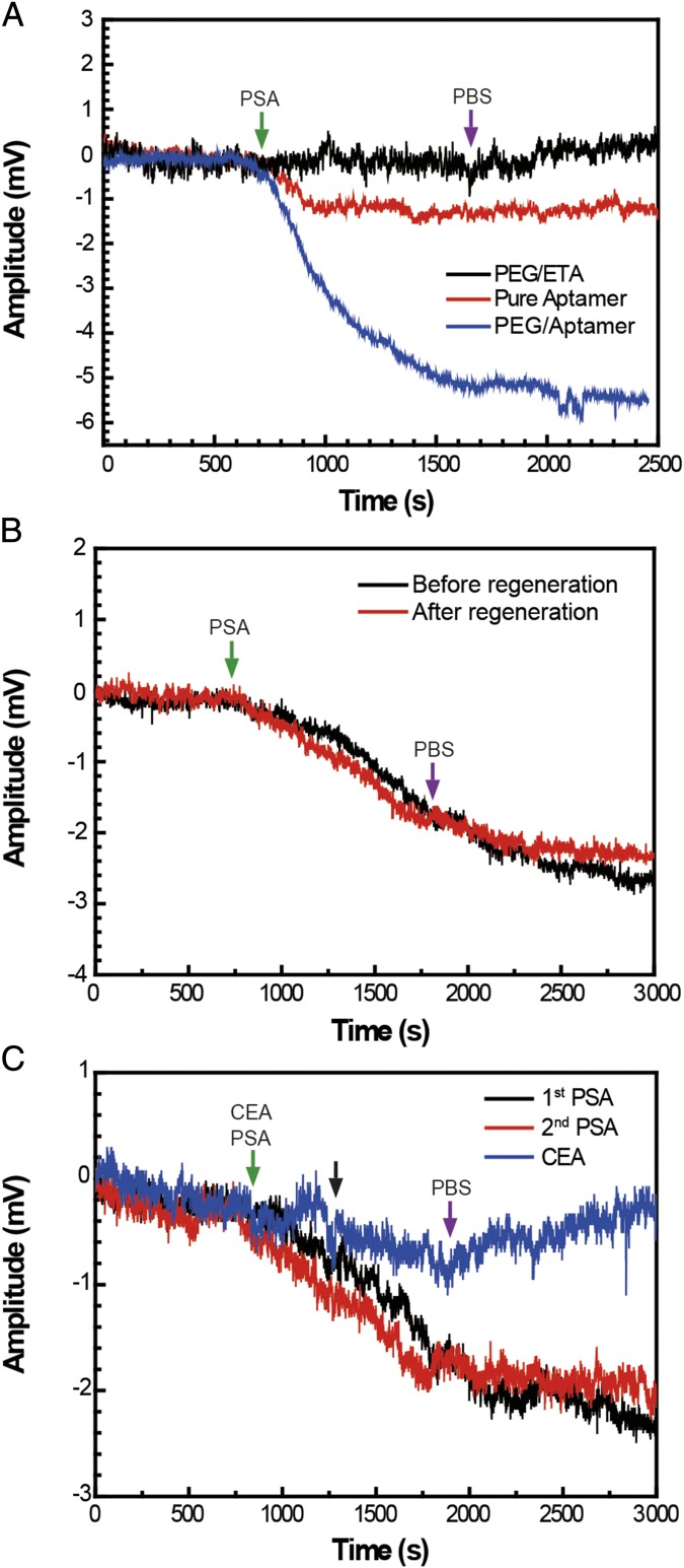
Last, we have investigated specific detection of PSA using graphene devices comodified with PEG and a DNA aptamer for PSA (Materials and Methods). The DNA aptamer is advantageous as the receptor for several reasons, including (i) the conformational changes of highly charged aptamer upon protein binding (37, 38) can result in a significant change in electric field near the sensor surface even if the solution pH is close to the protein pI, and (ii) the aptamer can be denatured and refolded multiple times without loss of activity (39, 40) for multiple experiments. All experiments were carried out in pH 7.4 1× PBS containing 2 mM Mg2+, where the added Mg2+ helps to maintain the active aptamer conformation before and after regeneration (39, 41). Notably, sensing experiments carried out with 1:2 PEG:aptamer-comodified graphene FET devices (blue curve, Fig. 4A) showed a well-defined 5.2 mV irreversible response to 300 nM PSA, which contrasts the response of the PEG/ETA control device (black curve, Fig. 4A) that exhibited no measurable response. The absence of obvious response in the control device is consistent with the fact that these specific sensing experiments are carried out at physiological pH (vs. pH 6 in Fig. 3), which is close to (vs. lower than) the pI of PSA (34). In control experiments carried out with pure aptamer-modified devices (red curve, Fig. 4A), there was a ∼1.2 mV irreversible response. This latter sensor response is almost five times smaller than that obtained with the 1:2 PEG:aptamer-modified devices, and thus supports the importance of the PEG layer for increasing the effective Debye length and sensitivity of the comodified graphene FET sensors.
Fig. 4.
Specific PSA detection in high–ionic-strength solutions. (A) The 300 nM PSA responses from 1:2 PEG:ETA-, pure aptamer-, and 1:2 PEG:aptamer-modified graphene FET devices. (B) A device with 1:2 PEG:aptamer modification shows consistent response to 100 nM PSA before and after 6 M guanidinium chloride regeneration for 10 min. (C) A device (distinct from B) with 1:2 PEG:aptamer modification first shows consistent response to 100 nM PSA before and after regeneration, and then shows a weaker and reversible response to 100 nM CEA. All experiments were carried out in pH 7.4 1× PBS containing 2 mM Mg2+.
Given the strong aptamer/PSA binding, we have investigated regeneration of the active receptor by denaturing the aptamer with guanidinium chloride (40). For example, following initial detection of 100 nM PSA (black curve, Fig. 4 B and C), devices were treated with 6 M guanidinium chloride for 10 min and then washed in the pH 7.4 buffer. Subsequent detection of the same concentration of PSA with the same devices (red curve, Fig. 4 B and C) showed equivalent sensing signal and confirmed that the functional aptamer was regenerated. In addition, we note that the amplitude of these signals, ∼2.3 mV, is approximately two times smaller than the higher concentration PSA measurement in Fig. 4A, indicating the potential for concentration-dependent detection. Finally, following a second cycle of regeneration, the data in Fig. 4C show that the device with carcinoembryonic antigen (CEA), which does not bind specifically to the aptamer, yielded a small (near-baseline) ∼0.5 mV reversible binding signal (blue curve, Fig. 4C) in contrast to the irreversible five times larger signal obtained for PSA at the same concentration. Together, these results show the capability to achieve specific real-time detection of proteins in physiological solution in competition with other proteins.
Conclusions
We have demonstrated a general strategy to enable direct FET sensing measurements in high–ionic-strength physiological solutions that involves comodification of device surfaces with PEG and spacer molecules or PEG and aptamer receptors. Concentration-dependent measurements made with PEG/ETA-modified graphene FET devices exhibited real-time reversible detection of PSA from 1 to 1,000 nM in 100 mM PB, which has a screening length comparable to physiological solutions, and further showed that detection was possible even at 150 mM PB. In addition, studies carried out using PEG/DNA aptamer-modified graphene devices showed irreversible specific binding and detection of PSA in pH 7.4 1× PBS solutions, whereas control experiments with CEA protein, which does not bind specifically to the aptamer, showed smaller reversible signals. In addition, the active aptamer receptor of the modified graphene devices could be regenerated to yield multiuse selective PSA sensing under these physiological conditions. We believe this work represents a critical step toward general application of nanomaterial-based FET sensors in many areas, including in vitro and in vivo real-time chip-based monitoring of disease marker proteins, which could have substantial impact on both fundamental research and health care, as well as integration in free-standing nanoelectronic scaffolds for engineered tissues and in vivo implants (42).
Materials and Methods
Graphene Synthesis.
Monolayer graphene was synthesized on 25-μm-thick Cu foil (Alfa Aesar) via a reported low-pressure CVD method (29). Before growth, the Cu foil was electropolished in phosphoric acid [85% (wt/wt)] and ethylene glycol [15% (wt/wt)] for 30 min and rinsed in deionized (DI) water. The polished Cu foil was loaded into a 1-inch quartz tube furnace, annealed in 40 sccm H2 during the 40-min room temperature-to-1,000 °C heating process, followed by a 20-min anneal at 1,000 °C. Graphene growth was initiated by introducing 5 sccm methane into furnace, and growth was continued for 30 min.
FET Sensor Fabrication.
Graphene films were transferred onto Si wafer using a reported poly(methyl methacrylate) (PMMA) method (29), where PMMA (PMMA-C5; Microchem) was spin-coated (PWM2; Headway Research, Inc.) on as-grown graphene/Cu foil, at 2,000 rpm for 1 min, the Cu foil was etched in ammonium persulfate aqueous solution [10% (wt/wt)], the floating PMMA/graphene film was rinsed in DI water, and then transferred to the SiO2 surface of Si/SiO2 target wafer. PMMA was dissolved in acetone at 70 °C.
The graphene was patterned using photolithography. (i) LOR 3A (Microchem) was spin-coated onto graphene/Si wafer, at 4,000 rpm for 1 min, followed by 180 °C baking for 2 min. S1805 (Microchem) was spin-coated on the wafer at 4,000 rpm for 1 min, followed by 1 min of 115 °C baking. (ii) Graphene channels were defined by photolithography. (iii) After developing in CD-26 (Microchem) for 1 min, the graphene/Si wafer was placed into an O2 plasma cleaner (Fetmo; Diener Electronic) to etch graphene in regions without photoresist protection. (iv) Photoresist on the graphene/Si wafer was removed in Remover PG (Microchem). (v) The patterned graphene was further cleaned by vacuum thermal annealing at 300 °C for 1 h (Jipelec rapid thermal processor; SEMCO Technologies) to reduce PMMA residue (43).
Device fabrication was completed by combination of photolithography with metal and Si3N4 deposition. (i) LOR 3A (Microchem) was spin-coated onto graphene/Si wafer, at 4,000 rpm for 1 min, followed by 180 °C baking for 2 min. S1805 (Microchem) was subsequently coated on top, at 4,000 rpm for 1 min, followed by 1 min 115 °C baking. (ii) Metal contacts were defined using photolithography. (iii) After developing in CD-26 for 1 min, 10-nm Cr/65-nm Au/3-nm Cr were deposited via thermal evaporation, with deposition rates of 0.2, 2.0, and 1 Å/s, respectively. (iv) A 30-nm Si3N4 passivation layer was deposited over the metal contacts via magnetron sputtering (Orion 3; AJA International).
Electrical Characterization.
Devices chips were wire-bonded to a PCB interface board as shown in Fig. 1B, and then a PDMS microfluidic channel was mounted on the sensor chip with the channel aligned with the central region of the device chip where the graphene FETs are located. Polyethylene tubing was attached to the inlet and the outlet holes on the PDMS microfluidic channel, and buffer or protein/buffer solutions were drawn through the channel using a syringe pump.
Water-gate versus conductance measurements were carried out in 1× PBS using a home-made probe station. The water gate was varied at 100 mV/s sweep rate while monitoring the graphene FET conductance for a fixed 100 mV source/drain voltage; the FET conductance was amplified (1211; DL Instruments). The resulting conductance versus water-gate curves are used to calculate CNP and transconductance values for the devices.
Depending on the integrity of transferred graphene film, the yield of working sensors (showing water-gate response) calculated based on all of 180 available source/drain electrodes on each sensor chip was usually above 95%.
AFM Characterization.
The device chip was mounted in an airtight chamber, before being immersed in a droplet of 1× PBS, and measurements were carried out at room temperature using an AFM (MFP-3D Coax AFM; Oxford Instruments Asylum Research). A Si AFM tip (AC160TS-R3-35; Oxford Instruments Asylum Research) was used to acquire both AFM height and amplitude images of graphene channel, under constant amplitude tapping (AC) mode.
Surface Modification.
The device chip was soaked in 0.6 mM PYCOOH (Sigma-Aldrich) in dimethylformamide (DMF) (Sigma-Aldrich) solution for 1 h. After washing with DMF three times, the device chip was immersed in pure DMF for 1 h at 60 °C with agitation to further remove excess PYCOOH. Then, the device chip was modified with ETA (411000; Sigma-Aldrich), pure aptamer, the mixture of 10-kDa PEG (PSB-267; Creative PEGWorks) and ETA, or PEG and aptamer (5′-NH2-C6-TTTTTAATTAAAGCTCGCCATCAAATAGCTTT-3′; Gene Link) using EDC (03449; Sigma-Aldrich) and N-hydroxysulfosuccinimide sodium salt (56485; Sigma-Aldrich) cross-linkers (28). For the ETA and PEG/ETA-modified graphene devices, the functionalization was carried out in a Petri dish on a shaker for 2 h, followed by rinsing with DI water. For pure aptamer and PEG/aptamer and the corresponding ETA/PEG (control)-modified graphene devices, the functionalization was conducted in the PDMS microfluidic channel for 1.5 h, followed by rinsing with pH 7.4 1× PBS buffer containing 2 mM Mg2+.
Aptamer Regeneration.
To release PSA and regenerate the aptamer receptors, the device chip was incubated with 6 M guanidinium chloride (G3272; Sigma-Aldrich) for 10 min, followed by DI water wash and then PBS (containing 2 mM Mg2+) buffer to reconstitute the functional conformation of PSA aptamers.
Sensing Measurements.
Measurements were carried out using up to three independent lock-in amplifiers (SR830; Stanford Research Systems) with 30 mV modulation amplitudes and modulation frequencies of 79, 97, and 103 Hz to simultaneously record three graphene devices selected from 180 devices on the chip. An Ag/AgCl electrode was used as a reference; sensing experiments were all carried out in the linear regime, which in some cases required a DC offset of the water-gate/reference voltage. The conductance versus time data were digitized and recorded on computer using custom software. The water-gate responses of devices were characterized before PSA detection experiments, and device transconductance values were determined from the water-gate data. Graphene FET signals were converted to absolute millivolt values for the calibrated sensing signals using the device transconductance determined from these water-gate measurements.
SI Text
Raman Characterization of Graphene Before and After Modification.
Raman spectroscopy is widely used to characterize the quality and doping level of graphene films (30). In this work, Raman spectra were obtained from graphene sheets before/after pyrene butyric acid (PYCOOH) and polyethylene glycol (PEG) modification steps (see detailed modification procedures in Materials and Methods) in air (Fig. S2). A typical Raman spectrum of bare graphene transferred to a SiO2/Si substrate used for device fabrication (Fig. S2A) shows features representative of a high-quality graphene monolayer, including negligible D peak at ∼1,350 cm−1, narrow 2D peak at ∼2,680 cm−1 (FWHM = 43 cm−1) and a 2D-to-G intensity ratio, I2D/IG, of >2. Quantifying the I2D/IG ratio from 2D maps of representative 10 × 10-μm2 areas yields an average ±1 SD of 3.6 ± 0.5, which is consistent with monolayer graphene (30).
In addition, 2D maps of the graphene G-band shift measured from 10 × 10-μm2 graphene regions before and after PYCOOH and PEG modification steps (Fig. S2B), yield a significant downshift in the average values from 1,594 to 1,591 and then to 1,585 cm−1, respectively. Previous work has shown that the Raman G peak, which corresponds to the E2g phonon at the Brillouin zone center, will stiffen with p-type and soften with n-type doping, leading to upshifts or downshifts in Raman spectra (44). Pristine undoped monolayer graphene shows a G band at 1,584 cm−1, whereas the G band of the bare graphene measured in our experiment, 1,592 cm−1, indicates a substrate-induced p-doping effect (45). Both PYCOOH and PEG modifications lead to electron or n-type doping, resulting in the observed downshift of the G band. In comparison, the CNP measurements (Fig. 2C), which were carried out in pH 7.4 1× PBS, show the same overall effect from bare to PEG-modified graphene devices with a 0.55 ± 0.08 to 0.22 ± 0.06 V shift that is consistent with n-type doping (33). The initial modification step with PYCOOH does not show a statistically significant CNP change, 0.55 ± 0.08 to 0.62 ± 0.07 (Fig. 2C), although this difference compared with dry-state Raman can be attributed to deprotonation of the PYCOOH carboxylic acid group in 1× PBS used for the electrical measurements.
Estimate of PEG Layer Dielectric Constant.
The PEG modification layer adds a hydrated dielectric polymer layer on graphene, and thus the overall interfacial capacitance of the PEG modified graphene devices is composed of graphene quantum capacitance (Cq) and PEG-induced capacitance (CPEG) in series (46), shown as Eq. S1:
| [S1] |
Cq for bare graphene, ∼7 μF/cm2, and the overall interfacial capacitance in 100 mM NaCl (pH 7) solution, ∼5 μF/cm2, have been reported previously (46). Because the interfacial capacitance is proportional to the transconductance of FET devices (47), the values measured in Fig. 3D for bare and PEG-modified graphene yield an estimated CPEG of ∼4.2 μF/cm2. Given the thickness of PEG measured by AFM (Fig. 2A), ∼6 nm, the dielectric constant of PEG layer, εr,PEG, estimated using Eq. S2,
| [S2] |
is 28, where CPEG is the capacitance of the PEG layer, ε0 is the electric constant, and dPEG is the PEG layer thickness. Reported measurements of the dielectric constant of PEG in aqueous solution show a monotonic decrease with increasing PEG concentration, and thus our estimated value lies between dehydrated PEG, 11.8, and water, ∼80 (48). Our analysis suggests that the PEG layer on the graphene devices is partially hydrated in buffer solution and consistent with our hypothesis, although future work will be needed to fully characterize the properties of the PEG layers.
Acknowledgments
C.M.L. acknowledges support from the Defense Threat Reduction Agency through the US Naval Research Laboratory and the Air Force Office of Scientific Research. This work was performed in part at the Harvard University Center for Nanoscale Systems, a member of the National Nanotechnology Coordinated Infrastructure Network, which is supported by the National Science Foundation.
Footnotes
The authors declare no conflict of interest.
This article contains supporting information online at www.pnas.org/lookup/suppl/doi:10.1073/pnas.1625010114/-/DCSupplemental.
References
- 1.Zhang A, Lieber CM. Nano-bioelectronics. Chem Rev. 2016;116(1):215–257. doi: 10.1021/acs.chemrev.5b00608. [DOI] [PMC free article] [PubMed] [Google Scholar]
- 2.Patolsky F, Zheng G, Lieber CM. Nanowire sensors for medicine and the life sciences. Nanomedicine (Lond) 2006;1(1):51–65. doi: 10.2217/17435889.1.1.51. [DOI] [PubMed] [Google Scholar]
- 3.Balasubramanian K, Kern K. 25th anniversary article: Label-free electrical biodetection using carbon nanostructures. Adv Mater. 2014;26(8):1154–1175. doi: 10.1002/adma.201304912. [DOI] [PubMed] [Google Scholar]
- 4.Kauffman DR, Star A. Electronically monitoring biological interactions with carbon nanotube field-effect transistors. Chem Soc Rev. 2008;37(6):1197–1206. doi: 10.1039/b709567h. [DOI] [PubMed] [Google Scholar]
- 5.Liu Y, Dong X, Chen P. Biological and chemical sensors based on graphene materials. Chem Soc Rev. 2012;41(6):2283–2307. doi: 10.1039/c1cs15270j. [DOI] [PubMed] [Google Scholar]
- 6.Yin PT, Shah S, Chhowalla M, Lee KB. Design, synthesis, and characterization of graphene-nanoparticle hybrid materials for bioapplications. Chem Rev. 2015;115(7):2483–2531. doi: 10.1021/cr500537t. [DOI] [PMC free article] [PubMed] [Google Scholar]
- 7.Cui Y, Wei Q, Park H, Lieber CM. Nanowire nanosensors for highly sensitive and selective detection of biological and chemical species. Science. 2001;293(5533):1289–1292. doi: 10.1126/science.1062711. [DOI] [PubMed] [Google Scholar]
- 8.Zheng G, Patolsky F, Cui Y, Wang WU, Lieber CM. Multiplexed electrical detection of cancer markers with nanowire sensor arrays. Nat Biotechnol. 2005;23(10):1294–1301. doi: 10.1038/nbt1138. [DOI] [PubMed] [Google Scholar]
- 9.Stern E, et al. Label-free immunodetection with CMOS-compatible semiconducting nanowires. Nature. 2007;445(7127):519–522. doi: 10.1038/nature05498. [DOI] [PubMed] [Google Scholar]
- 10.Chen RJ, et al. Noncovalent functionalization of carbon nanotubes for highly specific electronic biosensors. Proc Natl Acad Sci USA. 2003;100(9):4984–4989. doi: 10.1073/pnas.0837064100. [DOI] [PMC free article] [PubMed] [Google Scholar]
- 11.Hahm J-i, Lieber CM. Direct ultrasensitive electrical detection of DNA and DNA sequence variations using nanowire nanosensors. Nano Lett. 2004;4(1):51–54. [Google Scholar]
- 12.Star A, et al. Label-free detection of DNA hybridization using carbon nanotube network field-effect transistors. Proc Natl Acad Sci USA. 2006;103(4):921–926. doi: 10.1073/pnas.0504146103. [DOI] [PMC free article] [PubMed] [Google Scholar]
- 13.Mohanty N, Berry V. Graphene-based single-bacterium resolution biodevice and DNA transistor: Interfacing graphene derivatives with nanoscale and microscale biocomponents. Nano Lett. 2008;8(12):4469–4476. doi: 10.1021/nl802412n. [DOI] [PubMed] [Google Scholar]
- 14.Patolsky F, et al. Electrical detection of single viruses. Proc Natl Acad Sci USA. 2004;101(39):14017–14022. doi: 10.1073/pnas.0406159101. [DOI] [PMC free article] [PubMed] [Google Scholar]
- 15.Wang WU, Chen C, Lin KH, Fang Y, Lieber CM. Label-free detection of small-molecule-protein interactions by using nanowire nanosensors. Proc Natl Acad Sci USA. 2005;102(9):3208–3212. doi: 10.1073/pnas.0406368102. [DOI] [PMC free article] [PubMed] [Google Scholar]
- 16.Duan X, et al. Quantification of the affinities and kinetics of protein interactions using silicon nanowire biosensors. Nat Nanotechnol. 2012;7(6):401–407. doi: 10.1038/nnano.2012.82. [DOI] [PMC free article] [PubMed] [Google Scholar]
- 17.Lin T-W, et al. Label-free detection of protein-protein interactions using a calmodulin-modified nanowire transistor. Proc Natl Acad Sci USA. 2010;107(3):1047–1052. doi: 10.1073/pnas.0910243107. [DOI] [PMC free article] [PubMed] [Google Scholar]
- 18.Stern E, et al. Importance of the Debye screening length on nanowire field effect transistor sensors. Nano Lett. 2007;7(11):3405–3409. doi: 10.1021/nl071792z. [DOI] [PMC free article] [PubMed] [Google Scholar]
- 19.Israelachvili JN. Intermolecular and Surface Forces: With Applications to Colloidal and Biological Systems. Academic; London: 1985. [Google Scholar]
- 20.Stern E, et al. Label-free biomarker detection from whole blood. Nat Nanotechnol. 2010;5(2):138–142. doi: 10.1038/nnano.2009.353. [DOI] [PMC free article] [PubMed] [Google Scholar]
- 21.Elnathan R, et al. Biorecognition layer engineering: Overcoming screening limitations of nanowire-based FET devices. Nano Lett. 2012;12(10):5245–5254. doi: 10.1021/nl302434w. [DOI] [PubMed] [Google Scholar]
- 22.Maehashi K, et al. Label-free protein biosensor based on aptamer-modified carbon nanotube field-effect transistors. Anal Chem. 2007;79(2):782–787. doi: 10.1021/ac060830g. [DOI] [PubMed] [Google Scholar]
- 23.Kulkarni GS, Zhong Z. Detection beyond the Debye screening length in a high-frequency nanoelectronic biosensor. Nano Lett. 2012;12(2):719–723. doi: 10.1021/nl203666a. [DOI] [PubMed] [Google Scholar]
- 24.Kulkarni GS, Zang W, Zhong Z. Nanoelectronic heterodyne sensor: A new electronic sensing paradigm. Acc Chem Res. 2016;49(11):2578–2586. doi: 10.1021/acs.accounts.6b00329. [DOI] [PubMed] [Google Scholar]
- 25.Gao N, et al. General strategy for biodetection in high ionic strength solutions using transistor-based nanoelectronic sensors. Nano Lett. 2015;15(3):2143–2148. doi: 10.1021/acs.nanolett.5b00133. [DOI] [PMC free article] [PubMed] [Google Scholar]
- 26.Chen RJ, Zhang Y, Wang D, Dai H. Noncovalent sidewall functionalization of single-walled carbon nanotubes for protein immobilization. J Am Chem Soc. 2001;123(16):3838–3839. doi: 10.1021/ja010172b. [DOI] [PubMed] [Google Scholar]
- 27.Wang X, Tabakman SM, Dai H. Atomic layer deposition of metal oxides on pristine and functionalized graphene. J Am Chem Soc. 2008;130(26):8152–8153. doi: 10.1021/ja8023059. [DOI] [PubMed] [Google Scholar]
- 28.Hermanson GT. Bioconjugate Techniques. 3rd Ed Elsevier; London: 2013. [Google Scholar]
- 29.Li X, et al. Transfer of large-area graphene films for high-performance transparent conductive electrodes. Nano Lett. 2009;9(12):4359–4363. doi: 10.1021/nl902623y. [DOI] [PubMed] [Google Scholar]
- 30.Ferrari AC, et al. Raman spectrum of graphene and graphene layers. Phys Rev Lett. 2006;97(18):187401. doi: 10.1103/PhysRevLett.97.187401. [DOI] [PubMed] [Google Scholar]
- 31.Lenski DR, Fuhrer MS. Raman and optical characterization of multilayer turbostratic graphene grown via chemical vapor deposition. J Appl Phys. 2011;110(1):013720. [Google Scholar]
- 32.Pasche S, Textor M, Meagher L, Spencer ND, Griesser HJ. Relationship between interfacial forces measured by colloid-probe atomic force microscopy and protein resistance of poly(ethylene glycol)-grafted poly(l-lysine) adlayers on niobia surfaces. Langmuir. 2005;21(14):6508–6520. doi: 10.1021/la050386x. [DOI] [PubMed] [Google Scholar]
- 33.Liu HT, Liu YQ, Zhu DB. Chemical doping of graphene. J Mater Chem. 2011;21(10):3335–3345. [Google Scholar]
- 34.Wang MC, et al. Prostate antigen: A new potential marker for prostatic cancer. Prostate. 1981;2(1):89–96. doi: 10.1002/pros.2990020109. [DOI] [PubMed] [Google Scholar]
- 35.Armbruster DA. Prostate-specific antigen: Biochemistry, analytical methods, and clinical application. Clin Chem. 1993;39(2):181–195. [PubMed] [Google Scholar]
- 36.Levine IN. Physical Chemistry. 6th Ed McGraw-Hill; Boston: 2009. [Google Scholar]
- 37.Jiang Y, Fang X, Bai C. Signaling aptamer/protein binding by a molecular light switch complex. Anal Chem. 2004;76(17):5230–5235. doi: 10.1021/ac049565u. [DOI] [PubMed] [Google Scholar]
- 38.Yang CJ, Jockusch S, Vicens M, Turro NJ, Tan W. Light-switching excimer probes for rapid protein monitoring in complex biological fluids. Proc Natl Acad Sci USA. 2005;102(48):17278–17283. doi: 10.1073/pnas.0508821102. [DOI] [PMC free article] [PubMed] [Google Scholar]
- 39.Liss M, Petersen B, Wolf H, Prohaska E. An aptamer-based quartz crystal protein biosensor. Anal Chem. 2002;74(17):4488–4495. doi: 10.1021/ac011294p. [DOI] [PubMed] [Google Scholar]
- 40.Xiao Y, Lai RY, Plaxco KW. Preparation of electrode-immobilized, redox-modified oligonucleotides for electrochemical DNA and aptamer-based sensing. Nat Protoc. 2007;2(11):2875–2880. doi: 10.1038/nprot.2007.413. [DOI] [PubMed] [Google Scholar]
- 41.Hennelly SP, Novikova IV, Sanbonmatsu KY. The expression platform and the aptamer: Cooperativity between Mg2+ and ligand in the SAM-I riboswitch. Nucleic Acids Res. 2013;41(3):1922–1935. doi: 10.1093/nar/gks978. [DOI] [PMC free article] [PubMed] [Google Scholar]
- 42.Fu T-M, et al. Stable long-term chronic brain mapping at the single-neuron level. Nat Methods. 2016;13(10):875–882. doi: 10.1038/nmeth.3969. [DOI] [PubMed] [Google Scholar]
- 43.Pirkle A, et al. The effect of chemical residues on the physical and electrical properties of chemical vapor deposited graphene transferred to SiO2. Appl Phys Lett. 2011;99:122108. [Google Scholar]
- 44.Pisana S, et al. Breakdown of the adiabatic Born-Oppenheimer approximation in graphene. Nat Mater. 2007;6(3):198–201. doi: 10.1038/nmat1846. [DOI] [PubMed] [Google Scholar]
- 45.Shi YM, Dong XC, Chen P, Wang JL, Li LJ. Effective doping of single-layer graphene from underlying SiO2 substrates. Phys Rev B. 2009;79(11):115402. [Google Scholar]
- 46.Chen S, et al. A graphene field-effect capacitor sensor in electrolyte. Appl Phys Lett. 2012;101(15):154106. [Google Scholar]
- 47.Moon JS, et al. Top-gated epitaxial graphene FETs on Si-face SiC wafers with a peak transconductance of 600 mS/mm. Ieee Electr Device L. 2010;31(4):260–262. [Google Scholar]
- 48.Arnold K, Herrmann A, Pratsch L, Gawrisch K. The dielectric properties of aqueous solutions of poly(ethylene glycol) and their influence on membrane structure. Biochim Biophys Acta. 1985;815(3):515–518. doi: 10.1016/0005-2736(85)90381-5. [DOI] [PubMed] [Google Scholar]


