Abstract
The facet‐engineered surface and interface design for photocatalytic materials has been proven as a versatile approach to enhance their photocatalytic performance. This review article encompasses some recent advances in the facet engineering that has been performed to control the surface of mono‐component semiconductor systems and to design the surface and interface structures of multi‐component heterostructures toward photocatalytic applications. The review begins with some key points which should receive attention in the facet engineering on photocatalytic materials. We then discuss the synthetic approaches to achieve the facet control associated with the surface and interface design. In the following section, the facet‐engineered surface design on mono‐component photocatalytic materials is introduced, which forms a basis for the discussion on more complex systems. Subsequently, we elucidate the facet‐engineered surface and interface design of multi‐component photocatalytic materials. Finally, the existing challenges and future prospects are discussed.
Keywords: facets, surfaces, interfaces, photocatalysis, solar energy
1. Introduction
To alleviate the global energy crisis and environmental pollution, the photocatalysis that directly converts solar light into chemical energy has been widely explored over the past decades.1, 2, 3 As commonly recognized, the invention of photocatalysts with high activity, selectivity and stability is the prerequisite for putting “photocatalysis” into use in industry and in our lives.4, 5, 6 To achieve this goal, semiconductor materials with well‐defined sizes, structures, compositions and shapes have been extensively developed as photocatalysts for various reactions including water splitting, CO2 reduction and pollutant degradation.7, 8, 9 In particular, size shrinkage not only boosts the number of catalytic sites, but also may tailor the electronic structures of catalysts, which highlights the niches of photocatalytic materials at the microscale or nanoscale. The well‐defined parameters set up a platform for understanding their correlations with photocatalytic performance, allowing maneuvering the performance through parameter adjustment.10
During a typical photocatalytic process, charge kinetics plays a central role in the conversion of solar to chemical energy through generating and transferring charge carriers. In principle, three basic steps are involved in such a complex process in terms of charge kinetics: 1) charge generation under semiconductor photoexcitation; 2) charge transfer to catalyst surface; and 3) charge consumption in redox reactions on the catalyst surface.11 The efficiency of each step largely determines the overall performance of a photocatalyst. Thus it is imperative to facilitate and reconcile the steps for the improved solar‐to‐chemical energy conversion. In efforts to achieve this goal, the photocatalytic materials have been developed from bare semiconductors to multi‐component hybrid structures in recent years.12, 13 In the hybrid photocatalysts, the synergism between different components has been proven to extend light absorption range in charge generation, to reduce electron‐hole recombination in charge transfer, or to improve reactant adsorption and activation in charge consumption.11 The synergism relies on the surface and interface structures of hybrid photocatalysts, thereby holding the promise for optimizing photocatalytic performance.13, 14 The surface where the redox reactions take place has a huge impact on the efficiency of reaction molecules receiving the photogenerated charges toward product generation. This importance to surface reactions is generally applied to both bare semiconductors and hybrid structures. In the hybrid structures, an additional important parameter is the interface between two adjacent components where charge carriers are transferred. The structure and quality of interfaces hold the key to the performance of charge transfer from light‐harvesting component to reaction sites and between different light‐harvesting centers. Taken together, the structures of surface and interface should be tightly controlled to fully functionalize the multiple‐component material systems.
To control the surface and interface structures, the facets for forming the surface and interface are the key parameters that should be rationally selected. The facets exposed on photocatalyst surface may affect the photocatalytic performance through various working mechanisms. For instance, 1) surface atomic arrangements determine the adsorption and activation of reaction molecules, tuning catalytic activity and selectivity (Figure 1 a);15, 16 2) the surface electronic band structures (i.e., surface states), which depend on surface facets, would provide the photogenerated charge carriers with tunable redox abilities for catalytic reactions (Figure 1b);17 3) the efficiency of charge separation and transfer inside light‐harvesting semiconductors depends on crystal orientations, resulting in the varied charge densities for surface reactions.18, 19 Moreover, when the semiconductor is enclosed by multiple facets, the varied electronic band structures of surface facets may result in the spatial charge separation which accumulates the photogenerated electrons and holes on different facets for reduction and oxidation reaction, respectively (Figure 1c).20
Figure 1.
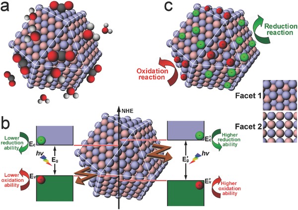
Schematics illustrating the important roles of facets in the surface design of photocatalytic materials. a) Adsorption and activation of reactant molecules on different facets. b) Redox abilities of photogenerated charge carriers tuned by the surface electronic band structures of different facets. c) Accumulations of photogenerated electrons or holes on different facets.
As compared with bare semiconductors, the multi‐component systems are more complicated as the interfaces between the components become involved. The component facets that form the interfaces via solid‐solid contact may impact on interfacial charge transfer from several aspects. For instance, 1) interfacial charge transfer takes place after the charge carriers are transported from bulk to the interface, so the facet‐dependent charge accumulation as described above would maneuver the charge transfer (Figure 2 a);20 2) the interfacial alignment of the energy bands that are strongly correlated with component facets determines the potential difference for driving interfacial charge transfer (Figure 2b);21 3) the electronic coupling and defect density at the interface, depending on the compatibility of facet structures, largely affect the efficiency of charge transfer across the interface (Figure 2c).22 From the statements above, one can identify that highly efficient photocatalytic materials would be designed by tailoring the exposed facet on surface and the contact facets at interface.
Figure 2.
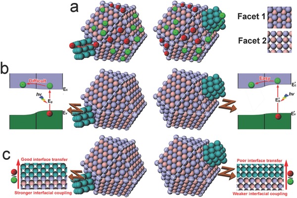
Schematics illustrating the important roles of facets in the interface design of photocatalytic hybrid materials. a) Interfacial charge transfer following the accumulation of photogenerated electrons or holes on different facets. b) Interfacial charge transfer efficiency depending on the component energy bands which are correlated their surface facets. c) Interfacial charge transfer relying on the structural and electronic couplings of components which vary with facet contacts.
To date, the advanced synthetic approaches to micro‐ and nanomaterials with well‐defined facets have significantly promoted the development of facet‐engineered surface and interface design in photocatalysis. The precisely controlled photocatalysts offer an ideal platform for investigating the dependence of photocatalytic performance on facets and the related mechanisms.23, 24, 25, 26 In this review, we focus on the recent advances in the facet‐engineered surface and interface design toward the photocatalysis applications. The review will begin with some key points which should receive attention in the facet‐engineered surface and interface design on photocatalytic materials. We will then discuss the synthetic approaches to realizing the facet control toward the surface and interface design of photocatalytic materials. In the following section, the facet‐engineered surface design on single‐component photocatalytic materials will be introduced. Subsequently, we will elucidate the facet‐engineered surface and interface design of multi‐component photocatalytic materials, respectively. Finally, the existing challenges and future prospects will be discussed.
2. Key Points to the Facet‐Engineered Surface and Interface Design
Engineering the facets at the locations of surface and interface is a challenging task in the design of photocatalytic materials. Prior to the following discussions, some key points to the facet‐engineered surface and interface design should be clarified.
-
1)
The aim of this facet engineering is to enhance photocatalytic performance through rationally tailoring the surface and interface structures of photocatalysts. To reliably reflect the relationship between facets and photocatalytic performance, other parameters of the photocatalytic materials such as chemical compositions and crystal structures should be kept constant in control experiments. For this reason, the advanced synthetic protocols with high controllability over the parameters are required to exclude the interference from other parameter variations in the facet‐dependent studies.
-
2)
The facet engineering on mono‐component photocatalytic materials (i.e., bare semiconductors) is relatively simple, as facet adjustment is only needed for the surface of light‐harvesting components. In comparison, the facet engineering on the photocatalytic hybrid structures is dramatically complicated as the involvement of multiple components leads to the increased number of surfaces as well as the formation of interface between the components. It should be noted that in some hybrid photocatalysts, certain surfaces do not serve as the catalytic active sites while some interfaces do not provide channels for charge carrier transportation. These possibilities make their facet adjustment unable to maneuver charge kinetics and to enhance photocatalytic performance. Thus the rational design on suitable surfaces and interfaces is highly important to the facet engineering.
-
3)
In a hybrid structure, the structural correlation of surface with interface should be taken into account during the facet adjustment. For instance, when an interface is formed on the given component surface, the interfacial structure will inherit from the surface facet of this component. For this reason, controlling the exposed facet of an existing component inevitably results in variations in the facet structure of interface.
From the analysis above, one can envision that engineering the facets at the surface and interface of a hybrid structure would be a grand challenge. It not only calls for the advanced synthetic techniques with high precision (e.g., at the atomic level), but also requires high rationality for the intrinsic correlation of surface with interface and the relationship between structural characteristics and functionality.
3. Synthetic Approaches to Facet Control toward Surface and Interface Design
3.1. Facet Control on the Surface of Mono‐Component Photocatalytic Materials
For mono‐component structures, light‐harvesting semiconducors are the most widely used photocatalytic materials, and the facet engineering mainly focuses on their surface. Over the past decade, various synthetic approaches have been developed to control the exposed facets of photocatalytic semiconductor materials, including use of facet‐selective capping agents, kinetic control, thermodynamic control, and selective etching based on crystal anisotropy.
Capping agents have been extensively employed to manuever the facet growth of micro‐ and nanomaterials.27, 28 The capping agents can be selectively adsorbed to specific facets so as to suppress the growth along their axes. As a result, the facet with a slower growth rate will be more exposed on the surface. By increasing the amount of capping agent, the ratio of various facets can be tailored to ultimately leave the capped facet dominant on surface. For instance, the exposed facets of Cu2O were tailored by simply altering the amount of added poly(vinyl pyrrolidone) (PVP).29 In the absence of PVP, cubic Cu2O microcrystals enclosed with six {100} planes were obtained (Figure 3 a). The addition of PVP into the synthetic system resulted in the exposure of {111} surface as the preferential adsorption of PVP to the Cu2O{111} facets could hinder their growth (Figure 3b). The simultaneous {100} shrinkage and {111} enlargement on surface, enabled by the increase of PVP concentrations, led to the shape evolution from corner‐truncated cubes to cubooctahedrons and eventually to the highly symmetric octahedrons fully covered by {111} planes (Figure 3a,b).
Figure 3.
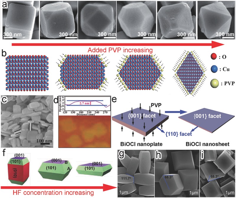
a) Scanning electron microscopy (SEM) images showing the evolution of Cu2O polyhedrons from cubes to octahedrons through increasing the amount of added PVP. b) Schematics illustrating the mechanism involved in the synthesis of Cu2O polyhedrons. Reproduced with permission.29 Copyright 2009, Royal Society of Chemistry. c) SEM image of the BiOCl nanoplates. d) Atomic force microscopy (AFM) image of ultrathin BiOCl nanosheets. e) Schematics illustrating the mechanism involved in the synthesis of 2D BiOCl nanostructures. Reproduced with permission.30 Copyright 2013, American Chemical Society. f–i) Schematic illustration (f) and (g–i) SEM images of anatase TiO2 crystals formed through increasing HF concentrations. Reproduced with permission.32
Certainly the facet control by capping agents is not limited to the synthesis of symmetric polyhedral structures. This strategy has been validated for the formation of two‐dimensional (2D) photocatalytic materials that possess the high percentage of a single facet on their top and bottom flat surfaces. In a typical case, BiOCl nanoplates with thickness in ca. 30 nm and ultrathin nanosheets with thickness in ca. 2.7 nm were synthesized without and with PVP as capping agent, respectively (Figure 3c,d).30 The thickness shrinkage was attributed to the selective deposition of PVP on the top and bottom {001} planes, thereby preventing the axial growth (Figure 3e). As a result, the percentage of {001} planes increased from 62% in BiOCl nanoplates to 95% in ultrathin BiOCl nanosheets.
It should be noted that the polymeric capping agents would remain on the facets and influence the adsorption and activation of reactant molecules. This forms an obstacle for reliably evaluating the facet‐dependent photocatalytic performance. Small inorganic ions, alternative to organic surfactants and ligands, can be employed as the facet‐selective capping agents. This class of capping agents not only allows the access of reactants to the capped facets, but also can be more readily removed to obtain clean surface.31 Pan et al. employed F– as a facet‐controlling agent to successfully tailor the exposed facets of anatase TiO2.32 As the F– was selectively adsorbed to {001} planes, increasing the HF concentrations could inhibit the crystal growth along the [001] direction. As a result, the percentage of {001} planes on surface has been promoted from 14% to 24% and then to 40%, along with the shape evolution from columns to truncated bipyramids with different aspect ratios (Figure 3f–i). To the extreme, a further higher concentration of HF produced the TiO2 nanosheets dominated with {001} facet on the top and bottom surfaces as separately reported in another work.33
As demonstrated above, the facet control via capping agents can make the crystal growth deviated from the forms that are originally favored by thermodynamics.34 Kinetic control is another versatile approach to the thermodynamically disfavored surface facets.23 For instance, the exposed facets of Ag2O were tailored through altering the concentrations of starting materials.35 By lowering the concentrations of AgNO3 and NH3·H2O, the shapes of Ag2O crystals evolved from octahedrons bounded by {111} planes to truncated octahedrons by mixed {111}/{100} planes and then to cubes by {100} planes (Figure 4 a–c). In this case, the alteration of growth environments by reactant concentrations substantially manipulated the growth rates (R) of Ag2O along the [111] and [100] directions. At a sufficiently low reactant concentration, the ratio of R[111] to R[100] was increased to yield the cubic Ag2O crystals (Figure 4d).
Figure 4.
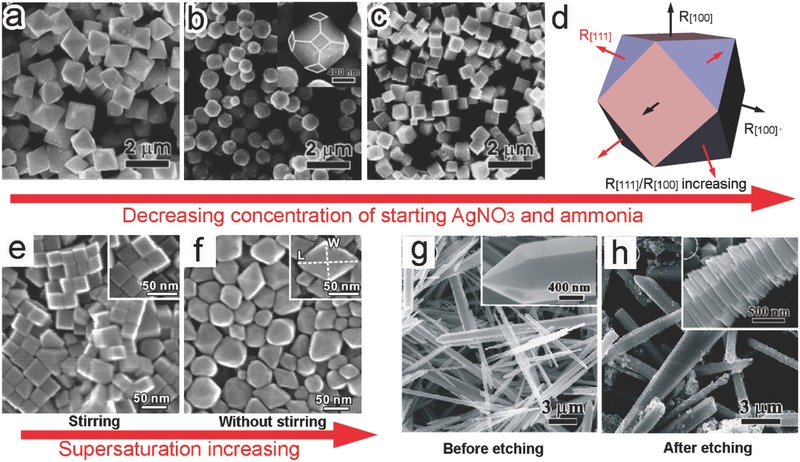
a–c) SEM images of Ag2O (a) octahedrons, (b) truncated octahedrons, and (c) cubes obtained through reducing the concentrations of starting materials. d) Schematic illustrating the corresponding synthetic mechanism. Reproduced with permission.35 Copyright 2010, American Chemical Society. e,f) SEM images of the (e) α‐Fe2O3 pseudocubes with {012} facets and (f) hexagonal bipyramidal α‐Fe2O3 with {113} facets prepared with and without solution stirring, respectively. Reproduced with permission.37 Copyright 2014, American Chemical Society. g,h) SEM images of ZnO columns (g) before and (h) after etching with OA. Reproduced with permission.40 Copyright 2010, American Chemical Society.
In addition to kinetic control, the facets of semiconductor crystals can be maneuvered in the thermodynamic regime. As a matter of fact, the use of facet‐selective capping agents falls into the category of thermodynamic control: the selective adsorption of capping agents to specific facets reduces their surface energies.34 Nevertheless, the capping agents are not indispensible for the thermodynamic control. From the viewpoint of thermodynamics, a polyhedron enclosed by a single facet is preferentially formed when the surface energy of this facet is sufficiently low as compared with others. As the surface energy difference between the facets is minimized, more than one facet will appear on the surface of crystals. According to the Thomson‐Gibbs equation, the surface energy of a facet is in proportion to the supersaturation during crystal growth,36 providing a knob for tuning surface facets. For instance, the exposed facets of α‐Fe2O3 nanocrystals could be simply tailored by controlling the supersaturation.37 Stirring reaction solution resulted in the formation of α‐Fe2O3 pseudocubes enclosed with {012} facets in the synthetic system that originally yielded hexagonal bipyramidal α‐Fe2O3 nanocrystals with {113} facets (Figure 4e,f). The formation of {113} facets with higher surface energy was achieved by increasing the supersaturation without stirring.
It should be noted that in most cases, the facet engineering for photocatalytic semiconductors involves both thermodynamic and kinetic control which take facet stability and relative growth rate into account.34, 38 These methods mainly manipuated the assembly of atoms into crystals and thus represent the bottom‐up approach to facet engineering. In sharp contrast, the directional chemical etching based on crystal anisotropy is a widely used top‐down approach to engineer the surface facets of semiconductor materials.23, 39 In a typical example, the facet evolution from ZnO hexagonal columns enclosed with nonpolar faces to pagoda‐like ZnO bounded by and polar planes has been achieved using oleic acid (OA) as a selective etching agent (Figure 4g,h).40 The reaction between Zn2+ cations and OA preferentially took place on the nonpolar faces composed of equivalent O2– and Zn2+ ions. In comparison, the etching rates were relatively lower on the O‐terminated and polar planes. During this process, the Zn2+ cations released from the etching would be nucleated and grown again to form hexagonal pyramids with stable polar facets.
3.2. Facet Control on the Surface of Multi‐Component Photocatalytic Materials
As photocatalytic materials are formed by combining multiple components, the facet adjustment for each component surface may benefit the optimization of photocatalytic performance as long as the surface participates in redox reactions. The complexity of hybrid structures increases the difficulty in simultaneously tailoring the exposed facets of components. Certainly this difficulty greatly depends on the combination methods for the components. The self‐assembly of two pre‐synthesized components offers the highest flexibility for facet engineering, as the facets of the components can be independently controlled in their own synthetic procedures.41 Another method is to in situ grow a new component on the surface of an existing one. In this synthetic system, the existing component serves as a seed and provides the growth sites in a seeding process. Similarly to the surface control of bare semiconductors, the facet of seeds can be facilely tailored by modifying the synthetic method.21, 42 However, it would be a challenge to maneuver the facet growth of the second component during the seeding process. In this section, the in situ synthetic approaches to surface facet control will be discussed according to architectural structures.
The supported structure is a widely used configuration for hybrid photocatalysts, in which the support is incompletely wetted by a newly formed component. To form this configuration, the exposed facet of new component is generally controlled by facet‐selective capping agents. For instance, capping agents have been employed to tailor the surface facets of TiO2 loaded on graphene nanosheets.43 To tailor the surface facets, different capping anions were used to guide the growth of crystalline TiO2 seeds into nanocrystals with graphene oxide and amorphous Ti(OH)4 as precursors (Figure 5 a).43 In the absence of capping agent, octahedral TiO2 nanocrystals enclosed by {101} facets (namely, TiO2‐101‐G) were formed. In comparison, TiO2 nanosheets dominated with {001} facets (TiO2‐001‐G) and TiO2 nanorods with {100} facets (TiO2‐100‐G) were formed on graphene when F− and SO4 2− were used as capping agents, respectively (Figure 5b–g). Certainly the use of capping agents is not limited to the surface facet adjustment for light‐harvesting semiconductors. The metal component in a hybrid structure is commonly controlled through a similar strategy. A typical case is to tailor the exposed facets of PdPt alloy nanocrystals that were supported on TiO2 nanosheets.44 In the synthesis, Br– and I– ions facilitated the in situ growth of Pd50Pt50 nanocubes enclosed with {100} planes on TiO2 nanosheets, while the synergistic use of HCHO and Na2C2O4 as capping agents resulted in the coverage of {111} planes on Pd50Pt50 nanotetrahedrons (Figure 5h–j).
Figure 5.
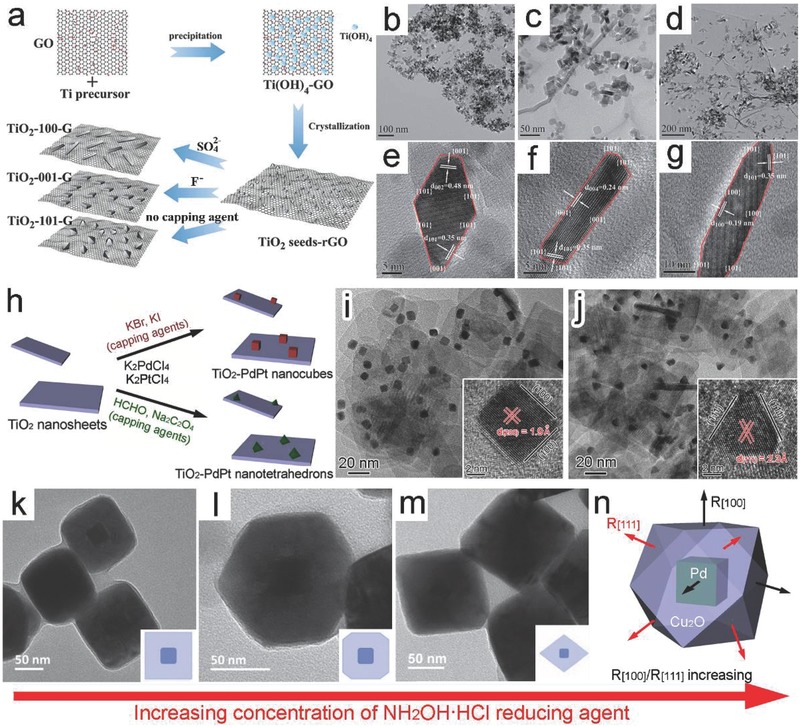
a) Schematic illustrating the synthesis of TiO2‐graphene nanocomposites with controllable TiO2 crystal facets. b–g) Transmission electron microscopy (TEM) and high‐resolution TEM (HRTEM) images of the as‐prepared (b,e) TiO2‐101‐G, (c,f) TiO2‐001‐G, and (d,g) TiO2‐100‐G. Reproduced with permission.43 h) Schematic illustration for the growth of PdPt cocatalysts enclosed with different facets on TiO2 nanosheets. i,j) TEM and HRTEM images of the as‐prepared (i) TiO2‐supported Pd50Pt50 nanocubes and (j) TiO2‐supported Pd50Pt50 nanotetrahedrons. Reproduced with permission.44 k–m) TEM images and scheme (inset) showing a gradual change in the shape of Cu2O shell from (k) cubes to (l) cuboctahedrons and then to (m) octahedrons in Pd‐Cu2O core‐shell structures through increasing the concentration of NH2OH·HCl. n) Schematic illustrating the corresponding synthetic mechanism. Reproduced with permission.46 Copyright 2013, Royal Society of Chemistry.
It is worth pointing out that controlling the exposed facet in a supported structure inevitably alters the interface facet between two components, as capping agents have their effects on the entire surface of the newly formed component. For instance, in the above TiO2‐PdPt hybrid structures, two different interfaces – TiO2{001}‐PdPt{100} and TiO2{001}‐PdPt{111} (Figure 5i,j) were formed when tailoring the surface facets of PdPt nanocrystals,44 which may induce distinct lattice mismatch at the interfaces. In contrast, the formation of core‐shell structures through an epitaxial growth offers an ideal platform for maintaining the quality of interfaces during the facet control. The exposed facet of the core can guide the epitaxial growth of shell component along crystal orientation to minimize the lattice mismatch. It has been revealed that the Au cores covered by {111} facets favor the formation of Au{111}‐Cu2O{111} interface, while the Au{100} facets provide growth sites for Au{100}‐Cu2O{100} interface.45 In the shell growth, thermodynamics or kinetics has to be tightly controlled for the rational facet adjustment. For instance, the exposed facets of Cu2O shells could be tailored by varying the amount of reducing agent during their epitaxial growth on Pd{100} cores.46 Increasing in the concentration of NH2OH·HCl, the shape of Cu2O gradually changed from cube to cuboctahedron and then to octahedron (Figure 5k–m). In other words, the exposed facets of Cu2O shells evolved from {100} to {111} while the Pd{100}‐Cu2O{100} interface was well maintained. This case perfectly highlights the importance of kinetic control: the growth rate of Cu2O in [111] direction (R[111]) is higher than that in [100] (R[100]) at low NH2OH·HCl concentration, and vice versa (Figure 5n).
3.3. Facet Control on the Interface of Multi‐Component Photocatalytic Materials
As claimed in Section 1, the interface of a hybrid structure largely determines the efficiency of photo‐induced charge carriers transferring through. Similarly to surface control, the difficulty for tailoring interfacial facets is dependent on the methods for integrating two components. During an epitaxial growth, the formation of a new component will minimize the lattice mismatch with the existing one toward the lowest interfacial energy,45, 47 reducing the flexibility of altering interfacial facets. Thus the interfacial facet adjustment is mainly accomplished in the supported structures through self‐assembly or non‐epitaxial growth. When both components are enclosed by or dominated with a single facet, the case is quite simple: the surface facets of two components determine the interfacial structure. However, when a component is covered by two or more facets, several different facet combination forms would be involved to complicate the case. In this section, we will mainly discuss how to control interfacial structures when a component is covered by multiple facets.
In the interface control, the use of facet‐selective capping agents is still a widely used method. The capping agents not only affect facet growth, but also preclude the deposition of a new component on the capped facets. This preclusion would selectively form an interface between the new component and the uncapped facets. For instance, Au nanoparticles were selectively deposited on the {100} planes of truncated octahedral Cu2O crystals using sodium dodecyl sulfate (SDS) as a capping agent.48 The preferential adsorption of SDS to Cu2O{111} effectively blocked the nucleation of Au on the {111} planes, and as such, a Cu2O{100}‐Au interface was rationally formed (Figure 6 a). Another similar case is the selective photodeposition of Au on ZnO nanorods.48 Au nanoparticles were formed on both top {0001} and side planes with Au(CH3COO)3 as a precursor (Figure 6b). As AuCl3 solution was used as an alternative Au3+ source, Cl– ions could be preferentially adsorbed on the polar {0001} planes to prevent the formation of ZnO{0001}‐Au interface (Figure 6c).
Figure 6.
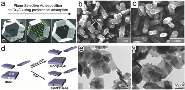
a) SEM images showing the facet‐selective Au deposition through the preferential adsorption of SDS to truncated octahedral Cu2O crystals. b,c) SEM images of the Au nanoparticles that were photochemically deposited on ZnO rods in (b) Au(CH3COO)3 and (c) AuCl3 ethanol solution, respectively. Reproduced with permission.48 Copyright 2009, American Chemical Society. d) Schematic illustration for the fabrication of different BiOCl‐Pd interfaces by employing PVP as a capping agent. e,f) TEM images of the obtained (e) BiOCl{001}‐Pd and (f) BiOCl{110}‐Pd hybrid structures. Reproduced with permission.22
In the use of capping agents, one may take advantage of component sizes and shapes. A typical example is the selective formation of BiOCl‐Pd interfaces on the BiOCl nanoplates with large {001} surface (Figure 6d).22 Due to the high {001} surface coverage, Pd nanocubes were predominately assembled on the top and bottom {001} surfaces of BiOCl nanoplates to form a BiOCl{001}‐Pd{100} interface (Figure 6e). When the BiOCl nanoplates were firstly treated with PVP, the adsorption of PVP to BiOCl{001} could preclude the loading of Pd nanocubes on the BiOCl{001} facet. As a result, Pd nanocubes were exclusively attached to the four side {110} faces to form a BiOCl{110}‐Pd{100} interface (Figure 6f).
Given the detrimental effect of residual polymeric capping agents on photocatalysis, facet‐dependent photodeposition has been developed as an alternative route to facet‐selective interface formation. The adjacent facets of a semiconductor crystal may possess different band structures so that the photogenerated electrons and holes are separately accumulated on the different facets (i.e., spatial charge separation). This feature provides a driving force to selectively deposit the new components on the facets through reduction or oxidation reactions.11, 20 For instance, a photodeposition method has been employed to load metal cocatalysts on the surface of single‐crystal decahedral Cu2WS4, in comparison with the conventional chemical deposition (Figure 7 a).49 The conduction band (CB) and valence band (VB) edges of Cu2WS4 {101} facet are 80 and 60 meV higher than those of {001} facet, respectively, accumulating photoexcited electrons on the {001} facet. During the photodeposition, the reduction of PtCl6 – mainly occurred on the {001} facets of Cu2WS4 to form a Cu2WS4{001}‐Pt interface (Figure 7b). In contrast, Pt nanoparticles were formed through reduction by ascorbic acid (AA) and randomly deposited on both {101} and {001} facets of Cu2WS4 in a photo‐free chemical deposition system (Figure 7c).
Figure 7.
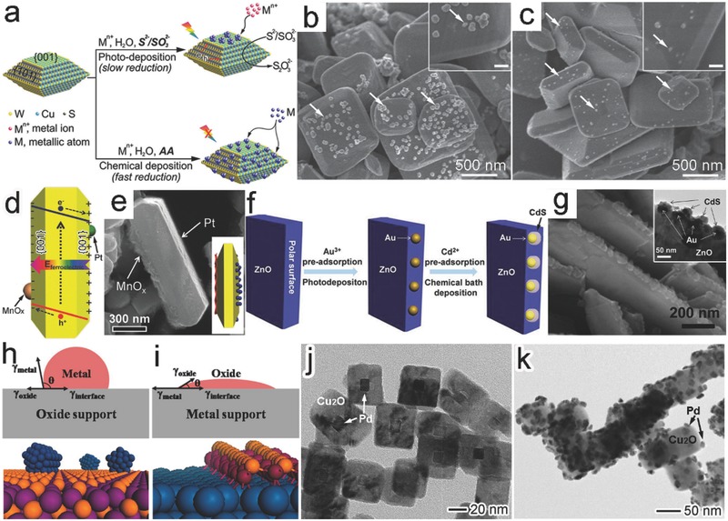
a) Schematic illustration for loading metal cocatalysts on a Cu2WS4 single crystal through photodeposition or chemical deposition. b,c) SEM images of 1 wt% Pt‐loaded Cu2WS4 photocatalysts prepared through (b) photoreduction and (c) chemical reduction, respectively. Reproduced with permission.49 d,e) Schematic illustration (d) and SEM image (e) for the selective deposition of MnOx and Pt at the two sides of {001} facet on PbTiO3 nanoplates. Reproduced with permission.52 Copyright 2014, Royal Society of Chemistry. f) Schematic illustration for the selective deposition of Au/CdS induced by the surface polar charges of ZnO. g) SEM and TEM (inset) images of the prepared CdS/Au/ZnO structure. Reproduced with permission.53 Copyright 2013, Royal Society of Chemistry. h,j) Schematics for the metal‐oxide interface in the (h) oxide‐supported metal structure and (j) oxide‐on‐metal inverse structure (γoxide is the surface energy of oxide, γmetal is the surface energy of metal, γinterface is the interface free energy, and θ is the contact angle). Reproduced with permission.57 Copyright 2013, American Chemical Society. j,k) TEM images of Cu2O‐Pd hybrid structures obtained with j) Pd nanocubes and k) Cu2O nanocubes as existing components, respectively. Reproduced with permission.58
The internal electric field built in ferroelectric materials or between polar facets can play a similar role in selective accumulation of electrons or holes. The field promotes the electron‐hole separation along a particular direction and accumulates electrons and holes on the two side facets perpendicular to the field direction.11, 50, 51 This charge accumulation provides the opportunity for selecting facets to form interfaces through photo‐deposition. For instance, an internal electric field is built in ferroelectric PbTiO3 nanoplates along the [001] direction, so the photogenerated electrons and holes diffuse to the positively and negatively charged {001} facets, respectively (Figure 7d).52 As such, when H2PtCl6 and MnSO4 were simultaneously photochemically reduced and oxidized, Pt and MnOx would be asymmetrically deposited on the positively and negatively charged {001} facets of PbTiO3, respectively, forming two difference interfaces (Figure 7e).
The polar facets, which are enriched with opposite surface charges owing to their different termination patterns of bonding networks,11 may provide an alternative approach to the facet‐dependent photodeposition for interface design. Due to electrostatic interaction, the reactant anions or cations for component deposition are attracted to the positively or negatively charged facets, respectively, offering the facet‐dependent selective deposition. For instance, Au nanoparticles could be selectively deposited on the lateral plane of ZnO nanosheets, in which the Au‐based complex ions were attached to the negatively charged O‐terminated facet and then photo‐reduced into Au nanoparticles (Figure 7f).53 Further with the Cd‐based complex ions, CdS was coated around the Au nanoparticles on the O‐ polar surface to form a CdS/Au/ZnO heterostructure (Figure 7f,g). Similarly the facet‐selective deposition of Pt on platelike WO3 was achieved through the dark sorption of [PtCl6]2– on positively charged {020} facets. The efficiency of this selective deposition has been proven dependent on the pH value – a key parameter to electrostatic interaction.54
In terms of facet‐selective interface formation,45, 55, 56 the interfacial wetting of components is an important factor that has to be taken into account. For instance, as metals have larger surface energy than oxides, the metals can hardly wet the surface oxides according to Young's equation. On the contrary, wetting metal surface with oxides can be more readily achieved. For this reason, the surface facets of metals provide stronger guidance for the formation of interface with oxides (Figure 7h,i).57 For instance, in the synthesis of Cu2O‐Pd hybrid structures, the interface formation underwent different situations when Pd nanocubes and Cu2O nanocubes were used as starting components, respectively.58 The {100} planes of Pd nanocubes directed the formation of Pd{100}‐Cu2O{100} interface; however, the same interface could not be formed when the Cu2O nanocubes enclosed with {100} facet were used as the starting material (Figure 7j,k).
4. Facet Engineering for Mono‐Component Photocatalytic Materials
4.1. Large Percentage of Surface Facets with High Photocatalytic Activity
Section 3 has elucidated the synthetic approaches to engineering the facets at the surface and interface of photocatalytic materials. We are now in a position to discuss the design of high‐performance photocatalysts based on facet engineering. In the surface design of mono‐component semiconductor materials, the simplest way is to increase the percentage of the exposed facets with higher photocatalytic activity and selectivity. The large coverage of one facet on surface would facilitate the investigations on facet‐dependent photocatalytic performance and related mechanisms. Furthermore, the understanding gained from the mechanism research can provide a guidance for identifying the high‐activity facet for enhanced photocatalytic performance. This two‐way research mode has been widely used for the development of facet‐engineered photocatalysts.
The exposed facets may impact on photocatalytic performance through multiple effects. The most direct effect from surface facets is associated with the dangling bonds and low‐coordinated atoms at terraces, steps, kinks, adatoms, and vacancies. In addition to their different surface energies, these structural features affect the adsorption and activation of reactant molecules, varying photocatalytic activity and selectivity.59 For instance, anatase TiO2 nanooctahedrons (Figure 8 a), nanobelts (Figure 8b), and nanoplates (Figure 8c) were dominated with or enclosed by {101}, {010} and {001} facets, respectively. Their performance comparison revealed that {001}‐TiO2 provided 1.79 and 3.22 times higher reaction rates than {010}‐ and {101}‐TiO2 in photocatalytic degradation of methyl orange (MO), respectively (Figure 8d),60 as the {001} facet possessed higher surface energy and a larger number of coordinatively unsaturated Ti4+ active sites. In another case, the Ag3PO4 rhombic dodecahedrons enclosed by twelve {110} facets (Figure 8e) exhibited superior photocatalytic activity to the cubes bounded by six {100} facets (Figure 8f) in degradation of MO (Figure 8g) and rhodamine B (RhB) (Figure 8h).61 The density functional theory (DFT) calculation revealed that the surface energy of {110} facets (1.31 J/m2) was higher than that of {100} facets (1.12 J/m2), indicating the higher reactivity of {110} facets.
Figure 8.
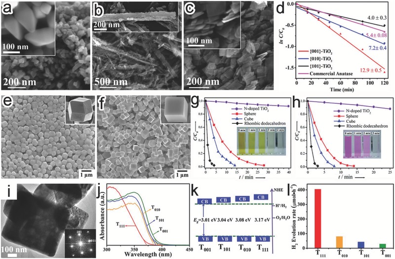
a–c) SEM images of (a) {101}‐TiO2, (b) {010}‐TiO2, and (c) {001}‐TiO2. d) pseudo‐first‐order plots for MO photodegradation using the differently faceted TiO2. Reproduced with permission.60 Copyright 2015, American Chemical Society. e–h) SEM images of Ag3PO4 (e) rhombic dodecahedrons and (f) cubes as well as their photocatalytic activities in (g) MO and (h) RhB degradation under visible‐light irradiation. Reproduced with permission.61 Copyright 2011, American Chemical Society. i) TEM image of TiO2 with {111} surface facets. j) UV‐visible absorption spectra of the TiO2 samples. k) Schematic illustration for the determined VB and CB edges of the TiO2 samples. l) Photocatalytic water splitting performance by Pt‐loaded (0.5%) TiO2 samples. Reproduced with permission.17 Copyright 2013, American Chemical Society.
From the viewpoint of charge kinetics, the surface facets of semiconductors may possess different electronic band structures, caused by their atomic arrangements. The shift of CB and VB energy levels by surface states would directly alter the reduction and oxidation potentials of photogenerated carriers, respectively.11, 32 This feature has been recognized in the photocatalytic activity comparison between square‐shaped TiO2 plate covered by {111} facet (T111, Figure 8i) and TiO2 mainly enclosed with {001}, {101} or {010} facets (named as T001, T101 or T010).17 Ultraviolet (UV)‐visible absorption spectroscopy revealed that the bandgaps of T001, T101, T010 and T111 were 3.01, 3.04, 3.08 and 3.17 eV, respectively (Figure 8j). Despite their comparable VB maxima (VBMs), the four samples have CB minima (CBMs) in the order of T111 > T010 > T101 > T001 (Figure 8k). As a higher CBM can offer the electrons with higher potential for photocatalytic reduction reaction, the photocatalytic H2 evolution rate by the samples followed the same order as CBMs (T111 > T010 > T101 > T001) (Figure 8l).
Another important effect from surface facets is the dependence of charge transfer and separation on crystal orientation from two angles, intrinsically driven by internal electric field. Firstly, polar facets may spontaneously induce a polarization effect.11, 50 In the CoO octahedrons enclosed with polar {111} plane (Figure 9 a), internal electric field was established through the spontaneous polarization between the alternate layers of positive Co2+ ions and negative O2– ions along the [111] direction (Figure 9b).62 The electric field could drive the migration of photogenerated electrons toward the positive polar Co‐CoO{111}, , and surfaces for reduction reaction, along with the hole transfer to negative polar O‐CoO, , and for oxidation reaction (Figure 9c). Secondly, a spontaneous polarization takes place in ferroelectric materials as their positive and negative charges have different centers of symmetry.11, 50, 51 For instance, ferroelectric Bi4Ti3O12 nanosheets were dominant with {001} facets (Figure 9d),63 and exhibited a spontaneous polarization of 4 μC cm–2 along the c‐axis. The internal electric field drove the separation of the photogenerated electrons and holes and their diffusion along [001] direction (Figure 9e). The electrons and holes would be eventually accumulated on the two sides of the {001} facet, resulting in the superb photocatalytic activity of this facet.
Figure 9.
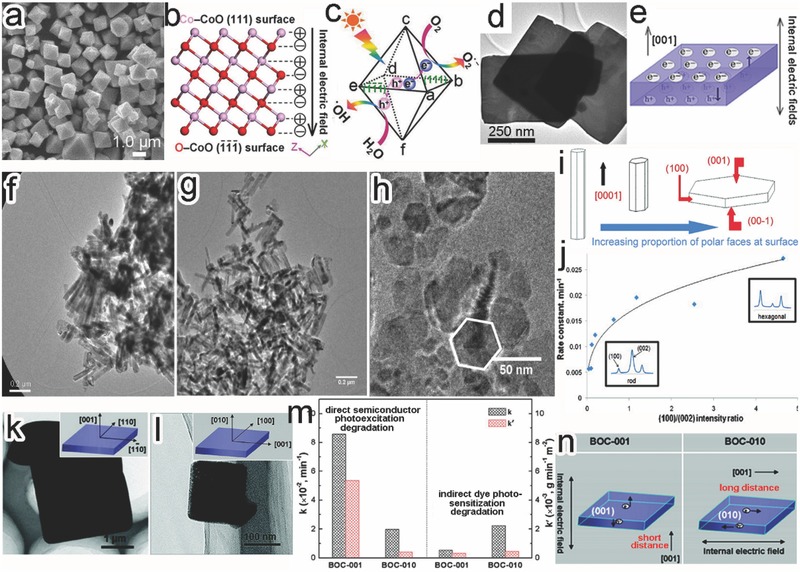
a) SEM image of CoO octahedrons. b) Atomic charge distribution of CoO {111} and facets. c) Schematic illustration for the charge separation between polar {111} surfaces. Reproduced with permission.62 Copyright 2015, American Chemical Society. d) TEM image of Bi4Ti3O12 nanosheets dominated with {001} facets. e) Schematic illustration for the charge separation along [110] direction. Reproduced with permission.63 Copyright 2014, Elsevier. f–h) TEM images of (f) long ZnO rods, (g) short ZnO rods, and (h) hexagonal ZnO plates. i) Schematic diagrams showing the increased proportion of polar facets from rods to plates. j) Plot of the rate constants vs. (100)/(002) intensity ratio in MB photodegradation. Reproduced with permission.64 Copyright 2009, American Chemical Society. k,l) TEM images and scheme (inset) of (k) BOC‐001 and (l) BOC‐010. m) Comparison of reaction rate constants between BOC‐001 and BOC‐010 in MO degradation under (left) UV and (right) visible‐light irradiation. n) Schematic for the corresponding mechanism. Reproduced with permission.18 Copyright 2012, American Chemical Society.
In a similar case, the ZnO long nanorods, short nanorods and hexagonal plates, with the increased proportion of {001} polar faces, were used as photocatalysts in degradation of methylene blue (MB) (Figure 9f–i).64 The reaction rates turned out to promote with the increase of {001} proportion, suggesting that the terminal polar {001} and facets were more active in the reaction (Figure 9j). Certainly the shape evolution from ZnO nanorods to nanoplates reduced the distance along the [001] direction for charge transfer and separation as well, contributing to the performance enhancement. Similarly, the BiOCl nanosheets enclosed with {001} facets (BOC‐001) showed higher photocatalytic activity in both the direct semiconductor photoexcitation degradation and indirect dye photosensitization degradation of MO, as compared with BiOCl nanosheets dominated with {010} facets (BOC‐010) (Figure 9k‐m).18 In this system, an internal electric field assisted the charge separation and transfer along the [001] direction in the BiOCl crystal structures, designating the direction of charge kinetics. As such, the BOC‐001 became more favorable in charge separation and transfer as its smaller dimension in the [001] direction substantially shortened the diffusion distance of photoinduced charge carriers (Figure 9n).
Overall, increasing the percentage of high activity facets is a versatile approach to develop highly efficient photocatalysts, which calls for the fundamental research on facet‐dependent performance assessement and mechanism investigation. In general, two major schemes have widely used in the pursuit of covering a semiconductor with a large portion of highly reactive facets. One is to develop symmetric polyhedral micro/nanocrystals enclosed by the high‐activity facet, such as the aforementioned Ag3PO4 rhombic dodecahedron enclosed by {110} facet (Figure 8e) and CoO octahedron enclosed by polar {111} facet (Figure 9a).61, 62 However, symmetric polyhedral structures have been rarely reported for few semiconductors which mainly possess a body‐centered cubic or face‐centered cubic crystal structure. Thus the other scheme that two‐dimensional micro/nanostructures have high‐activity facets on their flat surfaces has been more extensively explored in recent years. The typical examples include the TiO2 nanosheets with top and bottom planes of {001} facets (Figure 8c), TiO2 plates with majority {111} facets (Figure 8i), and Bi4Ti3O12 nanosheets (Figure 9d) and ZnO nanoplates (Figure 9h) dominated with polar {001} facets.17, 60, 63, 64
Table 1 summarizes the facet‐dependent activities of semiconductors in various photocatalytic reactions and the corresponding mechanisms, together with the photocatalyst shapes with high activity. It clearly shows that the activity of a facet is strongly dependent on the type of photocatalytic reactions and the related catalytic mechanisms. For example, the activity of anatase TiO2 facets in degradation of dyes are in the order: {001}>{010}>{101},60 while a different order ({010}>{101}>{001}) has been resolved for photocatalytic H2 evolution.17, 32 This feature manifests that the species adsorption and activation plays a more prominent role in dye degradation, while the water splitting raises higher demand for band structures.85 In many cases, the activity of a facet is influenced by a mix of different catalytic mechanisms. For instance, both internal electronic field and species adsorption contributed to the superior photocatalytic activity of BiOBr{001} to BiOBr{010} in degradation of 2,4‐dichlorophenol and inactivation of Escherichia coli;74, 75 CeO2{100} and CeO2{110} offered suitable band structure for generating more energetic holes and more O vacancies for catalytic active sites, respectively, which caused to exhibit different photoreactivitiy in photocatalytic oxidation of volatile organic compound and O2 evolution reaction.79
Table 1.
Facet‐dependent activity of semiconductors in various photocatalytic reactions as well as their corresponding mechanisms
| Semiconductor | Crystal phase | Facet activity comparison | Photocatalytic reaction | Mechanism | Shape of semiconductor (dominated/enclosed with high activity facet) | Ref. |
|---|---|---|---|---|---|---|
| TiO2 | Anatase | {001}>{010}>{101} | Degradation of MO | Adsorption and activation | Sheet (Dominated) | 60 |
| Ag3PO4 | Body‐centered cubic | {110}>{100} | Degradation of MO and RhB | Adsorption and activation | Rhombic dodecahedron (Enclosed) | 61 |
| TiO2 | Anatase | {111}>{010}>{101}>{001} | H2 evolution from water | Band structures/adsorption and activation | Plate (Dominated) | 17 |
| ZnO | Hexagonal wurtzite | {001}>{100} | Degradation of MB | Direction of charge transfer and separation | Hexagonal plate (Dominated) | 64 |
| BiOCl | Tetragonal | {001}>{010} | Degradation of MO | Direction of charge transfer and separation | Plate (Dominated) | 18 |
| Cu2O | Face‐centered cubic | {111}>{100} | Degradation of MO | Adsorption and activation | Octahedron (Enclosed) | 29, 65 |
| TiO2 | Anatase | {010}>{101}>{001} | Hydroxyl radicals production\H2 evolution from water | Band structures/adsorption and activation | Cuboid (Dominated) | 32, 66 |
| TiO2 | Anatase | {010}>{101}>{001} | Reduction of CO2 | Adsorption and activation | Rod (Dominated) | 67 |
| Cu2O | Face‐centered cubic | {110}>{100} | Degradation of MO | Adsorption and activation | Rhombic dodecahedra (Enclosed) | 68 |
| AgBr | Face‐centered cubic | {111}>{100} | Degradation of MO | Adsorption and activation | Octahedron (Enclosed) | 69 |
| Ag2O | Face‐centered cubic | {100}>{110}>{111} | Degradation of MO | Adsorption and activation | Cube (Enclosed) | 70, 71 |
| BiOI | Tetragonal | {110}>{001} | Degradation of bisphenol | Adsorption and activation/band structures | Sheet (Dominated) | 72 |
| Ag3PO4 | Body‐centered cubic | {111}>{100}>{110} | O2 evolution from water | Adsorption and activation/direction of charge transfer and separation | Tetrahedron (Enclosed) | 73 |
| BiOBr | Tetragonal | {001}>{010} | Degradation of 2,4‐dichlorophenol | Adsorption and activation/direction of charge transfer and separation | Sheet (Dominated) | 74 |
| Inactivation of Escherichia coli | 75 | |||||
| CdS | Hexagonal | {0001}> | H2 evolution from water | Adsorption and activation/band structures | Plate (Dominated) | 76 |
| Ag2WO4 | Orthorhombic | {110}>{011}>{010}> | Degradation of RhB and Rhodamine 6G (Rh6G) dyes | Adsorption and activation | Hexagonal rod (Dominated) | 77 |
| BiOCl | Tetragonal | {010}>{001} | Degradation of 2‐naphthol | Adsorption and activation | Sheet (Dominated) | 78 |
| CeO2 | Cubic fluorite | {100}>{110} | Oxidation of volatile organic compounds | Band structures | Cube (Enclosed) | 79 |
| {110}>{100} | O2 evolution from water | Adsorption and activation | Rod (Dominated) | |||
| SrTiO3 | Cubic | {101}>{100} | Degradation of RhB and MO | Adsorption and activation | Triangular prisms (Dominated) | 80 |
| SrTiO3 | Cubic | {100}>{110} | Decomposition of acetic acid | Direction of charge transfer and separation | Cube (Enclosed) | 81 |
| {110}>{100} | H2 evolution from water | Flake (Dominated) | ||||
| AgCl | Face‐centered cubic | {100}>{111} | Degradation of MO and RhB | Band structures | Cube (Enclosed) | 82 |
| AgCl | Face‐centered cubic | {15 5 2}>{311}>{111} | Degradation of MO | Adsorption and activation | Concave hexoctahedron (Enclosed) | 83 |
| BiOBr | Tetragonal | {102}>{001} | Degradation of RhB | Band structures | Sheet (Dominated) | 84 |
4.2. Synergism between Different Surface Facets with Optimal Ratios
According to the analysis above, it is anticipated that a high proportion of high‐activity facet on surface would promote the performance of photocatalytic materials. However, in some cases, a synergism of different facets on the surface of semiconductor crystals may also further enhance their photocatalytic activity. As discussed above, the electrons and holes are separately accumulated on the different facets of a semiconductor, driven by their different band structures, thereby reducing the adverse electron‐hole recombination. Moreover, spatially separating reduction from oxidiation sites by different facets may also prevent the back reaction between reduction and oxidation products. The work by Liu et al. provided a very straightforward proof for the synergism of different facets in achieving the enhanced photocatalytic activity.86 They compared the photocatalytic H2 production by a group of anatase TiO2 nanocrystals with tunable percentages of {001} facet area from 0 to 51.2% (Figure 10 a–e). The truncated tetragonal bipyramidal TiO2 sample with 14.9% {001} facets turned out to achieve the highest photocatalytic activity, well exceeding those by the octahedral TiO2 fully enclosed by {101} facets or the sample with highest {001} percentage (51.2%) (Figure 10f). In the case of mixed {101} and {001} facets, the photogenerated electrons and holes migrated toward {101} and {001} facets, respectively, balancing their recombination and reaction rates.
Figure 10.
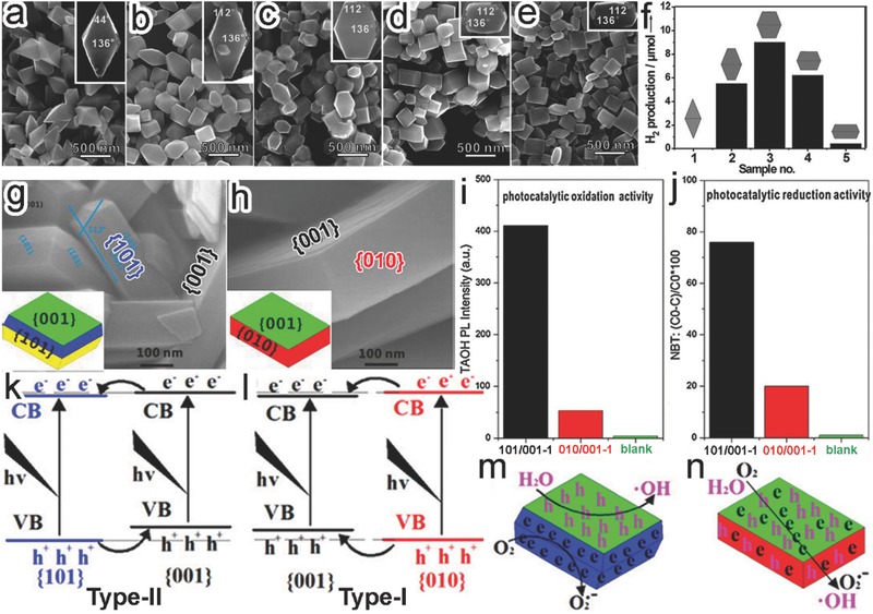
a–e) SEM images of TiO2 nanocrystals with the increased ratios of exposed {001} to {101} facets. f) Photocatalytic hydrogen production by the TiO2 with different exposed facets. Reproduced with permission.86 g,h) SEM images and scheme (inset) of (g) {101}/{001} and (h) {010}/{001} TiO2 samples. i,j) Comparison of photocatalytic (i) oxidation and (j) reduction activity by the {101}/{001} and {010}/{001} samples. k–n) Electronic band structures and charge distribution of the (k,m) type‐II {101}/{001} and (l,n) type‐I {010}/{001} samples. Reproduced with permission.87 Copyright 2013, Elsevier.
It should be noted that only when the electronic structures of two facets are satisfied with the Type‐II (staggered) band alignment (i.e., one facet has higher CBM and VBM than the other one), can the spatial charge separation be achieved. In a typical case, anatase TiO2 crystals with {101}/{001} (Figure 10g) and {010}/{001} (Figure 10h) coexistence facets were synthesized by Ye et al., respectively.87 The {101}/{001} TiO2 possessed significantly higher photocatalytic activity than {010}/{001} TiO2 in both oxidation and reduction reactions (Figure 10i,j) owing to their unique Type‐II band alignment. Both the CBM and VBM of {001} facet were higher than those of {101} in the {101}/{001} TiO2, forming a Type‐II band alignment. As such, the photoinduced electrons and holes would transfer to {101} and {001} facets, respectively, which accomplished the spatial charge separation between the two facets (Figure 10k). When {101} facets were replaced by {010}, a Type‐I (straddling) band alignment would be formed as the CBM and VBM of {010} facets were higher and lower than those of {001}, respectively. In this case, most electrons and holes would transfer to the {001} facets together and would be no longer separated (Figure 10l). As a result, the photocatalytic reduction and oxidation by {101}/{001} TiO2 should take place on {001} and {101} facets, respectively, whereas the two half reactions could not be spatially separated in {010}/{001} TiO2 (Figure 10 m,n). As summaried in Table 2 , thus far the spatial charge separation between different facets has been validated for various semiconductor micro/nanocrystals covered by two or more facets.
Table 2.
Spatial charge separation between different facets in various photocatalytic semiconductors
| Semiconductor | Crystal phase | Shape of semiconductor | Facet for reduction reaction | Facet for oxidation reaction | Ref. |
|---|---|---|---|---|---|
| TiO2 | Anatase | Tetragonal bipyramid | {101} | {001} | 86, 87, 88, 89, 90, 91, 92 |
| BiVO4 | Monoclinic | Tetragonal bipyramid | {010} | {110} | 20, 93, 94, 95 |
| BiOCl | Tetragonal | Sheet | {001} | {110} | 22, 96 |
| CeO2 | Body‐centered cubic | Hexahedron prism‐anchored octahedron | {111} | {100} | 97 |
| Cu2O | Face‐centered cubic | Cuboctahedron | {100} | {111} | 21 |
| Cu2WS4 | Decahedral | Tetragonal bipyramid | {001} | {101} | 49, 98 |
| TiO2 | Brookite | Sheet | {210}/{101} | {201} | 99 |
| TiO2 | Rutile | Tetragonal prism | {110} | {011} | 100 |
| TiO2 | Anatase | Cuboid | {101} | {001}/{100} | 101 |
| TiO2 | Anatase | Truncated tetragonal bipyramid | {101} | {001}/{110} | 102 |
| SrTiO3 | Cubic | Tetrahexahedron | {001} | {023} | 103, 104 |
| BaLa4Ti4O15 | Perovskite | Sheet | {111} | {110} | 105, 106 |
| Cu2O | Face‐centered cubic | 26‐facet polyhedral cube | {100} | {111} | 107 |
| Cu2O | Face‐centered cubic | Concave cubooctahedron | {104} | {100} | 108 |
To maximize the synergistic effect between different semiconductor facets, one can optimize the exposed area ratio of the synergism facets. For instance, the photocatalytic CO2 reduction activity by anatase TiO2 was enhanced by exposing both {001} and {101} facets on TiO2 surface.88 Adjusting the amounts of HF, the ratio of the exposed TiO2 {101} to {001} facets could be tuned from 89:11 (i.e., {101}‐dominated octahedral bipyramid, HF0) to 17:83 (i.e., {001}‐dominated nanoplates, HF9) (Figure 11 a–c). With photocatalytic CO2 reduction as a model reaction, it revealed that the optimal facet ratio was 45:55 (i.e., HF4.5) for achieving the highest CH4 production (Figure 11d). As a Type II band alignment was formed between {101} and {001} facets, photogenerated electrons and holes would migrate toward {101} and {001} facets, respectively, during the photocatalytic process (Figure 11e). As illustrated in Figure 11f, most of the photogenerated electrons and holes in the HF0 were mainly accumulated on the {101} facets due to the low percentages of {001} facet, inducing serious charge carrier recombination. The similar situation happend for the HF9 in which the charge carriers were accumulated and recombined on the {001} facet. Only in the optimal ratio of {101} to {001} facets (i.e., 45:55, HF4.5), the most efficient spatial charge separation could be achieved for reduction and oxidation reactions.
Figure 11.
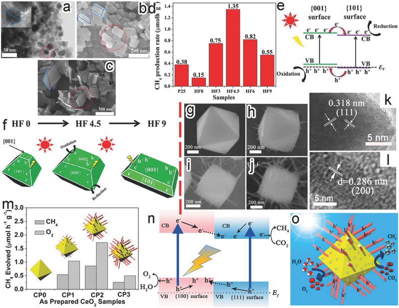
a–c) TEM and SEM images of TiO2 nanocrystals with the increased ratios of exposed {001} to {101} by varying HF amount: (a) HF0, (b) HF4.5, and (c) HF9. d) Photocatalytic CH4 production activity by the TiO2 samples. e) Electronic band structures for {001} and {101} facets. f) Schematic illustration for the spatial separation on the HF0, HF4.5, and HF9 samples designating redox sites. Reproduced with permission.88 Copyright 2014, American Chemical Society. g–j) SEM images of (g) CeO2 octahedrons and (h–j) hexahedron prism‐anchored CeO2 octahedrons with the increased portions of hexahedron prisms. k,l) HRTEM images for the (k) octahedron and (l) prism in the hexahedron prism‐anchored octahedronal CeO2, respectively. m) CH4 and O2 generation rates by the samples of redox sites with 0.5% wt Pt. n,o) Schematic illustration for (n) the spatial charge separation between {001} and {111} facet and (o) the photocatalytic mechanism of the CeO2 homojunction. Reproduced with permission.97 Copyright 2015, American Chemical Society.
As limited by the crystal structures and synthetic techniques, not all the combinations of two facets can be achieved in a single‐domain crystal. Thus the artificial synthesis of crystal facet‐based homojunctions offers an alternative approach to achieve the synergism between two facets through spatial charge separation. An excellent demonstration is the CeO2 homojunction consisting of hexahedron prism‐anchored octahedron fabricated through crystallographic‐oriented epitaxial growth.97 The hexahedron prism‐anchored CeO2 octahedrons and bare CeO2 octahedrons were selectively obtained by controlling the addition of phosphate ions (Figure 11g,h). Increasing the concentrations of phosphate ions, the prism arms became denser, longer and thicker (Figure 11h–j). As shown in HRTEM images, the CeO2 octahedrons and hexahedron prisms were enclosed with {111} and {100} facets, respectively (Figure 11k,l). When the samples were used in photocatalytic reduction of CO2, no hydrocarbon species product was found for bare CeO2 octahedrons while hexahedron prism‐anchored octahedrons exhibited distinct photocatalytic activity in CH4 generation (Figure 11m). With the increase of hexahedron prism arms, the CH4 generation rates displayed a volcano trend, suggesting the synergistic effect between {111} and {100} facets. An optimal {111}/{100} ratio ensured to obtain the highest photocatalytic activity. Figure 11n shows the Type II band alignment between {111} and {100} facets, in which the photogenerated electrons and holes transferred to the CB of {111} and the VB of {100} facets, respectively. Driven by this spatial charge separation, the electrons were accumulated on {111} facets to perform the reduction of CO2 to CH4, and the holes were gathered on {100} facets for H2O oxidation (Figure 11o).
5. Facet Engineering for Multi‐Component Photocatalytic Materials
5.1. Facet‐Engineered Surface Design
In a multi‐component hybrid structure, junctions are mainly formed through the combination of a semiconductor with other materials (e.g., semiconductors, metals, and carbon materials) to form different charge kinetic models.11, 14, 109 To promote the performance of a component participating in surface catalytic reactions, the surface facet of this component should be tightly controlled. Meanwhile, the facet adjustment would inevitably result in variations in its interfacial structure with other components in contact. This factor should certainly be considered; otherwise, interfacial charge transfer would become the bottleneck of the entire charge kinetics in photocatalysis so as to reduce the efficacy of surface design.
A hybrid structure involves multiple components including the light‐harvesting semiconductor and other materials, all for which the surface facet design can be performed. The case of semiconductor component is relatively straightforward: the designing rules in Section 4 can be directly implemented. For instance, the graphene‐supported TiO2 nanosheets dominated with {001} facet have been widely used as photocatalysts for dye degradation mainly owing to the high activity of TiO2{001} facet;110, 111, 112 the Ag3PO4 tetrahedrons were integrated with C3N4 nanosheets for photocatalytic MB degradation by taking advantage of the highest activity of Ag3PO4{111} facet.113
Nevertheless, we have to point out that the selection of a high‐activity semiconductor facet does not necessarily guarantee the high photocatalytic activity of semiconductor‐based hybrid structure. As mentioned in Section 4, the UV‐excitable BiOCl nanosheets dominated with {001} facets (BOC‐001) possessed higher photocatalytic activity than BOC‐010, owing to the internal electric field along [001] direction.18 However, the situation totally changed when the g‐C3N4 nanoparticles – a visible‐light semiconductor sensitizer – were loaded on BOC‐001 and BOC‐010 nanosheets. The ng‐CN/BOC‐010 heterojunction photocatalysts exhibited superior photocatalytic performance to ng‐CN/BOC‐001 in MO degradation under visible‐light irradiation (Figure 12 a). Although the photogenerated electrons could effectively migrate from the CB of n‐C3N4 to the CB of BiOCl in both composites (Figure 12b), driven by the [001]‐orientated internal electric field in BiOCl, the traveling lengths for electron transfer were quite different. The electrons in ng‐CN/BOC‐001 were required to travel within the BOC‐001 bulk, while the electron transfer in ng‐CN/BOC‐010 occurred along the BOC‐010 surface. Apparently, the BOC‐010 offered a shorter distance for charge transport, lowering the loss of electrons during their delivery to reduction reaction sites (Figure 12c).114
Figure 12.
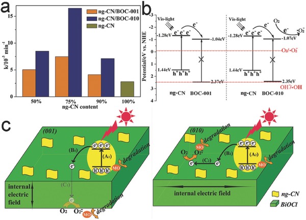
a) Visible‐light‐induced photocatalytic degradation of MO over bare ng‐CN, ng‐CN/BOC‐001 and ng‐CN/BOC‐010 heterojunction photocatalysts containing different proportions of ng‐CN. b) Band alignments in ng‐CN/BOC‐001 and ng‐CN/BOC‐010 heterojunction photocatalysts. c) Proposed mechanism for photocatalytic reactions occurring on ng‐CN/BOC‐001 and ng‐CN/BOC‐010 heterojunction photocatalysts. Reproduced with permission.114 Copyright 2015, Royal Society of Chemistry.
Similarly, Pt loading can alter the activity order of anatase TiO2{001} and {010} facets for the photocatalytic reduction of CO2 to CH4.115 In the absence of Pt loading, TiO2{010} facet exhibited higher activity in photocatalytic CO2 reduction in comparison with TiO2{001}, attributing to the stronger CO2 adsorption and longer charge lifetime of TiO2{010}. Further integrated with small Pt nanoparticles, however, the TiO2{001} sample offered more efficient electron‐hole separation than the Pt‐TiO2{010} junction, enabling higher photocatalytic activity. This case further emphasizes that the significant impact of interface on charge transfer should not be neglected when the surface facets of photocatalytic hybrid structures are tailored.
In terms of Pt loading, the cocatalysts – Pt nanoparticles – not only trap the electrons to promote charge separation, but also provide active sites for CO2 adsorption and activation. As such, photocatalytic performance is no longer dependent on the activity of TiO2 facets.115, 116 Given the role of cocatalysts as reactant adsorption and activation sites, it would be straightforward to tune the photocatalytic performance by tailoring the surface facets of cocatalysts while maintaining the exposed facet of light‐harvesting semiconductor.117 In a typical case, we have tuned the selectivity of C3N4‐Pd hybrid structures in photocatalytic CO2 reduction in present of H2O through adjusting the surface facets of Pd cocatalysts.118 When the {100}‐faceted Pd nanocubes were supported on the g‐C3N4 nanosheets, the photocatalyst preferred to undergo the reduction of H2O to H2. In contrast, with the Pd nanotetrahedrons enclosed with {111} facets as cocatalyst, photocatalytic reduction mainly took place along the reduction of CO2 to carbon products (e.g., CO, C2H5OH, and CH4) (Figure 13 a,b). The selectivity for CO2 reduction was 20.7% of C3N4‐Pd nanocubes versus 78.1% of C3N4‐Pd nanotetrahedrons (Figure 13c), simply because the Pd{111} and Pd{100} facets offered higher adsorption and activation abilities for CO2 and H2O, respectively (Figure 13d). It should be pointed out that ensuring the equivalent efficiency of interfacial charge transfer is a prerequisite for reliably assessing the facet‐dependent reaction selectivity. In the case of g‐C3N4, this prerequisite was ensured by the unique conjugated structure of C3N4 which offered multiple coupling configurations with Pd facets in C3N4‐Pd{100} and C3N4‐Pd{111}. In addition to Pd, the surface facets of Pt and PdPt alloy cocatalysts have been reported to play an important role in the surface H2O adsorption and activation for photocatalytic H2 evolution.44, 119
Figure 13.
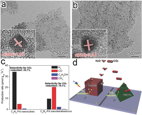
a,b) TEM and HRTEM (inset) images of (a) C3N4‐Pd nanocubes enclosed with Pd{100} facets and (b) C3N4‐Pd nanotetrahedrons with Pd{111} facets. c) Photocatalytic generation rates of H2 and carbon products by the catalysts with ca. 6 wt% Pd loading. d) Schematic illustration for the photocatalytic CO2 reduction in presence of H2O on C3N4‐Pd hybrid structures. Reproduced with permission.118 Copyright 2014, Royal Society of Chemistry.
5.2. Facet‐Engineered Interface Design
As briefly mentioned above, facet‐engineered interface design is a highly important theme to photocatalytic hybrid materials. As the interface is formed by integrating two components in contact, the design of interfacial facets can be carried out through tailoring the exposed facet of either semiconductor or other components (or a second semiconductor).43, 120 However, the variation in the component surface facets may also alter the process of surface reactions, complicating the correlation of photocatalytic performance with interfacial facets. As discussed in Section 3.3, it is a more straightforward strategy for simplifying the case by selectively depositing a new component on the different facets of an existing one.20, 49 On the whole, the main mission for facet‐engineered interface design is to select suitable component facets for forming the interface toward efficient charge transfer.
In general, there are multiple factors affecting interfacial charge transfer efficiency. The first factor is the ability of accepting photogenerated electrons or holes correlated with the facets of semiconductor. This correlation is caused by the spatial charge separation between adjacent facets or the internal electronic field along a particular crystal orientation as discussed above. For this reason, a suitable facet of semiconductor should be selected for the formation of interface with cocatalysts. As the cocatalysts trap electrons (or holes) and provide reactive sites for reduction (or oxidation) reactions, the selective deposition of reduction (or oxidation) cocatalysts on the electron (or hole)‐accumulated facets should be favorable to the overall photocatalytic performance. By rationally engineering the interfacial facets, the role of cocatalysts in charge trapping further promotes the spatial charge separation between different facets and prevents the back reactions of products. Furthermore, the accumulation of charge carriers on the facets facilitates the electron/hole transfer across semiconductor‐cocatalyst interface, allowing them to arrive at the surface of cocatalysts for reduction/oxidation reactions.11
Here we employ the selective deposition of cocatalysts at the reduction and oxidation facets of monoclinic BiVO4 crystal as a typical example to demonstrate the importance.20, 93 Owing to the facet‐dependent band structures, the spatial charge separation of BiVO4 accumulated electrons and holes on {010} and {110} facet, respectively. The charge accumulation provided the charge‐enriched sites for the selective photodeposition of Pt (reduction) and MnOx (oxidation) cocatalysts (Figure 14 a). Taking advantage of the accumulated electrons and holes, BiVO4{010}‐Pt and BiVO4{110}‐MnOx interfaces (namely, Pt(P.D.)/BiVO4 and MnOx(P.D.)/BiVO4 hybrid structures) were selectively formed through the photo‐reduction of PtCl6 2– and photo‐oxidation of Mn2+, respectively (Figure 14b,c). Certainly the two interfaces could be integrated in a single hybrid structure Pt(P.D.)/MnOx(P.D.)/BiVO4 through the simultaneous photo‐reduction of PtCl6 2– and oxidation of Mn2+ (Figure 14d). As anticipated, the Pt(P.D.)/MnOx(P.D.)/BiVO4 achieved the highest photocatalytic oxygen evolution activity among the samples (Figure 14e). This manifests the synergism of BiVO4{010}‐Pt and BiVO4{110}‐MnOx interfaces in boosting the photocatalytic performance. In particular, the performance well exceeded those by the hybrid structures such as Pt(imp)/MnOx(imp)/BiVO4, Pt(imp)/MnOx(P.D.)/BiVO4 and Pt(P.D.)/MnOx(imp)/BiVO4 in which co‐catalysts were randomly deposited on BiVO4 through an impregnation method (Figure 14e). It again demonstrates that high photocatalytic performance requires to deposit reduction and oxidation cocatalysts on the designated semiconductor facets.
Figure 14.
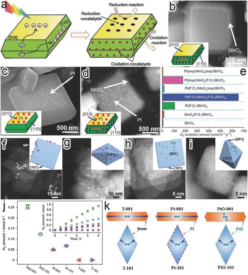
a) Schematic for selective deposition of reduction and oxidation cocatalysts on the {010} and {110} facets of BiVO4 based on the charge separation between different facets. b–d) SEM images and schematic illustration (inset) for (b) MnOx(P.D.)/BiVO4, (c) Pt(P.D.)/BiVO4, and (d) Pt(P.D.)/MnOx(P.D.)/BiVO4 hybrid structures. e) Photocatalytic water oxidation performance of BiVO4 based structures. Reproduced with permission.20, 93 Copyright 2013, Nature Publishing Group and Copyright 2014, Royal Society of Chemistry. f–i) TEM images and geometric models (inset) of (f) Pt‐001, (g) Pt‐101, (h) PtO‐001 and (i) PtO‐101. j) H2 evolution rates by bare TiO2 and TiO2 loaded with PtO clusters and metallic Pt cocatalyst, respectively. k) Schematic illustrating the migration of the photogenerated electrons in TiO2‐based photocatalysts. Reproduced with permission.121 Copyright 2015, Elsevier.
It is worth mentioning that the facet‐dependent charge accumulation relies on the migration distance of charge carriers to surface facets. In certain geometric shapes, the charge carriers may travel along significantly different lengths to various facets inside a semiconductor. A short migration distance can suppress electron‐hole recombination and facilitate charge accumulation at the facet, so interfacial charge transfer would be enhanced by selectively depositing a new component on the semiconductor facet with short charge traveling length. For instance, Pt and PtO reduction cocatalysts were deposited on the TiO2 nanosheets (T‐001) and octahedrons (T‐101) that were dominated with {001} and {101} facets, respectively, to form four different interfaces (namely, Pt‐001, Pt‐101, PtO‐001 and PtO‐101).121 As indicated by TEM analysis, the metallic Pt cocatalyst was preferentially anchored on the TiO2{101} facet, while the PtO could be stabilized on both {001} and {101} facets (Figure 14f–i). During the photocatalysis, the Pt‐101 exhibited higher activity than the Pt‐001 in H2 evolution, while the activity of PtO‐001 exceeded that of PtO‐101 (Figure 14j). In this system, the Pt‐101 and PtO‐001 shortened the electron migration path as compared with the Pt‐001 and PtO‐101, respectively (Figure 14k); the distance between the center of semiconductor and cocatalysts was ∼2 nm in PtO‐001, ∼25 nm in Pt‐001, and ∼12 nm in both PtO‐101 and Pt‐101. Although TiO2{101} was the reduction facet with electron accumulation by spatial charge separation (Figure 14k),86, 87, 88, 89, 90, 91, 92 the Pt‐101 with Pt selectively deposited on {101} exhibited the lowest photocatalytic activity. This case well demonstrates that both spatial charge separation and charge migration length should be taken into account in the interface facet design.
In the facet‐engineered interface design, the facet‐dependent electronic band structure in semiconductor is another key factor. It causes different energy band alignments on the formed interfaces and influences the efficiency of interfacial charge transfer. For instance, the work function of Cu2O{100} (ca. 7.2 eV) is much higher than that of Cu2O{111} (ca. 4.8 eV) in Cu2O cuboctahedrons,21 leading to the accumulation of electrons and holes on the {100} and {111} facet, respectively (Figure 15 a). To facilitate charge separation, a Schottky junction may be built between p‐type Cu2O and Pd to trap the photogenerated holes. Determined by spatial charge distribution, the Cu2O{111} facets with hole accumulation should be an ideal location to form Cu2O{111}‐Pd interface for hole trapping (Figure 15b). Unfortunately, the Schottky junction could not be formed at the Cu2O{111}‐Pd interface as Cu2O{111} has a lower work function than Pd (Figure 15c).11 In stark contrast, the higher work function of Cu2O{100} than Pd favored the establishment of Schottky barrier (Figure 15d). For this reason, the Pd‐decorated Cu2O cubes with Cu2O{100}‐Pd interface should be used for hole trapping instead (Figure 15e). As shown in Figure 15f, the hybrid structures between Cu2O cubes and Pd nanoparticles showed more prominent H2 production in comparison with other Cu2O counterparts.
Figure 15.
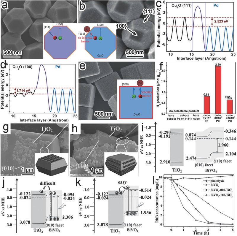
a) SEM image of Cu2O cuboctahedrons and schematic illustration (inset) for the charge spatial distribution between the {100} and {111} facet. b) SEM image of Cu2O cuboctahedrons with {111} surface decorated with Pd and schematic illustration (inset) for the charge transfer on the Cu2O{111}‐Pd interface. c) Potential lineup diagram for Cu2O{111}‐Pd interface obtained from first‐principles simulations. d) Potential lineup diagram for Cu2O{100}‐Pd interface obtained from first‐principles simulations. e) SEM image of {100}‐faceted Cu2O cubes decorated with Pd and schematic illustration (inset) for the charge transfer on the Cu2O{100}‐Pd interface. f) Photocatalytic hydrogen production from pure water by Cu2O‐based photocatalysts. Reproduced with permission.21 g,h) SEM images and schematic illustration (inset) of (g) BiVO4‐010‐TiO2 and (h) BiVO4‐110‐TiO2 heterojunctions. i–k) Relative energy band levels of (i) TiO2, BiVO4{010} facet, and BiVO4{110} facet, and (j,k) two types of BiVO4‐TiO2 heterojunctions with different contact facets. l) Photocatalytic activities of BiVO4‐based photocatalysts in RhB degradation under visible‐light irradiation. Reproduced with permission.122
Following a similar mechanism, the BiVO4‐TiO2 interfaces were designed for the flow of photogenerated electrons from BiVO4 to TiO2 under visible‐light irradiation.122 Selectively growing TiO2 on {010} and {110} facet of BiVO4, two different BiVO4‐TiO2 heterojunctions (namely, BiVO4‐010‐TiO2 and BiVO4‐110‐TiO2) were formed, respectively (Figure 15g,h). Due to the lower CBM and VBM of BiVO4{010} than BiVO4{110}, the BiVO4{010}‐TiO2 interface exhibited a higher interfacial CB energy barrier as compared with BiVO4{110}‐TiO2 interface (Figure 15i–k). This feature hindered the electron transfer from BiVO4{010} to TiO2. As a result, the BiVO4‐110‐TiO2 heterojunction exhibited higher photocatalytic performance in RhB degradation (Figure 15l).
The third factor for facet‐dependent interfacial charge transfer is associated with the correlation of interfacial structural and electronic couplings with facet contacts. Based on this correlation, we have designed a Ag‐BiOCl‐Pd hybrid structure for synergizing the interfacial charge transfer of plasmonic metal‐semiconductor (Ag‐BiOCl) with semiconductor‐metal (BiOCl‐Pd) Schottky junctions.22 In a plasmonic metal‐semiconductor interface, the injection of plamsonic hot carriers to semiconductor follows an opposite direction to the charge trapping by metal through the Schottky junction.123, 124 In our design, two different metal‐semiconductor interfaces were established to circumvent this undesired situation, in which the semiconductor facets and metals were rationally selected for the plasmonic effect and Schottky junction, respectively.
The design begins with the facet‐dependent charge distribution in p‐type BiOCl nanoplates (Figure 16 a). The photogenerated holes and electrons are preferentially accumulated on four side {110} and top/bottom {001} facets, respectively (Figure 16b). Based on this spatial charge separation, two interfaces were designed. The first interface was formed between BiOCl{001} and plasmonic Ag, where the Ag injected hot holes into BiOCl under visible‐light illumination. The other interface was formed between BiOCl{110} and nonplasmonic Pd to establish the Schottky barrier so that the holes can be trapped by the Pd. To prove the rationality of the design, we have investigated the charge transfer of the two interfaces. At the Ag{100}‐{001}BiOCl interface, the plasmonic hot holes in Ag generated by visible light were injected into BiOCl, while the Ag could not effectively trap the holes from the UV‐photoexcited BiOCl through a Schottky junction (Figure 16c). The key to this interface was the thick contact barrier layer (3.0 Å), which disfavored the migration of photoexcited holes from BiOCl{001} to Ag but did not bother the injection of plasmonic hot holes into the VB of BiOCl (Figure 16d). At the other BiOCl{110}‐Pd{100} interface, the interfacial barrier layer was thin enough (1.1 Å) to allow efficient hole trapping through the Schottky junction under UV‐light irradiation (Figure 16e–h). To integrate the two interfaces, Ag‐{001}BiOCl{110}‐Pd hybrid structure was fabricated by selectively depositing Ag and Pd nanocubes on the {001} and {110} facets of BiOCl, respectively (Figure 16i). The synergetic effect of Ag{100}‐{001}BiOCl and BiOCl{110}‐Pd{100} interfaces offerred the highest photocatalytic performance in O2 evolution under full‐spectrum irradiation (Figure 16j). In this Ag‐{001}BiOCl{110}‐Pd ternary structure, the two interfaces steered the charge flow through three effects – the plasmonic deep hole injection from Ag through the Ag{100}‐{001}BiOCl interface, the intrinsic facet‐dependent spatial charge separation inside the BiOCl, and the Schottky junction with Pd to extract holes from BiOCl through the BiOCl{110}‐Pd{100} interface (Figure 16k).
Figure 16.
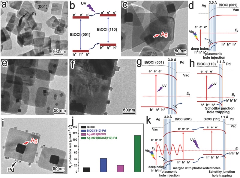
a) TEM image of BiOCl nanoplates. b) Schematic illustration showing the facet‐dependent charge migration in BiOCl. c) TEM image of Ag‐{001}BiOCl. d) Schematic illustration for energy band alignment and hole carrier migration at Ag{100}‐BiOCl{001} interface. e,f) TEM images of (e) BiOCl{001}‐Pd and (f) BiOCl{110}‐Pd. g,h) Schematic illustration for energy band alignment and hole carrier migration at (g) BiOCl{001}‐Pd{100} interface and (h) BiOCl{110}‐Pd{100} interface. i) TEM image of Ag‐{001}BiOCl{110}‐Pd hybrid structure. j) Photocatalytic O2 evolution from water by BiOCl‐based materials under full‐spectrum irradiation. k) Schematic illustrating the band alignment and charge flow at two metal‐semiconductor interfaces in Ag‐{001}BiOCl{110}‐Pd under full‐spectrum irradiation. Reproduced with permission.22
Certainly the facet‐engineered interface design is not limited in the selection of semiconductor facets in defining the interface. The facets of other components (e.g., metal) can also be tailored to promote interfacial charge transfer. The metal possesses facet‐dependent work function, altering the interfacial band alignment with semiconductor. For instance, the Eosin Y (EY)‐sensitized Pt/TiO2(P25) samples with different exposed facets (e.g., {100}, {100/111}, and {111}) of Pt were employed as photocatalysts for H2 evolution under visible‐light irradiation.120 The EY‐Pt{111}/TiO2 photocatalyst exhibited higher activity than EY‐Pt{100}/TiO2 and EY‐Pt{100/111}/TiO2 (Figure 17 a), as the higher Fermi level of Pt{111} enabled larger difference with the CB of TiO2 promoting the electron trapping on Pt{111} (Figure 17b).
Figure 17.
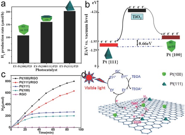
a) Photocatalytic H2 evolution rate from triethanolamine (TEOA) aqueous solution on EY‐TiO2‐Pt{100}, EY‐TiO2‐Pt{100/111}, and EY‐TiO2‐Pt{111} under visible‐light irradiation. b) Energy band diagrams for Pt{100} (dotted curve) and Pt{111} facets (solid curve) relative to TiO2. Reproduced with permission.120 Copyright 2013, American Chemical Society. c) H2 evolution from EY‐photosensitized systems catalyzed by RGO, Pt{100}, Pt{111}, Pt{100}/RGO, and Pt{111}/RGO. d) Proposed photocatalytic mechanism for hydrogen evolution over Pt{100}/RGO and Pt{111}/RGO cocatalysts under visible‐light irradiation. Reproduced with permission.125 Copyright 2015, American Chemical Society.
Moreover, the interfacial coupling tuned by metal facets may affect the efficiency of charge transfer. In the case of EY‐sensitized Pt/reduced graphene oxide (rGO), different exposed facets of Pt (e.g., Pt{100}/rGO and Pt{111}/rGO) were integrated with the rGO as visible‐light photocatalysts. The photoinduced electrons were transfered to Pt cocatalysts across the rGO‐Pt interface for H2 evolution.125 The H2 evolution activity by Pt{100}/rGO turned out to be substantially higher than that of Pt{111}/rGO, despite the superior performance of bare Pt{111} to Pt{100} (Figure 17c). This performance turnover was caused by the stronger interaction between Pt{100} and rGO, resulting in faster charge transfer at the rGO‐Pt{100} interface (Figure 17d). In general, facet‐engineered design has been carried out for various interfaces of photocatalysts, in efforts to trap charges for redox reactions or extract charges from light‐sensitized components (e.g., plasmonic metal, and semiconductor sensitizer). The comparison of interfacial charge transfer efficiency with different facet contacts in various photocatalytic hybrid materials has been summarized in Table 3 .
Table 3.
Efficiency of interfacial charge transfer with different facet contacts in various photocatalytic hybrid materials as well as their corresponding mechanisms
| Photocatalytic hybrid materials | Type of charge transfer | Comparison of efficiency in interfacial charge transfer | Mechanism | Ref. |
|---|---|---|---|---|
| Pt‐BiVO4‐MnOx | Charge trapping | Pt‐{010}BiVO4{110}‐MnOx > Pt‐{010}/{110}BiVO4{010}/{110}‐MnOx | Facet‐dependent charge accumulation | 20 |
| TiO2‐PtO | Charge trapping | TiO2{001}‐PtO > TiO2{101}‐PtO | Facet‐dependent charge accumulation | 121 |
| Cu2O‐Pd | Charge trapping | Cu2O{100}‐Pd > Cu2O{111}‐Pd | Different energy band alignments | 21 |
| BiVO4‐TiO2 | Charge injection | BiVO4{110}‐TiO2 > BiVO4{010}‐TiO2 | Different energy band alignments | 122 |
| BiOCl‐Pd | Charge trapping | BiOCl{110}‐Pd{100} > BiOCl{001}‐Pd{100} | Different interfacial couplings | 22 |
| TiO2‐Pt | Charge trapping | TiO2‐Pt{111} > TiO2‐Pt{100} | Different energy band alignments | 120 |
| Graphene‐Pt | Charge trapping | Graphene‐Pt{100} > graphene‐Pt{111} | Different interfacial couplings | 125 |
| TiO2‐Pt | Charge trapping | TiO2{001}‐Pt > TiO2{010}‐Pt | Different interfacial couplings | 115 |
| Au‐BiOCl | Hot charge injection | Au‐BiOCl{010} > Au‐BiOCl{001} | Different energy band alignments | 42 |
| TiO2‐graphene | Charge trapping | TiO2{100}‐graphene > TiO2{101}‐graphene > TiO2{001}‐graphene | Different interfacial couplings | 43 |
| Cu2WS4‐Pt | Charge trapping | Cu2WS4{101}‐Pt > Cu2WS4{001}‐Pt | Different energy band alignments | 49 |
| PbTiO3‐Pt | Charge trapping | PbTiO3 positively charged {001}‐Pt > PbTiO3 positively/negatively charged {001}‐Pt | Facet‐dependent charge accumulation | 52 |
| Cu2O‐Pd | Charge trapping | Cu2O{100}‐Pd{100} > Cu2O{100}‐Pd(without determined facet of Pd) | Different interfacial couplings | 58 |
| Au‐Cu2O‐Co3O4 | Charge trapping | Au‐{100}Cu2O{111}‐Co3O4 > Au‐{111}Cu2O{111}‐Co3O4 | Facet‐dependent charge accumulation | 107 |
| TiO2‐C3N4 | Charge injection | TiO2{101}‐C3N4 > TiO2{001}‐C3N4 | Facet‐dependent charge accumulation | 126 |
| Cu2O‐graphene | Charge trapping | Cu2O{111}‐graphene > Cu2O{110}‐graphene > Cu2O{100}‐graphene | Different interfacial couplings | 127 |
| K2La2Ti3O10‐Ni | Charge trapping | K2La2Ti3O10{101}‐Ni{111} > K2La2Ti3O10{002}‐Ni{111} | Different interfacial couplings | 128 |
6. Conclusions and Perspectives
Facet‐engineered surface and interface design of photocatalytic materials represents an interesting and important development direction toward enhanced photocatalytic performance. Thereinto, the facet‐engineered surface design has been carried out for both mono‐component and multi‐component photocatalytic structures, in efforts to enhance surface catalytic reactions by controlling the exposed facets of catalytic components. Three key factors are responsible for the dependence of surface reaction activity on the exposed facets: 1) the adsorption and activation of reactants on surface facets; 2) the surface electronic band structures of various facets determining the redox abilities of photogenerated charge carriers; and 3) accumulation of photogenerated electrons or holes on different facets.
Meanwhile, the facet‐engineered interface design has implemented for the interface between light‐harvesting and catalytic components in multi‐component hybrid structures, which can promote interfacial charge transfer by tailoring the contact facets. The efficiency of interfacial charge transfer is manuevered by contact facets due to three main reasons: 1) the accumulation of photogenerated electrons or holes on the facets that form the interface; 2) the interfacial energy band alignment depending on the surface state structures of different facets; 3) the interfacial structural and electronic couplings relying on the facet contacts.
Based on the fundamental understanding, facet adjustment has been performed for the surface and interface of photocatalytic materials through various synthetic methods. The use of facet‐selective capping agent, kinetic control, thermodynamic control, and anisotropic etching have been developed for tailoring the exposed facets on surface. In comparison, the facet engineering for interface structures is relatively challenging. Thus far, limited success has been made by employing facet‐selective capping agents, facet‐dependent photodeposition, and facet‐dependent selective adsorption. It is anticipated that more efforts will be made toward the interface engineering in the future.
Enabled by the well‐established techniques for surface control, the photocatalytic efficiency for mono‐component semiconductor structures has been significantly improved through either increasing the percentage of the surface facets with high catalytic activity or optimizing the ratio of different facets in synergistic effects. As for multi‐component hybrid structures, the enhancement on photocatalytic performance has been mainly achieved by following the same strategy as bare semiconductors – rationally exposing the component facet with high catalytic activity on surface. The other important factor for hybrid structures – effciency of interfacial charge transfer – has been optimized to some extent by selecting appropriate facets for interface formation; however, it is still a long way to go along this development direction.
Although some encouraging advances have been achieved for the facet‐engineered surface and interface design of photocatalytic materials in the recent years, it still remains a grand challenge to fully exert the functions of facet engineering to photocatalysis. In our opinion, the most challenging task is to control the material interface inside a multiple‐component hybrid structure. This challenge not only originates from the limited synthetic techniques for controlling the interfacial facets, but also requires advanced characterization techniques to probe the charge kinetics at the interface.
In terms of the synthesis, the formation of many interface structures suffers from the large lattice mismatch between components, reducing the interfacial structural and electronic couplings. To overcome the interfacial strain induced by lattice mismatch, non‐epitaxial growth should be a promising approach. In this growth scheme, the nucleation and growth require that the existing component can provide the sites with strong binding to the newly formed one. From the success in literature (e.g., Pd‐Cu2O and TiO2‐Pd), chemical bondings such as Pd–O can make an important contribution to the non‐epitaxial growth. Another limitation lies on the fact that morphology‐controlling agents are still commonly involved in the existing synthetic methods. The presence of capping agents on component surface will inevitably compromise the quality of interface structures. As for the mechanism research, the characterization techniques at high spatial, spectral and temporal resolutions are highly desirable for probing the interfacial charge kinetics and enabling deeper understanding on the facet‐dependent photocatalytic behaviors. Furthermore, modern theoretical simulations and calculations are also required to raise the level of understanding on the facet effect on photocatalysis and to provide guidance for the facet engineering toward the design of photocatalytic materials. Taken together, the research at the intersection of precise syntheses, advanced characterizations and theoretical simulations can help establish the relationship between facet structure and photocatalytic performance,11, 129, 130 which will in turn formulate well‐designed surface and interface facets for highly efficient photocatalysts.
Acknowledgements
This work was financially supported by the 973 Program (No. 2014CB848900), NSFC (No. 21471141, U1532135), Recruitment Program of Global Experts, CAS Hundred Talent Program, Fundamental Research Funds for the Central Universities (No. WK2060190025, WK2310000035), Hefei Science Center CAS (No. 2015HSC‐UP009), Zhejiang Provincial Natural Science Foundation (No. LQ16B010001), Open Research Fund of Top Key Discipline of Chemistry in Zhejiang Provincial Colleges, and Key Laboratory of the Ministry of Education for Advanced Catalysis Materials (Zhejiang Normal University) (ZJHX201507).
Biographies
Song Bai received his B.S. and M.S. degrees from the Jiangsu University in 2009 and 2012, respectively. In 2015, he obtained his Ph.D. degree with Professor Yujie Xiong from the University of Science and Technology of China (USTC), and started as an assistant Professor in Zhejiang Normal University. His research interests focus on the design and synthesis of novel hybrid nanomaterials for photocatalysis.

Lili Wang received her B.S. in chemistry from the Huaibei Normal University in 2011. She is currently a Ph.D. student under the tutelage of Professor Yujie Xiong. Her research interests focus on the design and synthesis of photocatalytic materials.

Zhengquan Li received his B.S. in chemistry from Anhui University in 2000 and Ph.D in inorganic chemistry from University of Science and Technology of China in 2005. After postdoctoral trainings at National University of Singapore and Washington University in St. Louis, he joined Zhejiang Normal University as a special‐term professor in 2009. His current research interests focus on the synthesis and application of lanthanide‐based nanomaterials.

Yujie Xiong received his B.S. in chemical physics in 2000 and Ph.D. in inorganic chemistry in 2004 (with Professor Yi Xie), both from the University of Science and Technology of China (USTC). After four‐year training with Professors Younan Xia and John A. Rogers, he joined the NSF‐NNIN at Washington University in St. Louis as the Principal Scientist and Lab Manager. Starting from 2011, he is a Professor of Chemistry at the USTC. He has published more than 120 papers with over 10,000 citations (H‐index 48). His research interests include the synthesis, fabrication and assembly of inorganic materials for energy and environmental applications.

Bai S., Wang L., Li Z., Xiong Y., Adv. Sci. 2017, 4, 1600216.
Contributor Information
Song Bai, Email: songbai@zjnu.edu.cn.
Yujie Xiong, Email: yjxiong@ustc.edu.cn.
References
- 1. Linsebigler A. L., Lu G., Yates J. T., Chem. Rev. 1995, 95, 735. [Google Scholar]
- 2. Chen X., Chen S., Guo L., Mao S. S., Chem. Rev. 2010, 110, 6503. [DOI] [PubMed] [Google Scholar]
- 3. Hoffmann M. R., Martin S. T., Choi W., Bahnemannt D. W., Chem. Rev. 1995, 95, 69. [Google Scholar]
- 4. Kudo A., Miseki Y., Chem. Soc. Rev. 2009, 38, 253. [DOI] [PubMed] [Google Scholar]
- 5. Schneider J., Matsuoka M., Takeuchi M., Zhang J., Horiuchi Y., Anpo M., Bahnemann D. W., Chem. Rev. 2014, 114, 9919. [DOI] [PubMed] [Google Scholar]
- 6. Habisreutinger S. N., Schmidt‐Mende L., Stolarczyk J. K., Angew. Chem. Int. Ed. 2013, 52, 7372. [DOI] [PubMed] [Google Scholar]
- 7. Tong H., Ouyang S., Bi Y., Umezawa N., Oshikiri M., Ye J., Adv. Mater. 2012, 24, 229. [DOI] [PubMed] [Google Scholar]
- 8. Ma Y., Wang X., Jia Y., Chen X., Han H., Li C., Chem. Rev. 2014, 114, 9987. [DOI] [PubMed] [Google Scholar]
- 9. Tu W., Zou Y., Zhou Z., Adv. Mater. 2014, 26, 4607. [DOI] [PubMed] [Google Scholar]
- 10. Gellman A. J., Shukla N., Nat. Mater. 2009, 8, 87. [DOI] [PubMed] [Google Scholar]
- 11. Bai S., Jiang J., Zhang Q., Xiong Y., Chem. Soc. Rev. 2015, 44, 2893. [DOI] [PubMed] [Google Scholar]
- 12. Qu Y., Duan X., Chem. Soc. Rev. 2013, 42, 2568. [DOI] [PubMed] [Google Scholar]
- 13. Bai S., Xiong Y., Chem. Commun. 2015, 51, 10261. [DOI] [PubMed] [Google Scholar]
- 14. Bai S., Jiang W., Li Z., Xiong Y., ChemNanoMat 2015, 1, 223. [Google Scholar]
- 15. Zhou K., Li Y., Angew. Chem. Int. Ed. 2012, 51, 602. [DOI] [PubMed] [Google Scholar]
- 16. Liu G., Yu J. C., Lu G. Q., Cheng H. M., Chem. Commun. 2011, 47, 6763. [DOI] [PubMed] [Google Scholar]
- 17. Xu H., Reunchan P., Ouyang S., Tong H., Umezawa N., Kako T., Ye J., Chem. Mater. 2013, 25, 405. [Google Scholar]
- 18. Jiang J., Zhao K., Xiao X., Zhang L., J. Am. Chem. Soc. 2012, 134, 4473. [DOI] [PubMed] [Google Scholar]
- 19. Wu N., Wang J., Tafen D. N., Wang H., Zheng J. G., Lewis J. P., Liu X., Leonard S. S., Manivannan A., J. Am. Chem. Soc. 2010, 132, 6679. [DOI] [PMC free article] [PubMed] [Google Scholar]
- 20. Li R., Zhang F., Wang D., Yang J., Li M., Zhu J., Zhou X., Fan H., Li C., Nat. Commun. 2013, 4, 1432. [DOI] [PubMed] [Google Scholar]
- 21. Wang L., Ge J., Wang A., Deng M., Wang X., Bai S., Li R., Jiang J., Zhang Q., Luo Y., Xiong Y., Angew. Chem. Int. Ed. 2014, 53, 5107. [DOI] [PubMed] [Google Scholar]
- 22. Bai S., Li X., Kong Q., Long R., Wang C., Jiang J., Xiong Y., Adv. Mater. 2015, 27, 3444. [DOI] [PubMed] [Google Scholar]
- 23. Kuang Q., Wang X., Jiang Z., Xie Z., Zheng L., Acc. Chem. Res. 2014, 47, 308. [DOI] [PubMed] [Google Scholar]
- 24. Xia Y., Xiong Y., Lim B., Skrabalak S. E., Angew. Chem. Int. Ed. 2009, 48, 60. [DOI] [PMC free article] [PubMed] [Google Scholar]
- 25. Liu G., Yang H. G., Pan J., Yang Y. Q., Lu G. Q., Cheng H. M., Chem. Rev. 2014, 114, 9559. [DOI] [PubMed] [Google Scholar]
- 26. Long R., Zhou S., Wiley B. J., Xiong Y., Chem. Soc. Rev. 2014, 43, 6288. [DOI] [PubMed] [Google Scholar]
- 27. Wu B., Zheng N., Nano Today 2013, 8, 168. [Google Scholar]
- 28. Xiong Y., Xia Y., Adv. Mater. 2007, 19, 3385. [Google Scholar]
- 29. Zhang D. F., Zhang H., Guo L., Zheng K., Han X. D., Zhang Z., J. Mater. Chem. 2009, 19, 5220. [Google Scholar]
- 30. Guan M., Xiao C., Zhang J., Fan S., An R., Cheng Q., Xie J., Zhou M., Ye B., Xie Y., J. Am. Chem. Soc. 2013, 135, 10411. [DOI] [PubMed] [Google Scholar]
- 31. Chen M., Wu B., Yang J., Zheng N., Adv. Mater. 2012, 24, 862. [DOI] [PubMed] [Google Scholar]
- 32. Pan J., Liu G., Lu G. Q., Cheng H. M., Angew. Chem. Int. Ed. 2011, 50, 2133. [DOI] [PubMed] [Google Scholar]
- 33. Han X., Kuang Q., Jin M., Xie Z. X., Zheng L., J. Am. Chem. Soc. 2009, 131, 3152. [DOI] [PubMed] [Google Scholar]
- 34. Wang Y., He J., Liu C., Chong W. H., Chen H., Angew. Chem. Int. Ed. 2015, 54, 2022. [DOI] [PubMed] [Google Scholar]
- 35. Wang X., Wu H. F., Kuang Q., Huang R. B., Xie Z. X., Zheng L. S., Langmuir 2010, 26, 2774. [DOI] [PubMed] [Google Scholar]
- 36. Lin H. X., Lei Z. C., Jiang Z. Y., Hou C. P., Liu D. Y., Xu M. M., Tian Z. Q., Xie Z. X., J. Am. Chem. Soc. 2013, 135, 9311. [DOI] [PubMed] [Google Scholar]
- 37. Ouyang J., Pei J., Kuang Q., Xie Z., Zheng L., ACS Appl. Mater. Interfaces 2014, 6, 12505. [DOI] [PubMed] [Google Scholar]
- 38. Liu L., Zhuang Z., Xie T., Wang Y. G., Li J., Peng Q., Li Y., J. Am. Chem. Soc. 2009, 131, 16423. [DOI] [PubMed] [Google Scholar]
- 39. Huang Z., Geyer N., Werner P., Boor J., Gosele U., Adv. Mater. 2011, 23, 285. [DOI] [PubMed] [Google Scholar]
- 40. Han X. G., Jiang Y. Q., Xie S. F., Kuang Q., Zhou X., Cai D. P., Xie Z. X., Zheng L. S., J. Phys. Chem. C 2010, 114, 10114. [Google Scholar]
- 41. Yamada Y., Tsung C. K., Huang W., Huo Z., Habas S. E., Soejima T., Aliaga C. E., Somorjai G. A., Yang P., Nat. Chem. 2011, 3, 372. [DOI] [PubMed] [Google Scholar]
- 42. Liu G., Wang T., Zhou W., Meng X., Zhang H., Liu H., Kako T., Ye J., J. Mater. Chem. C 2015, 3, 7538. [Google Scholar]
- 43. Liu L., Liu Z., Liu A., Gu X., Ge C., Gao F., Dong L., ChemSusChem 2014, 7, 618. [DOI] [PubMed] [Google Scholar]
- 44. Bai S., Xie M., Kong Q., Jiang W., Qiao R., Li Z., Jiang J., Xiong Y., Part. Part. Syst. Charact. DOI: 10.1002/ppsc.201500239. [Google Scholar]
- 45. Kuo C. H., Hua T. E., Huang M. H., J. Am. Chem. Soc. 2009, 131, 17871. [DOI] [PubMed] [Google Scholar]
- 46. Meir N., Plante I. J. L., Flomin K., Chockler E., Moshofsky B., Diab M., Volokh M., Mokari T., J. Mater. Chem. A 2013, 1, 1763. [Google Scholar]
- 47. Niu M., Huang F., Cui L., Huang P., Yu Y., Wang Y., ACS Nano 2010, 4, 681. [DOI] [PubMed] [Google Scholar]
- 48. Read C. G., Steinmiller E. M. P., Choi K. S., J. Am. Chem. Soc. 2009, 131, 12040. [DOI] [PubMed] [Google Scholar]
- 49. Wang B., Liu M., Zhou Z. H., Guo L., Adv. Sci. 2015, 2, 1500153. [DOI] [PMC free article] [PubMed] [Google Scholar]
- 50. Li L., Salvador P. A., Rohrer G. S., Nanoscale 2014, 6, 24. [DOI] [PubMed] [Google Scholar]
- 51. Giocondi J. L., Rohrer G. S., J. Phys. Chem. B 2001, 105, 8275. [Google Scholar]
- 52. Zhen C., Yu J. C., Liu G., Cheng H. M., Chem. Commun. 2014, 50, 10416. [DOI] [PubMed] [Google Scholar]
- 53. Yu Z. B., Xie Y. P., Liu G., Lu G. Q., Ma X. L., Cheng H. M., J. Mater. Chem. A 2013, 1, 2773. [Google Scholar]
- 54. Wenderich K., Klaassen A., Siretanu I., Mugele F., Mul G., Angew. Chem. Int. Ed. 2014, 53, 12476. [DOI] [PubMed] [Google Scholar]
- 55. Bai S., Yang L., Wang C., Lin Y., Lu J., Jiang J., Xiong Y., Angew. Chem. Int. Ed. 2015, 54, 14810. [DOI] [PubMed] [Google Scholar]
- 56. Bai S., Wang C., Deng M., Gong M., Bai Y., Jiang J., Xiong Y., Angew. Chem. Int. Ed. 2014, 53, 12120. [DOI] [PubMed] [Google Scholar]
- 57. Fu Q., Yang F., Bao X., Acc. Chem. Res. 2013, 46, 1692. [DOI] [PubMed] [Google Scholar]
- 58. Bai S., Ge J., Wang L., Gong M., Deng M., Kong Q., Song L., Jiang J., Zhang Q., Luo Y., Xie Y., Xiong Y., Adv. Mater. 2014, 26, 5689. [DOI] [PubMed] [Google Scholar]
- 59. Zhou Z. Y., Tian N., Li J. T., Broadwell I., Sun S. G., Chem. Soc. Rev. 2011, 40, 4167. [DOI] [PubMed] [Google Scholar]
- 60. Li C., Koenigsmann C., Ding W., Rudshteyn B., Yang K. R., Regan K. P., Konezny S. J., Batista V. S., Brudvig G. W., Schmuttenmaer C. A., Kim J. H., J. Am. Chem. Soc. 2015, 137, 1520. [DOI] [PubMed] [Google Scholar]
- 61. Bi Y., Ouyang S., Umezawa N., Cao J., Ye J., J. Am. Chem. Soc. 2011, 133, 6490. [DOI] [PubMed] [Google Scholar]
- 62. Liu B., Ma L., Ning L. C., Zhang C. J., Han G. P., Pei C. J., Zhao H., Liu S. Z., Yang H. Q., ACS Appl. Mater. Interfaces 2015, 7, 6109. [DOI] [PubMed] [Google Scholar]
- 63. He H., Yin J., Li Y., Zhang Y., Qiu H., Xu J., Xu T., Wang C., Appl. Catal. B:Environ. 2014, 156–157, 35. [Google Scholar]
- 64. Mclaren A., Valdes‐Solis T., Li G., Tsang S. C., J. Am. Chem. Soc. 2009, 131, 12540. [DOI] [PubMed] [Google Scholar]
- 65. Ho J. Y., Huang M. H., J. Phys. Chem. C 2009, 113, 14159. [Google Scholar]
- 66. Zhao X., Jin W., Cai J., Ye J., Li Z., Ma Y., Xie J., Qi L., Adv. Funct. Mater. 2011, 21, 3554. [Google Scholar]
- 67. Ye L., Mao J., Peng T., Zan L., Zhang Y., Phys. Chem. Chem. Phys. 2014, 16, 15675. [DOI] [PubMed] [Google Scholar]
- 68. Huang W. C., Lyu L. M., Yang Y. C., Huang M. H., J. Am. Chem. Soc. 2012, 134, 1261. [DOI] [PubMed] [Google Scholar]
- 69. Wang H., Yang J., Li X., Zhang H., Li J., Guo L., Small 2012, 8, 2802. [DOI] [PubMed] [Google Scholar]
- 70. Wang G., Ma X., Huang B., Cheng H., Wang Z., Zhan J., Qin X., Zhang X., Dai Y., J. Mater. Chem. 2012, 22, 21189. [Google Scholar]
- 71. Harn Y. W., Yang T. H., Tang T. Y., Chen M. C., Wu J. M., ChemCatChem 2015, 7, 80. [Google Scholar]
- 72. Pan M., Zhang H., Gao G., Liu L., Chen W., Environ. Sci. Technol. 2015, 49, 6240. [DOI] [PubMed] [Google Scholar]
- 73. Martin D. J., Umezawa N., Chen X., Ye J., Tang J., Energy Envion. Sci. 2013, 6, 3380. [Google Scholar]
- 74. Lin W., Wang X., Wang Y., Zhang J., Lin Z., Zhang B., Huang F., Chem. Commun. DOI: 10.1039/C3CC41498A. [Google Scholar]
- 75. Wu D., Wang B., Wang W., An T., Li G., Ng T. W., Yip H. Y., Xiong C., Lee H. K., Wong P. K., J. Mater. Chem. A 2015, 3, 15148. [Google Scholar]
- 76. Wang X., Liu M., Zhou Z., Guo L., J. Phys. Chem. C 2015, 119, 20555. [Google Scholar]
- 77. Roca R. A., Sczancoski J. C., Nogueira I. C., Fabbro M. T., Alves H. C., Gracia L., Santos L. P. S., de Sousa C. P., Andres J., Luz G. E., Longo E., Cavalcante L. S., Catal. Sci. Technol. 2015, 5, 4091. [Google Scholar]
- 78. Weng S., Pei Z., Zheng Z., Hu J., Liu P., ACS Appl. Mater. Interfaces 2013, 5, 12380. [DOI] [PubMed] [Google Scholar]
- 79. Jiang D., Wang W., Zhang L., Zheng Y., Wang Z., ACS Catal. 2015, 5, 4851. [Google Scholar]
- 80. Li J., Bai H., Yi W., Liu J., Li Y., Zhang Q., Yang H., Xi G., Nano Res. 2016, 9, 1523. [Google Scholar]
- 81. Kimijima T., Kanie K., Nakaya M., Muramatsu A., Appl. Catal. B:Environ. 2014, 144, 462. [Google Scholar]
- 82. Wang H., Lang X., Hao R., Guo L., Li J., Wang L., Han X., Nano Energy 2016, 19, 8. [Google Scholar]
- 83. Zhang H., Lu Y., Liu H., Fang J., Nanoscale 2015, 7, 11591. [DOI] [PubMed] [Google Scholar]
- 84. Zhang H., Yang Y., Zhou Z., Zhao Y., Liu L., J. Phys. Chem. C 2014, 118, 14662. [Google Scholar]
- 85. Pasternak S., Paz Y., ChemPhysChem 2013, 14, 2059. [DOI] [PubMed] [Google Scholar]
- 86. Liu C., Han X., Xie S., Kuang Q., Wang X., Jin M., Xie Z., Zheng L., Chem. Asian J. 2013, 8, 282. [DOI] [PubMed] [Google Scholar]
- 87. Ye L., Liu J., Tian L., Peng T., Zan L., Appl. Catal. B:Environ. 2013, 134–135, 60. [Google Scholar]
- 88. Yu J., Low J., Xiao W., Zhou P., Jaroniec M., J. Am. Chem. Soc. 2014, 136, 8839. [DOI] [PubMed] [Google Scholar]
- 89. Murakami N., Kurihara Y., Tsubota T., Ohno T., J. Phys. Chem. C 2009, 113, 3062. [Google Scholar]
- 90. Zhang P., Tachikawa T., Bian Z., Majima Z., Appl. Catal. B:Environ. 2015, 176–177, 678. [Google Scholar]
- 91. Wang X., Li R., Xu Q., Han H., Li C., Acta Phys. ‐Chim. Sin. 2013, 29, 1566. [Google Scholar]
- 92. Zheng Z., Huang B., Lu J., Qin X., Zhang X., Dai Y., Chem. Eur. J. 2011, 17, 15032. [DOI] [PubMed] [Google Scholar]
- 93. Li R., Han H., Zhang F., Wang D., Li C., Energy Envion. Sci. 2014, 7, 1369. [Google Scholar]
- 94. Liu T., Zhou X., Dupuisc M., Li C., Phys. Chem. Chem. Phys. 2015, 17, 23503. [DOI] [PubMed] [Google Scholar]
- 95. Zhu J., Fan F., Chen R., An H., Feng Z., Li C., Angew. Chem. Int. Ed. 2015, 54, 9111. [DOI] [PubMed] [Google Scholar]
- 96. Zhang L., Wang W., Sun S., Jiang D., Gao E., Appl. Catal. B:Environ. 2015, 162, 470. [Google Scholar]
- 97. Li P., Zhou Y., Zhao Z., Xu Q., Wang X., Xiao M., Zou Z., J. Am. Chem. Soc. 2015, 137, 9547. [DOI] [PubMed] [Google Scholar]
- 98. Li N., Liu M., Zhou Z., Zhou J., Sun Y., Guo L., Nanoscale 2014, 6, 9695. [DOI] [PubMed] [Google Scholar]
- 99. Lin H., Li L., Zhao M., Huang X., Chen X., Li G., Yu R., J. Am. Chem. Soc. 2012, 134, 8328. [DOI] [PubMed] [Google Scholar]
- 100. Ohno T., Sarukawa K., Matsumura M., New J. Chem. 2002, 26, 1167. [Google Scholar]
- 101. Roy N., Sohn Y., Pradhan D., ACS Nano 2013, 7, 2532. [DOI] [PubMed] [Google Scholar]
- 102. Xing M. Y., Yang B. X., Yu H., Tian B. Z., Bagwasi S., Zhang J. L., Gong X. Q., J. Phys. Chem. Lett. 2013, 4, 3910. [Google Scholar]
- 103. Wang B., Chen S., Guo L., Appl. Catal. B:Environ. 2015, 166–167, 320. [Google Scholar]
- 104. Wang B., Chen S., Guo L., ChemCatChem 2016, 8, 798. [Google Scholar]
- 105. Iizuka K., Wato T., Miseki Y., Saito K., Kudo A., J. Am. Chem. Soc. 2011, 133, 20863. [DOI] [PubMed] [Google Scholar]
- 106. Miseki Y., Kato H., Kudo A., Energy Environ. Sci. 2009, 2, 306. [Google Scholar]
- 107. Li G., Tao X., Chen R., Fan F., Li C., Chem. Eur. J. 2015, 21, 14337. [DOI] [PubMed] [Google Scholar]
- 108. Zhang L., Shi J., Liu M., Jing D., Guo L., Chem. Commun. 2014, 50, 192. [DOI] [PubMed] [Google Scholar]
- 109. Mei L., Zhao H., Lu B., Adv. Sci. 2015, 2, 1500116. [DOI] [PMC free article] [PubMed] [Google Scholar]
- 110. Gu L., Wang J., Cheng H., Zhao Y., Liu L., Han X., ACS Appl. Mater. Interfaces 2013, 5, 3085. [DOI] [PubMed] [Google Scholar]
- 111. Jiang B., Tian C., Pan Q., Jiang Z., Wang J. Q., Yan W., Fu H., J. Phys. Chem. C 2011, 115, 23718. [Google Scholar]
- 112. Sun J., Zhang H., Guo L. H., Zhao L., ACS Appl. Mater. Interfaces 2013, 5, 13035. [DOI] [PubMed] [Google Scholar]
- 113. Tang C., Liu E., Fan J., Hu X., Ma Y., Wan J., RSC Adv. 2015, 5, 91979. [Google Scholar]
- 114. Li Q., Zhao X., Yang J., Jiang C. J., Jin Z., Fan W., Nanoscale 2015, 7, 18971. [DOI] [PubMed] [Google Scholar]
- 115. Mao J., Ye L., Li K., Zhang X., Liu J., Peng T., Zan L., Appl. Catal. B:Environ. 2014, 144, 855. [Google Scholar]
- 116. Yang J., Wang D., Han H., Li C., Acc. Chem. Res. 2013, 46, 1900. [DOI] [PubMed] [Google Scholar]
- 117. Bai S., Yin W. J., Wang L., Li Z., Xiong Y., RSC Adv. 2016, 6, 57446. [Google Scholar]
- 118. Bai S., Wang X., Hu C., Xie M., Jiang J., Xiong Y., Chem. Commun. 2014, 50, 6094. [DOI] [PubMed] [Google Scholar]
- 119. Kovacs G., Fodor S., Vulpoi A., Schrantz K., Dombi A., Hernadi K., Danciu V., Pap Z., Baia L., J. Catal. 2015, 325, 156. [Google Scholar]
- 120. Cui E., Lu G., J. Phys. Chem. C 2013, 117, 26415. [Google Scholar]
- 121. Li Y. H., Peng C., Yang S., Wang H. F., Yang H. G., J. Catal. 2015, 330, 120. [Google Scholar]
- 122. Li H., Yu H., Quan X., Chen S., Zhao H., Adv. Funct. Mater. 2015, 25, 3074. [Google Scholar]
- 123. Silva C. G., Juarez R., Marino T., Molinari R., Garcia H., J. Am. Chem. Soc. 2011, 133, 595. [DOI] [PubMed] [Google Scholar]
- 124. Zhang G., Duan H., Lu B., Xu Z., Nanoscale 2013, 5, 5801. [DOI] [PubMed] [Google Scholar]
- 125. Li Z., Wang Q., Kong C., Wu Y., Li Y., Lu G., J. Phys. Chem. C 2015, 119, 13561. [Google Scholar]
- 126. Huang Z. A., Sun Q., Lv K., Zhang Z., Li M., Li B., Appl. Catal. B:Environ. 2013, 164, 420. [Google Scholar]
- 127. Zhou W., Zhang L., Liu L., Wang X., Sun J., Wu S., Deng Y., Tang C., Gao F., Dong L., Appl. Catal. B:Environ. 2016, 181, 495. [Google Scholar]
- 128. Li C., Shimodaira P. Y., Kudo A., Kobayashi H., Chem. Lett. 2007, 36, 170. [Google Scholar]
- 129. Zhang H., Liu L., Zhou Z., RSC Adv. 2012, 2, 9224. [Google Scholar]
- 130. Zhang H., Liu L., Zhou Z., Phys. Chem. Chem. Phys. 2012, 14, 1286. [DOI] [PubMed] [Google Scholar]


