Significance
Organic electronics have vast potential due to the huge space for molecular design and the soft nature of organics. If the intrinsic advantages of inorganic semiconductors could be complementarily combined with organic semiconductors, exciting new avenues to practical applications would be opened. A key issue is how to realize efficient electron transfer between the cathode and the active organic layers. It is thus a challenge to develop excellent materials for electron injection and transport layers. This paper reports unique transparent amorphous oxide semiconductors for this purpose and successful fabrication of inverted organic light-emitting diode devices with high performance as an application.
Keywords: inverted OLEDs, electron injection, electron transport, amorphous oxide semiconductor, low work function material
Abstract
Efficient electron transfer between a cathode and an active organic layer is one key to realizing high-performance organic devices, which require electron injection/transport materials with very low work functions. We developed two wide-bandgap amorphous (a-) oxide semiconductors, a-calcium aluminate electride (a-C12A7:e) and a-zinc silicate (a-ZSO). A-ZSO exhibits a low work function of 3.5 eV and high electron mobility of 1 cm2/(V · s); furthermore, it also forms an ohmic contact with not only conventional cathode materials but also anode materials. A-C12A7:e has an exceptionally low work function of 3.0 eV and is used to enhance the electron injection property from a-ZSO to an emission layer. The inverted electron-only and organic light-emitting diode (OLED) devices fabricated with these two materials exhibit excellent performance compared with the normal type with LiF/Al. This approach provides a solution to the problem of fabricating oxide thin-film transistor-driven OLEDs with both large size and high stability.
Electronic and photonic devices based on organic semiconductors have attracted much attention due to their intrinsic characteristics that are difficult to achieve in inorganic semiconductors, such as flexibility and the capability of precise molecular design of active organic layers (1–3). However, organic devices suffer from the material properties that organic semiconductors in general have: rather high lowest unoccupied molecular orbital (LUMO) levels and low electron mobilities, such as 10−6 to 10−3 cm2/(V⋅s). This leads to inefficiency in electron injection/transport between an electrode and an organic active layer and a large energy loss. In other words, the creation of materials suitable for efficient electron injection layers (EILs) and electron transport layers (ETLs), with very low work functions, reasonable chemical stability, and high electron mobility, should lead to organic devices with improved performance.
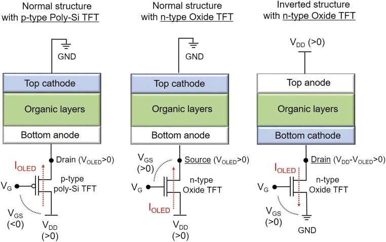
Organic light-emitting diodes (OLEDs) are regarded as next-generation flat-panel displays (4). Although small high-resolution OLED displays are used widely for smart phones/tablets, and large televisions are being commercialized, several issues still remain, such as lifetime, image sticking, power consumption, and production cost (5). The recent high-resolution OLED pixels (6) with reduced aperture ratios [areal ratio of thin-film transistor (TFT) to pixel] raise the importance of the top emission-type structure for practical use. For large OLEDs, it is unrealistic to use low-temperature polycrystalline silicon (LTPS) TFTs for backplanes. Only oxide TFTs, as represented by a-In-Ga-Zn-O (a-IGZO) (7), are practical candidates for the backplane (8, 9). The current small OLEDs use normal-type structures combined with p-channel LTPS TFTs. However, only n-channel TFTs are possible for oxide TFTs in actual applications. Simple substitution of the p-channel LTPS TFTs with n-channel oxide TFTs causes serious problems with stability: Degradation of an OLED pixel and the consequent change in operation voltage directly affect the gate voltage (VGS) of an oxide TFT and alter the current through the OLED pixel, leading to “mura” and image-sticking issues (10), as illustrated in Fig. 1. Using the inverted structure is a straightforward solution to drive OLEDs with the oxide TFT backplane without using pixel compensation circuits (11), but this structure has other challenging issues.
Fig. 1.
Circuits and applied voltages in two types of OLED device structures and driving TFTs with different polarity. Current through OLED (IOLED) is given by IOLED ∝ (VGS – Vth)2 in a saturation region, where VGS and Vth denote the voltage biasing between gate and source and the threshold voltage, respectively. Here VGS = VG – (VDD + VOLED) for n-channel TFTs with normal structure but VGS = VG – VD for p-channel TFTs with normal OLED structure and n-channel TFTs with inverted structure, where VG, VD, and VOLED are gate voltage, drain voltage, and voltage through the OLED, respectively. The variation in the electrical properties of OLED devices, which are sensitive to aging and so on, directly leads to the variation in IOLED, that is, luminous intensity, through the change in VGS. This is why the inverted OLED structure is favorable for being driven by n-channel TFTs with an oxide semiconductor as the active layer.
A major difficulty in fabricating inverted OLEDs with high performance is attributed to the absence of suitable electron-transport/injection materials. The LUMO levels of organic semiconductors are rather high compared with the work functions of conventional metals such as Al (4.1 eV). Thus, an EIL is inserted between a metal cathode and an ETL to reduce the electron injection barrier. Currently, LiF is widely used as the EIL combined with metal Al cathodes (12). Because LiF is a typical wide-gap insulator, a very thin (∼0.5-nm) layer (13) is applied through deposition by vacuum evaporation. The use of this material combination for inverted OLEDs, however, is complicated by the crucial nature of the deposition LiF/Al sequence: When deposition of LiF is followed by the Al layer, the resulting bilayer works well as EIL. However, bilayers fabricated with the inverted sequence (Al →LiF) function poorly (14, 15). This striking difference comes primarily from the reactive nature of the Al atoms created by thermal evaporation. Their reaction with the earlier deposited LiF layer leads to the liberation of Li metal, forming reaction layers with a low work function (13, 14). Thus, the LiF/Al combination does not provide a viable route to OLEDs with an inverted structure.
In terms of alternative systems, alkali/alkaline earth metal or alkali carbonate loadings have been applied to reduce the electron injection barrier, with excellent results (16). Successful attempts to introduce an appropriate interlayer to use surface dipoles (17, 18) have been reported as well. However, applications in commercial products are still limited to the LiF/Al combination, probably because these newer cathode structures have poor chemical stability and/or process incompatibility. Therefore, there is a strong desire for new materials that are process-compatible with intrinsically low work functions and a chemical stability appropriate for practical organic electronic devices.
Another material obstacle in OLEDs is the insufficient performance of the ETL. The ETL has two major roles (19). One is the promotion of smooth electron transfer from the cathode to the emission layer (EML). Second is the suppression of exciton quenching by free carriers in the cathode metal. The current materials used for this purpose are organic n-type semiconductors, represented by tris-(8-hydroxyquinoline) aluminum (Alq3). However, the electron mobility of these organic ETL materials is so small [∼10−6 to ∼10−3 cm2/(V⋅s)] (19) that thick layers create series resistance issues. This restriction imposes several technical challenges such as the inability to effectively eliminate the exciton quenching effect, the frequency of short circuits due to pin hole formation, and the limited range of layer thicknesses that can be used for optimizing light extraction.
Materials Design
Metal oxide thin films are attractive as carrier injection/transport layers (20). In particular, transparent amorphous oxide semiconductors are very favorable due to their process compatibility, chemical stability, optical transparency, and wide tunability of various relevant properties (21). In this work, we designed transparent amorphous oxide semiconductors for EILs and ETLs because these materials form uniform thin films over large areas around room temperature (RT) with high visible transparency. For the ETL, a moderately low work function with an ohmic contact to the cathode is sufficient, but reasonably high electron mobilities are also needed to allow large enough layer thicknesses for the suppression of the exciton quenching effect. For the EIL, the requirement of a very low work function for a low electron injection barrier with an EML is inevitable, but high electron mobility is not needed here because a very thin EIL layer would be sufficient. These materials should be chemically stable and preferably comprise only abundant nontoxic elements that enable low production cost.
For the EIL, we chose a RT-stable amorphous electride. An electride is an ionic compound in which electrons serve as anions (22). Crystalline (c-)12CaO·7Al2O3 electride (C12A7:e−) (23) is a unique conductive oxide with a very small work function (2.4eV) comparable to metal potassium but high chemical inertness (24). These unique properties originate from the intrinsic nature of the anionic electrons accommodated in crystallographic positively charged subnanometer-sized cages. We earlier demonstrated that c-C12A7:e works as a good EIL in OLEDs (25) but the fatal drawback was the high formation temperature of ∼950 °C, which is unrealistic for conventional glass or plastic substrates. In 2011 we reported that a-C12A7:e glass can be obtained by rapid quenching of a c-C12A7:e melt under a low pO2 atmosphere (26). The resulting glass is rather insulating (the RT conductivity is ∼10−8 Scm–1), but to our surprise, despite its amorphous nature it has almost the same anionic electron concentration as c-C12A7:e. This finding implied that a-C12A7:e thin films may be fabricated at RT by conventional sputtering deposition.
Results and Discussion
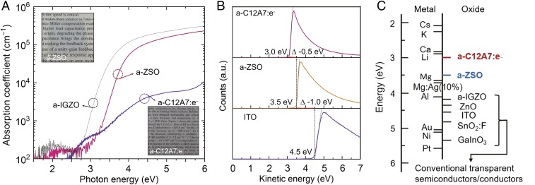
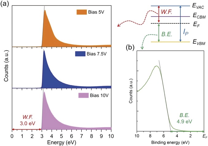
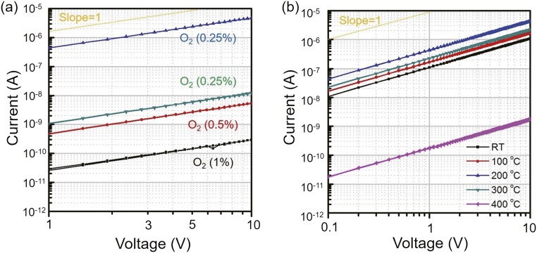
The binary ZnO-SiO2 (ZSO) system was chosen as the ETL material based on its low cost and high visible transparency and the expectation that ZnO would confer a high electron mobility even at amorphous state. SiO2 was selected for two reasons: It facilitates the formation of amorphous ZnO and has a very low electron affinity (∼1 eV), which should lead to a low work function of a-ZSO. Fig. 2A shows the optical absorption spectra of sputter-deposited a-C12A7:e and a-ZSO thin films along with photographs of them. The former has two absorption bands near 3 eV and 4.5 eV, with an absorption tail in the UV region >5eV, but has almost no visible absorption. The optical band gap evaluated from the Tauc plot, (αhv)1/2 vs. hν, was ∼5.3 eV. Electron concentration in the thin film determined by iodometry was ∼0.8 × 1021 cm–1, which is ∼20% less than that of the sintered compact of polycrystalline C12A7:e (∼1 × 1021 cm−3) used as the sputtering target. The a-C12A7:e thin films are almost insulating (conductivity at RT = ∼10−8 Scm−1), in stark contrast with the metallically conductive nature of c-C12A7:e. This result indicates that the free electron concentration in a-C12A7:e is very small. The a-ZSO thin film also has no distinct optical absorption in the visible region, and the Tauc gap of ∼3.5V is slightly larger than that of ZnO (3.3 eV) and a-IGZO (3.2 eV). Fig. 2B and Fig. S1 show the cutoff regions of secondary electron emission from thin films of a-C12A7:e and a-ZSO, with that of an indium tin oxide (ITO) thin film (work function ∼4.5 eV) shown as a reference. The work functions of a-C12A7:e and a-ZSO (0.8ZnO·0.2SiO2) were evaluated to be 3.0 and 3.5 eV, respectively. Table 1 summarizes the physical properties of a-C12A7:e and a-ZSO thin films. The carrier concentration and electron mobility in a-ZSO evaluated by Hall effect measurement are ∼1 cm2/(V⋅s) and ∼1016 cm−3, respectively. This mobility is lower by an order of magnitude than that of polycrystalline ZnO thin films but is higher by six orders of magnitude than that of the conventional organic ETL material Alq3. The carrier concentrations in a-ZSO thin films were reducible to ∼1014 cm–3 by tuning the deposition conditions. Although the work function of a-C12A7:e is larger than that of c-C12A7:e (2.4 eV), this value is still exceptionally low and close to that of metal lithium (2.9 eV). We attribute this low value to the presence of anionic electrons existing at interstitial positions without belonging to specific orbitals of the structure’s ions (27). The work function of a-ZSO (3.5 eV) is significantly lower than that of typical transparent oxide semiconductors (20, 28) including ZnO (4.3eV), as is summarized in Fig. 2C. Note that the work function given above is the minimal value for each material, and the value is adjustable for a-C12A7:e to ∼3.5 eV by reducing the anionic electron concentration, or to ∼4.0 eV for a-ZSO by increasing the SiO2 content from 20 to 25% or control of the partial oxygen pressure during deposition. Even though the work function of a-ZSO (∼3.5 eV) is rather small compared with those of these contact materials (∼4.1 eV for Al and ∼4.5 eV for ITO), good ohmic contacts are formed between them, as shown in Fig. S3. This finding imparts a-ZSO a distinct advantage in its application to ETLs that are directly in contact with the cathode in OLEDs.
Fig. 2.
Physical properties of amorphous C12A7:e and ZSO thin films deposited on SiO2 glass substrates by sputtering at RT. (A) Optical absorption spectra and photographs of the thin films. The sample thicknesses are ∼200 nm. A-ZSO is more transparent than a-IGZO for oxide TFTs. (B) Secondary electron emission cutoff spectra measured by UV photoemission spectroscopy (UPS) along with that of ITO for comparison, and (C) work function values of various metals and transparent oxide semiconductors. Mg:Ag(10%) is practically used as the cathode with a combination of a very thin LiF layer such as LiF/Al (29).
Fig. S1.
UPS spectra of a-C12A7:e thin films. The work function of 3.0 eV was determined from the bias independent secondary electron cutoff (A). The valence band maximum energy was determined to be 4.9 eV from the Fermi level (B). The ionization energy (7.9 eV) is the sum of work function (3.0 eV) and the valence band maximum energy (4.9 eV).
Table 1.
Properties of transparent amorphous oxide semiconductors developed in this work for EILs and ETLs
| Materials | a-C12A7:e | a-ZSO |
| Composition (molar ratio) | Ca:Al:O:e = 24:28:65:2 | 4ZnO-1SiO2 |
| Band gap, eV | ∼5.3 | ∼3.6 |
| Work function, eV | ∼3.0 | ∼3.5 |
| Electron mobility, cm2/(V⋅s) | —* | ∼1 |
| Carrier density, cm−3 | —† | ∼1015 |
| Conductivity at RT, Scm−1 | ∼10−8 | ∼10−4 |
| Electron affinity, eV | ∼2.7 | ∼3.5 |
| Ionization energy, eV‡ | 7.9 | 7.0 |
Fig. S3.
Current–voltage characteristics of the contacts between a cathode metal (Al) and a-ZSO with different resistivities controlled by partial oxygen pressure during deposition (A) or postannealing temperature (B). The resistivity of a-ZSO thin films is adjusted by varying oxygen partial pressure (0.1–1%) during deposition. Ohmic contacts are realized over a wide range of voltages for both metals except an a-ZSO sample with extremely high resistivity that was deposited under the highest PO2 atmosphere.
Fig. S2.
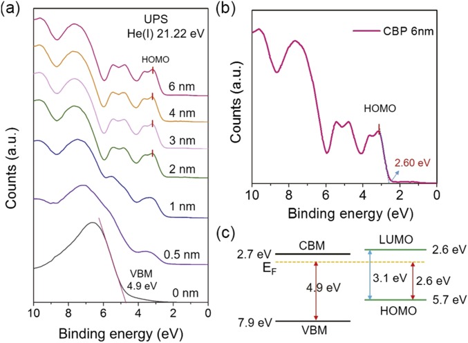
(A) UPS spectra of CBP deposited on a-C12A7:e. (B) Zoomed-in view of the spectrum near the Fermi level. (C) Energy level diagram of a-C12A7:e and CBP. CBM and VBM denote the valence band maximum and conduction band minimum, respectively.
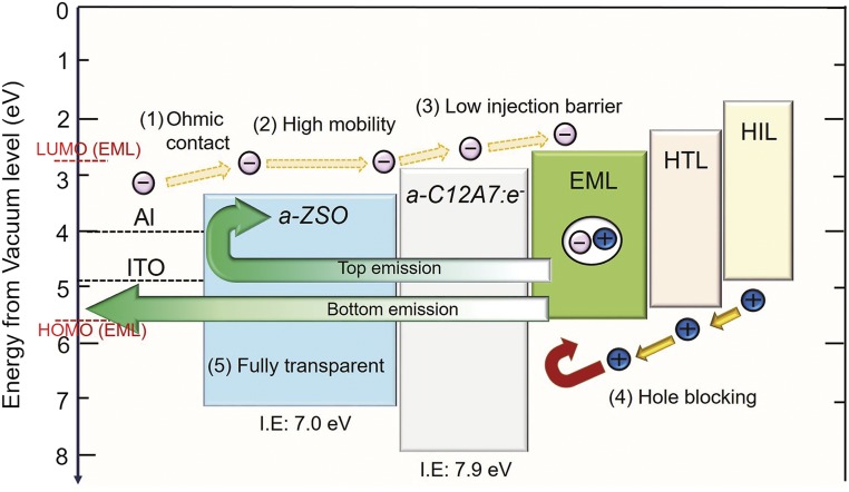
Fig. 3 shows the energy diagram of the inverted OLED using a-ZSO as ETL, a-C12A7:e as EIL, and CBP:Ir(ppy)3 as EML. Smooth electron transport from the cathode to the organic EML can be expected from the small injection barriers between these layers and an ohmic contact between the cathode and the ETL. For hole blocking, a-C12A7:e should work well with its large ionization energy of 7.9 eV (Fig. S1).
Fig. 3.
Energy diagram of an inverted OLED device using a-C12A7:e (EIL) and a-ZSO (ETL). The values of the ionization energy (Ip) were determined from the location of the valence band measured by UPS as shown in Figs. S1 and S2. MoOx and NPD, N,N′-di(1-naphthyl)-N,N′-diphenyl- (1,1′-biphenyl)-4,4′-diamine, are used as hole injection layer (HIL) and HTL, respectively, and CBP doped with Ir(ppy)3, tris[2-phenylpyridinato-C2,N]iridium(III), is used as the EML. Note that the stacking order of injection layer and transport layer for electrons is reversed for the hole. This sequence for the electron is designed to use the ohmic contact between a-ZSO and the cathode materials.
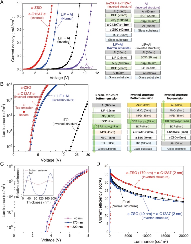
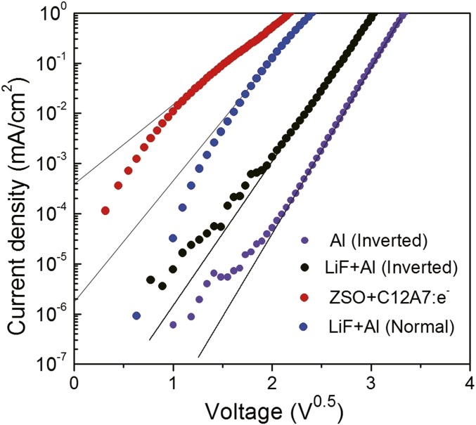
Fig. 4A shows the current–voltage characteristics of electron-only devices with various stacking structures using different EIL and ETL materials. It is evident that the threshold voltage, defined as the voltage for the current reaching 1 mA/cm2, decreases in the order of Al (inverted) = 11.1 V > LiF/Al (inverted) = 9.2 V >> LiF/Al (normal) = 5.7V > a-ZSO/a-C12A7 (inverted) = 4.7 V. The threshold voltage for the inverted device with a-ZSO (ETL, 40 nm)/a-C12A7 (EIL, 4 nm) is much lower than that for the same type of device with Al/LiF (0.5 nm) and is significantly lower than that for the normal type of device with LiF/Al despite the ETL thickness in the former’s being eight times larger than that in the latter. Assuming the difference in current is controlled by the Schottky barrier heights, the difference in the barrier height between the inverted device with a-ZSO/a-C12A7:e and the corresponding devices with LiF/Al or Al is ∼0.3 eV or ∼0.4 eV, respectively (Fig. S4). Fig. 4B compares the luminance performances of inverted and normal-type OLEDs with conventional LiF/Al or a-C12A7:e/a-ZSO/Al (ITO). The threshold voltages of the inverted-type devices with a-C12A7:e/a-ZSO are almost the same or slightly lower than those of the normal-type (conventional) device with LiF/Al. No significant difference was noted between the top and bottom emission types in the former. Fig. 4C shows the a-ZSO layer (ETL) thickness dependence of the luminescent performance of the inverted devices with a-C12A7:e/a-ZSO. The extracted light intensity remains almost unchanged as the a-ZSO thickness is varied from 40 to 320 nm. This result originates from the high mobility and high transparency of a-ZSO and illustrates the distinct advantages of a-ZSO for the ETL. Because the OLED performance is almost independent of the ETL thickness, even over changes by an order of magnitude, one can tune the thickness so as to optimize the light extraction efficiency, as is shown in Fig. 4C, Inset. Fig. 4D shows the relation between current efficiency and luminous intensity for inverted OLEDs and normal OLED with LiF/Al cathode. It is evident that the inverted devices with a-C12A7:e and a-ZSO exhibit current efficiency higher than or almost the same as that of the normal-type device.
Fig. 4.
Comparison of the performance of OLEDs with different stacking structures and different EIL and ETL materials. (A) Current–voltage characteristics of electron-only devices. Alq3 and BCP are used as the electron transport material and hole-blocking material, respectively. (Right) Device stacking structure. (B) Luminous intensity vs. voltage characteristics of OLEDs. (Right) Device stacking structure. (C) The dependence of the luminous characteristics on the ETL thickness. Three thicknesses are chosen to correspond to the calculated optimal values for light extraction from the inverted top emission device. (D) Current efficiency vs. luminance for inverted and normal-type devices. Note that the devices used for this measurement are not the same as those for C but were fabricated by the same procedures as those for C.
Fig. S4.
Log J-V1/2 plots for data on electron-only devices data in Fig. 4A.
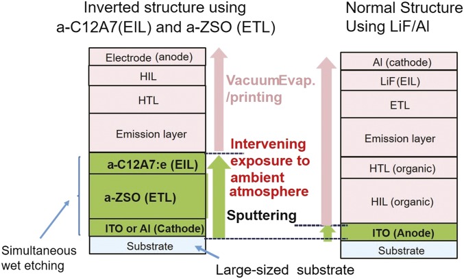
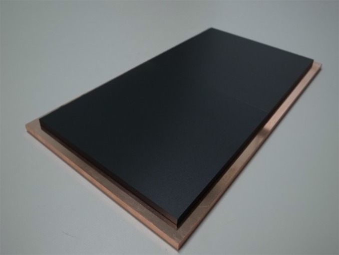
Finally, we would like to address the process advantages of using a-C12A7:e and a-ZSO as reported here in the production of OLEDs. Fig. S5 illustrates the processes proposed here. Both materials have two characteristics as EIL and ETL. Uniform thin films can be deposited over a large area at RT by conventional sputtering (Fig. S6 shows a large-sized C12A7:e ceramic target for sputtering), and the resulting thin films are chemically robust to exposure to the ambient atmosphere. Thus, after the cathode (Al or ITO), ETL (a-ZSO), and EIL (a-C12A7:e) are sequentially deposited on a large substrate with TFT arrays in vacuum, the substrate with its multilayered thin films can be taken out from the vacuum system and transferred for subsequent evaporation or spin-coating processes. When such a transfer entails exposure to the ambient atmosphere, a simple surface cleaning treatment is all that is required. The former processes are practically the same as those in the cost-effective production process of liquid crystal displays. We expect the chemical robustness of these EIL and ETL materials (no electrical and optical degradation was noted for a-ZSO after it was placed for 3 mo in an ambient atmosphere) will enable their use in the conventional production processes of OLEDs. It is anticipated that the transparent amorphous semiconducting oxide materials presented here will enable the fabrication of inverted emission-type OLEDs compatible with oxide TFT backplanes at a reasonable production cost.
Fig. S5.
Proposed process for efficient production of large-sized OLEDs using a-C12A7:e and a-ZSO. The bottom three layers can be deposited by sputtering just as in the practical LCD fabrication process. The resulting multilayer thin films are taken out from the vacuum chamber and then followed by nonvacuum processes used in conventional OLED fabrication shown on the right.
Fig. S6.
Photograph of a sputtering target of c-C12A7:e. The dense sintered targets up to 6 in. in diameter are available.
Materials and Methods
Thin Film Deposition.
Thin films of a-C12A7:e and a-ZSO were deposited on silica glass substrates by rf sputtering with facing targets and offset substrate. Dense sintered compacts of polycrystalline C12A7:e (electron concentration = 1.0 × 1021 cm−3) and 0.8ZnO·0.2SiO2 (in molar ratio) were used as the sputtering targets (Fig. S6). The sputtering gas used was pure Ar (total pressure = 0.1 Pa) for a-C12A7:e or 0.25%O2-Ar (0.4 Pa), and no intentional heating of the substrate during deposition was performed.
The amorphous nature and surface roughness of the resulting thin films were examined by glancing angle X-ray diffraction with a rotating anode source. The work functions of the thin films were evaluated from the cutoff energy for secondary electrons by UPS. Electron concentrations in the a-C12A7:e thin films and the sputtering target were evaluated using the iodometic titration method on solutions of the dissolved materials (26). The electron mobility and carrier concentration of a-ZSO thin films were determined by Hall voltage measurements under an ac magnetic field.
Device Fabrication.
Inverted OLEDs were fabricated as follows. First, a-ZSO and a-C12A7:e layers were sequentially deposited on patterned ITO-deposited silica glass substrates (for bottom emission) or on metal Al-evaporated silica glass substrates using the facing targets sputtering apparatus. Next, each of the resulting substrates was transferred to a vacuum-connected chamber for sequential deposition of organic molecules, MoOx (hole transport layer), and Al (for bottom emission), or a thin Au layer (top emission) by vacuum evaporation without exposure to air.
Acknowledgments
We thank E. Matsuzaki (Tokyo Institute of Technology) and N. Nakamura and N. Miyakawa (Asahi Glass Co. Ltd.) for technical assistance and discussions and D. L. Fredrickson for reading the manuscript. This work was supported in part by funding from the Ministry of Education, Culture, Sports, Science and Technology Element Strategy Initiative to form a research core and Japan Society for the Promotion of Science through a Grant-in-Aid for Research Activity Start-Up, Grant 16H06795 (to J.K.).
Footnotes
The authors declare no conflict of interest.
This article is a PNAS Direct Submission.
This article contains supporting information online at www.pnas.org/lookup/suppl/doi:10.1073/pnas.1617186114/-/DCSupplemental.
References
- 1.Katz HE, Huang J. Thin-film organic electronic devices. Annu Rev Mater Res. 2009;39:71–92. [Google Scholar]
- 2.Gärtner C, et al. The influence of annihilation processes on the threshold current density of organic laser diodes. J Appl Phys. 2007;101(2):023107. [Google Scholar]
- 3.Gong X, et al. Bulk heterojunction solar cells with large open-circuit voltage: Electron transfer with small donor-acceptor energy offset. Adv Mater. 2011;23(20):2272–2277. doi: 10.1002/adma.201003768. [DOI] [PubMed] [Google Scholar]
- 4.Ma R. Organic Electroluminescent Displays. In: Chen J, Cranton W, Fihn M, editors. Handbook of Visual Display Technology. Vol. 2. Springer; Berlin: 2012. pp. 1210–1237. [Google Scholar]
- 5.Chen CW, Lin CL, Wu CC. An effective cathode structure for inverted top-emitting organic light-emitting devices. Appl Phys Lett. 2004;85(13):2469–2471. [Google Scholar]
- 6.Shin HJ, et al. 2015. 7.1: Invited Paper: Novel OLED display technologies for large‐size UHD OLED TVs. SID Symposium Digest of Technical Papers (Wiley, New York), Vol 46, No. 1, pp. 53–56.
- 7.Nomura K, et al. Room-temperature fabrication of transparent flexible thin-film transistors using amorphous oxide semiconductors. Nature. 2004;432(7016):488–492. doi: 10.1038/nature03090. [DOI] [PubMed] [Google Scholar]
- 8.Wager JF. Flat-panel-display backplanes: LTPS or IGZO for AMLCDs or AMOLED displays? Inf Disp. 2014;30(2):26–29. [Google Scholar]
- 9.Arai T. Oxide-TFT technologies for next-generation AMOLED displays. J Soc Inf Disp. 2012;20(3):156–161. [Google Scholar]
- 10.Hsieh HH, et al. Active-matrix organic light-emitting diode displays with indium gallium zinc oxide thin-film transistors and normal, inverted, and transparent organic light-emitting diodes. J Soc Inf Disp. 2011;19(4):323–328. [Google Scholar]
- 11.Han CW, et al. Advanced technologies for UHD curved OLED TV. J Soc Inf Disp. 2015;22(11):552–563. [Google Scholar]
- 12.Hung LS, Tang CW, Mason MG. Enhanced electron injection in organic electroluminescence devices using an Al/LiF electrode. Appl Phys Lett. 1997;70(2):152–154. [Google Scholar]
- 13.Lian JR, et al. LiF thickness dependence of electron injection models for Alq3/LiF/Al cathode structure. Chin Phys Lett. 2014;31(11):118501-1–4. [Google Scholar]
- 14.Heil H, et al. Mechanisms of injection enhancement in organic light-emitting diodes through an Al/LiF electrode. J Appl Phys. 2001;89(1):420–424. [Google Scholar]
- 15.Zhang XW, et al. A very simple method of constructing efficient inverted top-emitting organic light-emitting diode based on Ag/Al bilayer reflective cathode. J Lumin. 2012;132(1):1–5. [Google Scholar]
- 16.Huang J, Xu Z, Yang Y. Low‐work‐function surface formed by solution‐processed and thermally deposited nanoscale layers of cesium carbonate. Adv Funct Mater. 2007;17(12):1966–1973. [Google Scholar]
- 17.Zhou Y, et al. A universal method to produce low-work function electrodes for organic electronics. Science. 2012;336(6079):327–332. doi: 10.1126/science.1218829. [DOI] [PubMed] [Google Scholar]
- 18.Kim YH, et al. Polyethylene imine as an ideal interlayer for highly efficient inverted polymer light-emitting diodes. Adv Funct Mater. 2014;24:3808–3814. [Google Scholar]
- 19.Kulkarni AP, et al. Electron transport materials for organic light-emitting diodes. Chem Mater. 2004;16(23):4556–4573. [Google Scholar]
- 20.Greiner MT, Lu ZH. Thin-film metal oxides in organic semiconductor devices: Their electronic structures, work functions and interfaces. NPG Asia Mater. 2013;5:e55-1-16. [Google Scholar]
- 21.Zhou N, et al. Amorphous oxide alloys as interfacial layers with broadly tunable electronic structures for organic photovoltaic cells. Proc Natl Acad Sci USA. 2015;112(26):7897–7902. doi: 10.1073/pnas.1508578112. [DOI] [PMC free article] [PubMed] [Google Scholar]
- 22.Dye JL. Electrides: Early examples of quantum confinement. Acc Chem Res. 2009;42(10):1564–1572. doi: 10.1021/ar9000857. [DOI] [PubMed] [Google Scholar]
- 23.Matsuishi S, et al. High-density electron anions in a nanoporous single crystal: [Ca24Al28O64]4+(4e-) Science. 2003;301(5633):626–629. doi: 10.1126/science.1083842. [DOI] [PubMed] [Google Scholar]
- 24.Toda Y, et al. Field emission of electron anions clathrated in subnanometer‐sized cages in [Ca24Al28O64]4+(4e–) Adv Mater. 2004;16(8):685–689. [Google Scholar]
- 25.Yanagi H, et al. Low threshold voltage and carrier injection properties of inverted organic light-emitting diodes with [Ca24Al28O64] 4+(4e−) cathode and Cu2−x Se anode. J Phys Chem C. 2009;113(42):18379–18384. [Google Scholar]
- 26.Kim SW, Shimoyama T, Hosono H. Solvated electrons in high-temperature melts and glasses of the room-temperature stable electride [Ca24Al28O64]4+·4e−. Science. 2011;333(6038):71–74. doi: 10.1126/science.1204394. [DOI] [PubMed] [Google Scholar]
- 27.Johnson LE, Sushko PV, Tomota Y, Hosono H. Electron anions and the glass transition temperature. Proc Natl Acad Sci USA. 2016;113(36):10007–10012. doi: 10.1073/pnas.1606891113. [DOI] [PMC free article] [PubMed] [Google Scholar]
- 28.Robertson J, Falabretti B. Electronic structure of transparent conducting oxides. In: Ginley D, Hosono H, Paine DC, editors. Handbook of Transparent Conductors. Springer; Berlin: 2010. pp. 27–50. [Google Scholar]
- 29.Chen B, Sun X, Wong K, Hu X. Enhanced performance of tris-(8-hydroxyquinoline) aluminum-based organic light-emitting devices with LiF/Mg:Ag/Ag cathode. Opt Express. 2005;13(1):26–31. doi: 10.1364/opex.13.000026. [DOI] [PubMed] [Google Scholar]


