Significance
In this work, we investigate the origin of the charge induced in a high-temperature superconducting cuprate film, incorporated in an electric double-layer transistor. Using X-ray spectroscopic measurements made while operating the transistor, together with simulations based on density functional theory, we find that the accumulated charge in the cuprate is due to the depletion of oxygen from specific sites in its unit cell. These results constitute direct evidence of the microscopic mechanism of charge modification. The systematic control of the oxygen content in complex oxides such as the cuprates allows for the study of complex phase diagrams and opens up a route for the design of new complex oxide compounds and devices with improved functionalities.
Keywords: electric double-layer techniques, high-temperature superconductivity, near-edge X-ray absorption spectroscopies, first-principles density functional theory, superconductor-insulator transition
Abstract
Field-effect experiments on cuprates using ionic liquids have enabled the exploration of their rich phase diagrams [Leng X, et al. (2011) Phys Rev Lett 107(2):027001]. Conventional understanding of the electrostatic doping is in terms of modifications of the charge density to screen the electric field generated at the double layer. However, it has been recently reported that the suppression of the metal to insulator transition induced in VO2 by ionic liquid gating is due to oxygen vacancy formation rather than to electrostatic doping [Jeong J, et al. (2013) Science 339(6126):1402–1405]. These results underscore the debate on the true nature, electrostatic vs. electrochemical, of the doping of cuprates with ionic liquids. Here, we address the doping mechanism of the high-temperature superconductor YBa2Cu3O7-X (YBCO) by simultaneous ionic liquid gating and X-ray absorption experiments. Pronounced spectral changes are observed at the Cu K-edge concomitant with the superconductor-to-insulator transition, evidencing modification of the Cu coordination resulting from the deoxygenation of the CuO chains, as confirmed by first-principles density functional theory (DFT) simulations. Beyond providing evidence of the importance of chemical doping in electric double-layer (EDL) gating experiments with superconducting cuprates, our work shows that interfacing correlated oxides with ionic liquids enables a delicate control of oxygen content, paving the way to novel electrochemical concepts in future oxide electronics.
The use of an electric field to modulate the charge density of a material in a controlled way is extensively used in metal oxide semiconductor technology and is also a promising technique to manipulate the properties of complex oxides to generate new devices with exciting functionalities. Many correlated oxides exist in the vicinity of a metal to insulator transition and, as such, their rich phase diagrams are critically controlled by the charge density (1). Gating experiments allowing its controlled modification have attracted much attention (2–8), and in recent years, unprecedented changes in the carrier concentration of complex materials have been achieved by using electric double-layer (EDL) techniques that use ionic liquids (ILs) as gate dielectrics (9–11). Superconductivity has been induced in otherwise band-insulating materials such as SrTiO3 (STO) (12), ZrNCl (13), KTaO3 (14), or MoS2 (15), and the superconducting properties of several cuprates have been tuned to the insulating state (16–20). These results have focused much attention on the EDL technique not only from an applied point of view but also for providing an opportunity to obtain fundamental knowledge about the phase diagrams.
Specifically, in the case of high-temperature cuprate superconductors (16–20), a striking similarity between the bulk phase diagram and the one achieved with the EDL technique was observed. This result demonstrated that the application of positive gate voltages to hole-doped cuprate EDL transistors induces the depletion of charge carriers. Recent results obtained with EDL transistors based on vanadium oxide (VO2) have challenged the conventional interpretation that EDL doping of oxides is due only to the electrostatic screening of the accumulated charges at the interfaces, showing that EDL doping of oxides also involves the migration of oxygen atoms of the crystallographic unit cell (21, 22). These results highlight the necessity of careful studies of the mechanism of doping induced by the electric field generated at the interface between the tested material and the IL to fully understand the innermost origin of the generated electric charge.
Here, we revisit the superconductor to insulator transition of YBa2Cu3O7-X (YBCO) induced by means of the EDL technique while conducting hard X-ray absorption spectroscopy (XAS). We have tuned the cuprate from superconductor to insulator by applying positive gate voltages to an EDL transistor while measuring absorption spectra in the Cu K-edge. Density functional theory (DFT) calculations show that the spectral changes found at the absorption edges arise from oxygen depletion of the CuOx chains. Experiments using intermediate layers acting as oxygen barriers and oxygen reservoirs confirm that the effect of the large electric field at the interface between the IL and the YBCO induces the electromigration of oxygen ions from the CuOx chains. The charge transfer between CuO2 planes and CuOX chains yielding superconducting planes is therefore hindered and the superconductivity suppressed.
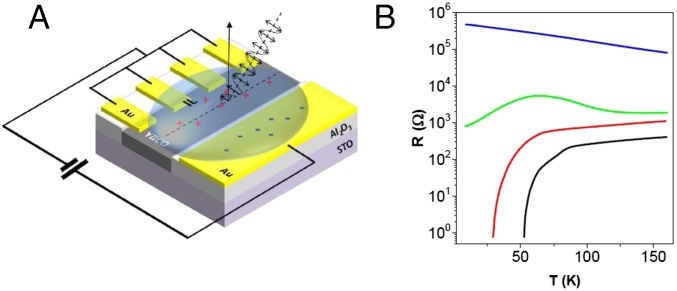
EDL transistors in a side gating geometry (see sketch in Fig. 1A) were fabricated by growing epitaxial YBCO films on prepatterned Al2O3 (ALO) templates prepared on (001)-oriented STO substrates. Fig. 1B shows the resistance–temperature [R(T)] curves corresponding to gate voltages, VG = 0, 4, 5, and 10 V. The fresh sample, without an applied VG, has a TC (superconductor transition temperature) close to the corresponding optimally doped YBCO bulk material and evolves into the insulating state with increasing gate voltage as expected with electron doping (hole depletion).
Fig. 1.
Schematic structure and R(T) measurements of the electric double-layer field-effect transistor using YBCO. (A) Schematic representation of the cuprate electric double-layer transistor device showing the configuration of the gating process and the geometry of the X-ray measurements. (B) Resistance versus temperature curves measured at different gate voltages: 0 V (black), 4 V (red), 5 V (green), and 10 V (blue).
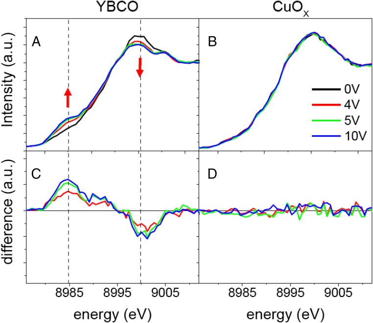
Near-edge X-ray absorption fine structure (NEXAFS) spectra were collected at the Cu K-edge at 10 K simultaneously with gating using an IL. The NEXAFS technique is element-specific, and the spectral features correspond to electronic transitions of the excited core electrons of Cu atoms to unoccupied states. The technique provides local electronic structure and coordination information due to the necessary spatial overlap between the core-level states and the empty final states. In Fig. 2A, we show the NEXAFS spectra collected as a function of the gate voltages 0 V (black line, 4 V (red line), 5 V (green line), and 10 V (blue line). In Fig. 2A, it can be observed that the pre-edge and main edge are both strongly affected by the gating process. Upon positive gating, the intensity of the pre-edge line of the Cu K-edge (labeled A) increases systematically, whereas the intensity of the white line of the resonant peak decreases. In Fig. 2C, we have plotted the difference between the spectra obtained under 4, 5, and 10 V and the spectrum obtained without applied gate voltage (red, green, and blue curves, respectively). The difference is positive around the prepeak of the Cu K-edge, located at ∼8,985 eV, and negative around the main absorption edge, located around 9,000 eV, highlighting the spectral weight transfer between the main edge and the pre-edge that is produced during the gating process.
Fig. 2.
Gate voltage, VG, dependence of Cu K-edge spectra of YBCO. Evolution of the Cu K-edge NEXAFS spectra of YBCO (A) and the CuOX deposited under the gate electrode (B) with increasing gate voltage [0 V (black), 4 V (red), 5 V (green), and 10 V (blue)]. The difference spectra determined by subtracting the 0-V curve from each of the other curves for YBCO and the CuOX are shown in C and D, respectively. As expected the differences for the spectra of the CuOX deposited on top of alumina and under the gold gate electrode are negligible.
As a control test of the experiment, we have measured the Cu K-edge absorption spectra of the binary Cu oxide that grows on top of the alumina and below the gold gate electrode. For these materials, the Cu ions should not be affected by the electric field of the IL that is completely screened at the gold electrode. Fig. 2 B and D exhibits no measurable difference between the spectra measured below the gold electrode at the different applied gate voltages, suggesting that all changes in Fig. 2 A and C arise from the electric field generated at the interface between YBCO and the IL.
In this experiment, we probe core-excited states comprised of a 1s hole and a local electronic p character at the same atomic site consistent with the dipole selection rule. Because NEXAFS is strongly sensitive to hybridization between the Cu and O p orbitals, changes in spectral features can be related to the modification of the local environment around the absorbing species. Aside from this modification, changes in the valence charge of the excited atom modify the core-hole screening and are related to the energy position of the absorbing edge allowing the probe of charge transfer effects.
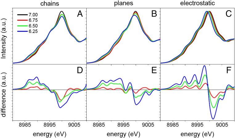
Notably, the changes in the absorption spectra observed when the gate voltage is increased are similar to those found previously (23–27) in NEXAFS spectra of deoxygenated bulk samples, suggesting that oxygen content may be, in fact, modified by doping with the IL. DFT calculations have been used to compute the NEXAFS spectra of several doping scenarios. First, we considered oxygen removal from the CuOx chains corresponding to stoichiometries of YBa2Cu3O7, YBa2Cu3O6.75, YBa2Cu3O6.50, and YBa2Cu3O6.25. In accordance with experimental evidence, we have generated structures with alternating filled and empty chains consistent with each stoichiometry (28). The computed spectra qualitatively reproduce the experimental trends (Fig. 3A).
Fig. 3.
NEXAFS spectra simulations for different oxygen stoichiometries of YBCO. (A) Calculated NEXAFS spectra of YBCO with oxygen stoichiometries corresponding to 7, 6.75, 6.5, and 6.25 (black, red, green, and blue) when the oxygen vacancies are exclusively generated in the CuOX chains. (B) Calculated NEXAFS spectra of YBCO for the same stoichiometries used in A but with the oxygen vacancies generated exclusively in the CuO2 planes. (C) Calculated NEXAFS spectra of YBCO when the compound is electrostatically charged with 0 (7), 0.25 (6.75), 0.5 (6.5), and 0.75 (6.25) electrons per unit cell (corresponding oxygen stoichiometry). D–F show the intensity difference between the calculated spectra for YBCO with oxygen stoichiometries 6.75, 6.5, and 6.25 and the calculated spectra of YBCO with oxygen stoichiometry 7 for the different cases of study. Note that B–F use the same color codes as displayed in A.
Oxygen removal from the CuO2 planes was also considered and ruled out. The simulations shown in Fig. 3B were carried out by removing oxygen from the CuO2 planes up to the same oxygen concentrations considered for the vacancies in the chains. A significant shift of the whole pre-edge region to lower energies is predicted but was not observed in the experimental spectra. The spectral changes are also characterized by a redshift of the white line with decreasing oxygen content, also not found in the experimental data.
Pure electrostatic doping where the YBCO is electron-doped in a fashion similar to that expected for classic field-effect transistors can also be ruled out (Fig. 3C). Different spectra were simulated by adding electrons to match the carrier concentrations corresponding to the oxygen stoichiometries. The resulting spectra exhibit a rigid shift to lower energy due to the increase of the energy of the Fermi level. There are no other changes in the shape, which is at variance with the more complex spectral changes observed in the experimental spectra discussed previously. Only the modification of the pre-edge and main edge computed for oxygen removal from the chains and shown in Fig. 3A are similar to those observed in the gating experiments (Fig. 2B).
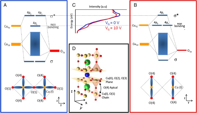
The observed evolution of the spectral features reflects a change in the local electronic structure around the Cu atoms that can be understood using ligand field molecular orbital theory. For YBa2Cu3O7, the pre-edge feature of the K-edge NEXAFS spectrum corresponds to nonbonding 4px states of Cu atoms within the chains. The main edge feature arises from antibonding states between Cu (at the chains 4py and the superconducting planes 4px,y) and 2px,y O atoms. In the absence of vacancies, the 4py orbitals of the Cu atoms in the Cu–O–Cu chains, along the y direction, hybridize with the 2py O states to form occupied sigma bonding, not probed here, and unoccupied σ* antibonding states (Fig. 4A). As O vacancies are created within the chains, the Cu ligand field changes from square planar (Fig. 4A) to linear (Fig. 4B), yielding an intensity increase of the pre-edge feature due to allowed transitions to nonbonding 4py Cu states (Fig. 4C). Spectral weight is thus transferred from the white line to the pre-edge region. The blue and red lines of Fig. 4C represent integrated intensity measured at VG = 0 V and 10 V, respectively, which supports the formation of oxygen vacancies in the Cu chains.
Fig. 4.
Molecular orbitals structure before and after the doping process. Schematic representation of the hybridized molecular orbitals for the two extreme compounds of the YBCO series: YBa2Cu3O7 (A) and YBa2Cu3O6 (B). The Cu coordination in the y-z plane of the CuOX chain structure is also represented. (C) NEXAFS experimental data obtained with a voltage gate of 0 V (blue line) and 10 V (red line) show the spectral weight transfer from the main edge feature to the pre-edge, in agreement with the formation of oxygen vacancies in the Cu chains. (D) YBCO crystallographic structure with the Cu, O, Ba, and Y represented with the yellow, red, green, and blue colors, respectively. The coordination polyhedra of the CuOX chains planes (Top and Bottom) and the superconducting CuO2 planes (Middle) are highlighted as well as the superconducting CuO2 planes. The black arrow illustrates the intraunit cell-charge transfer process between the CuOX chains and the superconducting CuO2 planes.
Therefore, our results are a spectroscopic evidence of chemical changes within the YBCO unit cell (see sketch in Fig. 4D) occurring during the doping process with ILs. The changes in the Cu coordination and consequently in the electronic structure of YBCO indicate oxygen migration under the strong electric field developed at the double layer. Oxygen migration from the CuOx chains is not unrealistic and has been shown to occur in cuprates at moderate temperatures under weak electric fields (29, 30). The strong electric field developing at the double layer is expected to lower the structural barriers for ion motion and generate oxygen vacancies by electromigration.
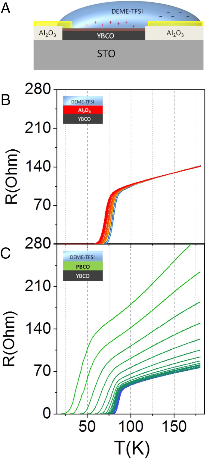
To further verify this scenario, two different gating experiments have been carried out introducing insulating interlayers [either ALO or PrBa2Cu3O7 (PBCO)] between the YBCO and the IL (31). These materials have very different permeability to oxygen ions, which allows for the examination of the role of oxygen out-diffusion from the sample during the doping process. If doping by electrostatics were dominant, we would expect small or no changes in the electric properties of YBCO. ALO and PBCO are both insulating and thus strongly decrease the magnitude of the electric field at the YBCO surface. If doping were the result of the presence of electromigration of oxygen, we would expect a much stronger doping effect in the case of the PBCO interlayer, more permeable to oxygen ions.
In the first case, we have used a 2-nm amorphous ALO interlayer, which acts as a diffusion barrier for oxygen. As shown in Fig. 5A, there is a slight modification of the TC of less than 15 K for gate voltages up to 1.8 V without any alteration of the normal resistance. By further increasing the gate voltages up to 4 V, there is no noticeable changes in the R(T) curves of the ALO/YBCO device. In the second case (Fig. 5B), we have used a two-unit cell PBCO interlayer, isostructural to YBCO, which allows oxygen diffusion into the layer facilitating oxygen migration. Interestingly, in this case, the change of the critical temperature for the same 1.8 V is very pronounced (more than 50 K), in addition there is an increased in the sheet resistance and the measured curves resemble those of deoxygenated YBCO (32). This result confirms that the dominant contribution to the doping of the YBCO using ILs has a chemical origin and arises from the electromigration of oxygen ions from the CuOx chains. Two electrons are supplied by the electrode and thus two holes are annihilated in the YBCO at the interface for every oxygen ion that abandons the YBCO. The present experiment, where the insulating barrier between the YBCO and the IL limits electrostatic doping, constitutes an example of a doping strategy based on oxygen vacancy generation with an IL gate.
Fig. 5.
(A) Schematic structure and R(T) measurements of the electric double-layer field-effect transistor of YBCO with an interlayer. Schematic representation of the gating device showing the configuration with an interlayer between the YBCO and the IL. B and C show resistance versus temperature curves measured at different gate voltages (from 0 V to 1.8 V) when the interlayer is amorphous ALO and isostructural PBCO, respectively. Whereas the amorphous ALO is acting as a physical barrier preventing oxygen diffusion, the PBCO interlayer acts as an oxygen reservoir allowing oxygen migration from the YBCO. C shows a similar behavior of the resistance versus temperature curves of deoxygenated YBCO samples.
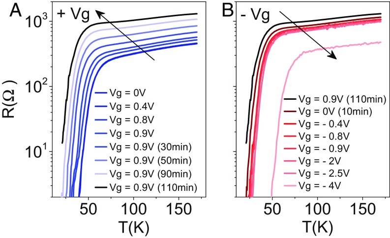
An important issue to address is the reversibility of the doping process. We conducted an experiment (Fig. 6) in which negative voltages were applied to restore the initial state after driving a sample into the underdoped regime by applying positive gate voltages. Notice that here the voltages are smaller than in the gating experiment under the synchrotron beam line of Fig. 1, where the YBCO surface electrode had a larger area by (roughly) a factor of 4 to maximize exposure to the X-ray beam. In this experiment, positive gate voltages were applied in 0.1-V steps up to 0.9 V, which produced a systematic shift of TC. Then, voltage was fixed at this value and we measured the evolution of resistance curves as a function of the polarization time (from 10 to 110 min), which led to further decrease of the critical temperature characteristic of a larger degree of underdoping (Fig. 6A). The decrease of the TC as a function of the polarization time at a constant gate voltage is by itself a strong indication that (apart from the simple electrostatic screening effect) oxygen migration plays a role in the doping process. Afterward, negative gate voltages were applied to restore the initial state. However, larger absolute values of the negative voltages than the positive values necessary to produce the underdoped state were necessary. By applying −4 V, the superconducting critical temperature is fully recovered, showing the reversibility of the gating process. In fact, the TC value for −4 V is even slightly higher than the initial one, which indicates that in addition to oxygen migration an electrostatic effect is present in the doping process (oxygen back-diffusion due to the negative voltages cannot yield larger hole doping than the initial state). Device operation is reversible in so far as the superconductor- insulator transition is not reached, which might result from the difficulty in creating a large homogeneous electric field once the system has reached an insulating state and/or from destructive electrochemical reactions that occur for large oxygen depletion from the sample.
Fig. 6.
Reversibility of the doping process. Resistance versus temperature curves obtained after gating with positive (A) and negative (B) voltages. (A) Positive gate voltages applied in 0.1 V steps up to 0.9 V produce a systematic shift of TC. Fixed gate voltage and increasing polarization time from 10 to 110 min leads to further decrease of the critical temperature underscoring the important oxygen migration role in the doping process. (B) Application of negative gate voltages recovers the initial TC.
We also want to point out that our results are consistent with those of previous studies on IL gating of YBCO samples, where reversible and hysteretic behavior were observed (16, 18), and also with the structural changes after IL gating recently reported in VO2 films (33) (suggesting deoxygenation) and in cuprates (34) (suggesting oxygen displacement rather than deoxygenation), although we go one step further in demonstrating in operando deoxygenation during the gating process by a spectroscopic tool sensitive to oxygen bonding. We note that other electrochemical processes like protonation and hydrogenation have been previously reported for electrolyte-gated VO2 thin films (35, 36). In our case, however, the strong electric field dependence of the effect rules out hydrogenation, which would be driven by neutral hydrogen species. Furthermore, protonation would add free electrons which would reflect in a shift of the white line to lower energies (as we have shown in our DFT simulations), which is not observed experimentally.
In summary, we have provided direct evidence of deoxygenation in IL gating of YBCO. This result outlines the importance of electrochemical processes in doping with ILs. Our work shows the potential of gating with ILs as a powerful tool for the controlled generation of oxygen vacancies in oxides and, thus, signals a path to a new degree of freedom in future oxide electronics devices exploiting phase changes associated to this doping strategy.
Methods
EDL Transistors.
EDL transistors were fabricated on top of (001)-oriented STO substrates using a pattern of nanocrystalline ALO that allowed us to define the active channel of the YBCO (gray rectangle in Fig. 1A) as well as the gold electrodes for the transport measurements and the gating process (top yellow rectangles and the bottom yellow rectangle of the sketch in Fig. 1A), respectively. The three-unit-cell-thick YBCO thin film was grown on top of a five-unit-cell-thick PBCO buffer layer to ensure optimal superconducting properties (37). Both layers, which had excellent epitaxial properties, were grown using a high-pressure pure oxygen-sputtering system at a substrate temperature of 900 °C. Notice that on top of the bare STO substrate, the films are epitaxial, whereas on top of the nanocrystalline ALO, there is no growth of YBCO and PBCO, but there is the deposition of mixed binary oxides. The gate dielectric was formed by depositing a 1-μL drop of the IL DEME-TFSI, as sketched in Fig. 1A. To prevent the reaction of the surface of the sample with water in the IL, the N,N-diethyl-N-(2-methoxyethyl)-N-methylammonium bis(trifluoromethylsulphonyl)imide (DEME-TFSI) was baked at 100 °C and at 10−2 torr for a period of 24 h. The IL drop was held on top of the device and spread over the surface of the sample using a 10-μm-thick polyester film, which allowed for a vertical orientation of the substrate inside the He flow cryostat in the synchrotron experiment. Notice that in the synchrotron configuration the YBCO surface electrode had a larger area than in the reversibility experiment of Fig. 6 by (roughly) a factor of 4 to maximize exposure to the X-ray beam.
X-Ray Absorption Experiments.
NEXAFS spectra were collected at the Cu K-edge at 10 K at the Beamline BM25A of the European Synchrotron Radiation Facility. The synchrotron measurements were done with linearly polarized X-rays with an incident angle of 40° with respect to the normal of the sample (Fig. 1A). The XAS signal was collected with a fluorescence detector mounted at an angle of 10° with respect to the normal of the sample surface. The gate voltage (VG) was applied at 220 K for a period of 10 min, and the device was immediately cooled down to 10 K. Due to the complex set up in the XAS line and the dependence of the gate voltages on the polarization temperature, it was necessary to apply high VG to have standard values of the leakage current in the charging process. The R(T) curves were recorded during the warming of the sample up to 180 K, and the XAS measurements were done at 10 K.
DFT Calculations.
We simulated the X-ray absorption spectra using a plane-wave pseudopotential orbital occupancy-constrained DFT framework, using the Perdew–Burke–Ernzerhof functional within the plane-wave self-consistent field package (38). For each configuration, we optimized both atomic positions and lattice parameters. The transition amplitudes were calculated according to Fermi’s golden rule for the absorption cross-section within the electric-dipole approximation. We also computed the quadrupole matrix elements and found that they contribute negligibly to the total transition amplitudes. The initial and final states were single-particle Kohn–Sham eigenstates of the ground and excited-state self-consistent field, respectively. The initial state was the 1s orbital of Cu and the final state were accessible Kohn–Sham eigenstates derived from a self-consistent field computed within the excited electron and core-hole approximation. Two similar implementations were used to compute the spectra yielding the same result, the xspectra utility (39) and the method by Prendergast et al. (40, 41). Starting from the transition amplitudes, the final spectra were computed using a Gaussian convolution of 0.8 eV using the experimental direction of the X-ray polarization. An average in-plane polarization was considered to mimic the presence of domains in the experiment.
Acknowledgments
R.P. acknowledges D. Prendergast for discussions. The authors acknowledge the Spanish Collaborating Research Group Beamline (SpLine) staff for their valuable help. A.M.G. was supported partially by US National Science Foundation Award DMR-1420013 through the Minnesota Materials Research Science and Engineering Center and by US National Science Foundation Award DMR-1209578. J.G.-B. acknowledges support from the Ministerio de Economía, Industria y Competitividad (MINECO) through the Ramon y Cajal Program and through MINECO Award PCIN-2013-061. Calculations were performed using computer resources from Genci Grand Équipement National de Calcul Intensif under Centre Informatique National de l’Enseignement Suprieur Grants c2015097211 and c2016097211. Work at Universidad Complutense de Madrid was supported by the Spanish MINECO through Grants MAT2014-52405-C02-01 and Consolider Ingenio 2010-CSD2009-00013 (Imagine) and by Comunidad Autonoma de Madrid (CAM) through Grant CAM S2013/MIT-2740. The SpLine beamline is supported financially by the Spanish MINECO and Consejo Superior de Investigaciones Cientificas under Grant PIE 2010 6 OE 013. P.S. acknowledges the support from Fundação de Amparo à Pesquisa do Estado de São Paulo Projects 2012/18397-2 and 2013/12537-9.
Footnotes
The authors declare no conflict of interest.
This article is a PNAS Direct Submission. I.B. is a Guest Editor invited by the Editorial Board.
References
- 1.Imada M, Fujimori A, Tokura Y. Metal-insulator transitions. Rev Mod Phys. 1998;70:1039–1263. [Google Scholar]
- 2.Ahn CH, Triscone JM, Mannhart J. Electric field effect in correlated oxide systems. Nature. 2003;424(6952):1015–1018. doi: 10.1038/nature01878. [DOI] [PubMed] [Google Scholar]
- 3.Ahn CH, et al. Electrostatic modification of novel materials. Rev Mod Phys. 2006;78:1185–1212. [Google Scholar]
- 4.Mannhart J, Schlom DG. Oxide interfaces--an opportunity for electronics. Science. 2010;327(5973):1607–1611. doi: 10.1126/science.1181862. [DOI] [PubMed] [Google Scholar]
- 5.Cassinese A, De Luca GM, Prigiobbo A, Salluzzo M, Vaglio R. Field-effect tuning of carrier density in Nd1.2Ba1.8Cu3Oy thin films. Appl Phys Lett. 2004;84:3933–3935. [Google Scholar]
- 6.Salluzzo M, et al. Indirect electric field doping of the CuO2 planes of the cuprate NdBa2Cu3O7 superconductor. Phys Rev Lett. 2008;100(5):056810. doi: 10.1103/PhysRevLett.100.056810. [DOI] [PubMed] [Google Scholar]
- 7.Parendo KA, et al. Electrostatic tuning of the superconductor-insulator transition in two dimensions. Phys Rev Lett. 2005;94(19):197004. doi: 10.1103/PhysRevLett.94.197004. [DOI] [PubMed] [Google Scholar]
- 8.Ueno K, et al. Field-effect transistor on SrTiO3 with sputtered Al2O3 gate insulator. Appl Phys Lett. 2003;83:1755–1757. [Google Scholar]
- 9.Shimotani H, et al. Insulator to metal transition in ZnO by electric double layer gating. Appl Phys Lett. 2007;91:15–18. [Google Scholar]
- 10.Yuan H, et al. High-density carrier accumulation in ZnO field-effect transistors gated by electric double layers of ionic liquids. Adv Funct Mater. 2009;19:1046–1053. [Google Scholar]
- 11.Yamada Y, et al. Electrically induced ferromagnetism at room temperature in cobalt-doped titanium dioxide. Science. 2011;332(6033):1065–1067. doi: 10.1126/science.1202152. [DOI] [PubMed] [Google Scholar]
- 12.Ueno K, et al. Electric-field-induced superconductivity in an insulator. Nat Mater. 2008;7(11):855–858. doi: 10.1038/nmat2298. [DOI] [PubMed] [Google Scholar]
- 13.Ye JT, et al. Liquid-gated interface superconductivity on an atomically flat film. Nat Mater. 2010;9(2):125–128. doi: 10.1038/nmat2587. [DOI] [PubMed] [Google Scholar]
- 14.Ueno K, et al. Discovery of superconductivity in KTaO3 by electrostatic carrier doping. Nat Nanotechnol. 2011;6(7):408–412. doi: 10.1038/nnano.2011.78. [DOI] [PubMed] [Google Scholar]
- 15.Ye JT, et al. Superconducting dome in a gate-tuned band insulator. Science. 2012;338(6111):1193–1196. doi: 10.1126/science.1228006. [DOI] [PubMed] [Google Scholar]
- 16.Leng X, Garcia-Barriocanal J, Bose S, Lee Y, Goldman AM. Electrostatic control of the evolution from a superconducting phase to an insulating phase in ultrathin YBa2Cu3O(7-x) films. Phys Rev Lett. 2011;107(2):027001. doi: 10.1103/PhysRevLett.107.027001. [DOI] [PubMed] [Google Scholar]
- 17.Bollinger AT, et al. Superconductor-insulator transition in La2c - cxSrxCuO4 at the pair quantum resistance. Nature. 2011;472(7344):458–460. doi: 10.1038/nature09998. [DOI] [PubMed] [Google Scholar]
- 18.Leng X, et al. Indications of an electronic phase transition in two-dimensional superconducting YBa2Cu3O(7-x) thin films induced by electrostatic doping. Phys Rev Lett. 2012;108(6):067004. doi: 10.1103/PhysRevLett.108.067004. [DOI] [PubMed] [Google Scholar]
- 19.Garcia-Barriocanal J, et al. Electronically driven superconductor-insulator transition in electrostatically doped La2CuO4+δ thin films. Phys Rev B. 2013;87:1–11. [Google Scholar]
- 20.Zeng SW, et al. Two-dimensional superconductor-insulator quantum phase transitions in an electron-doped cuprate. Phys Rev B. 2015;92:020503. [Google Scholar]
- 21.Li M, et al. Suppression of ionic liquid gate-induced metallization of SrTiO3(001) by oxygen. Nano Lett. 2013;13(10):4675–4678. doi: 10.1021/nl402088f. [DOI] [PubMed] [Google Scholar]
- 22.Jeong J, et al. Suppression of metal-insulator transition in VO2 by electric field-induced oxygen vacancy formation. Science. 2013;339(6126):1402–1405. doi: 10.1126/science.1230512. [DOI] [PubMed] [Google Scholar]
- 23.Gaur A, Shrivastava BD, Joshi SK. Copper K-edge XANES of Cu(I) and Cu(II) oxide mixtures. J Phys Conf Ser. 2009;190:012084. [Google Scholar]
- 24.Tolentino H, et al. Valence changes of copper under oxygen uptake and removal in YBa2Cu3O7−δ observed in situ by X-ray absorption spectroscopy. Phys Lett A. 1989;139:474–480. [Google Scholar]
- 25.Tranquada JM, Heald SM, Moodenbaugh AR, Xu Y. Mixed valency, hole concentration, and Tc in YBa2Cu. Phys Rev B Condens Matter. 1988;38(13):8893–8899. doi: 10.1103/physrevb.38.8893. [DOI] [PubMed] [Google Scholar]
- 26.Lwazumi T, et al. Study on copper valency of high Tc superconductor YBa2Cu3O7−δ by high temperature X-Ray Absorption Spectroscopy. Solid State Commun. 1988;65(3):213–217. [Google Scholar]
- 27.Gauquelin N, et al. Atomic scale real-space mapping of holes in YBa2Cu3O(6+δ) Nat Commun. 2014;5:4275. doi: 10.1038/ncomms5275. [DOI] [PubMed] [Google Scholar]
- 28.Hawthorn DG, et al. Resonant elastic soft X-Ray scattering in oxygen-ordered YBa2Cu3O6+x. Phys Rev B. 2011;84:075125. [Google Scholar]
- 29.Moeckly BH, Lathrop DK, Buhrman RA. Electromigration study of oxygen disorder and grain-boundary effects in YBa2Cu3O7- δ thin films. Phys Rev B. 1990;47:400–417. doi: 10.1103/physrevb.47.400. [DOI] [PubMed] [Google Scholar]
- 30.Govinda Rajan K, Parameswaran P, Janaki J, Radhakrishnan TS. Electromigration of oxygen in YBa2Cu3O7- δ. J Phys D Appl Phys. 1993;23:694–697. [Google Scholar]
- 31.Zhou Y, et al. Control of emergent properties at a correlated oxide interface with graphene. Nano Lett. 2015;15(3):1627–1634. doi: 10.1021/nl504170d. [DOI] [PubMed] [Google Scholar]
- 32.Sefrioui Z, et al. Crossover from a three-dimensional to purely two-dimensional vortex-glass transition in deoxygenated YBa2Cu3O7-x thin films. Phys Rev B. 1999;60:423–429. [Google Scholar]
- 33.Jeong J, et al. Giant reversible, facet-dependent, structural changes in a correlated-electron insulator induced by ionic liquid gating. Proc Natl Acad Sci USA. 2015;112(4):1013–1018. doi: 10.1073/pnas.1419051112. [DOI] [PMC free article] [PubMed] [Google Scholar]
- 34.Dubuis G, et al. Oxygen displacement in cuprates under ionic liquid field-effect gating. Sci Rep. 2016;6:32378. doi: 10.1038/srep32378. [DOI] [PMC free article] [PubMed] [Google Scholar]
- 35.Ji H, Wei J, Natelson D. Modulation of the electrical properties of VO2 nanobeams using an ionic liquid as a gating medium. Nano Lett. 2012;12(6):2988–2992. doi: 10.1021/nl300741h. [DOI] [PubMed] [Google Scholar]
- 36.Shibuya K, Sawa A. Electrolyte gating on oxygen-deficient VO2 thin films. Adv Electron Mater. 2016;2:1500131. [Google Scholar]
- 37.Varela AM, et al. Effects of epitaxial strain on the growth mechanism in YBa2Cu3O7-x thin films in YBa2Cu3O7-x / PrBa2Cu3O7 superlattices. Phys Rev B. 2002;66:174514. [Google Scholar]
- 38.Giannozzi P, et al. QUANTUM ESPRESSO: a modular and open-source software project for quantum simulations of materials. J Phys Condens Matter. 2009;21(39):395502. doi: 10.1088/0953-8984/21/39/395502. [DOI] [PubMed] [Google Scholar]
- 39.Gougoussis C, Calandra M, Seitsonen AP, Mauri F. First-principles calculations of X- ray absorption in a scheme based on ultrasoft pseudopotentials: From α-quartz to high-Tc compounds. Phys Rev B. 2009;80:075102. [Google Scholar]
- 40.Prendergast D, Galli G. X-ray absorption spectra of water from first principles calculations. Phys Rev Lett. 2006;96(21):215502. doi: 10.1103/PhysRevLett.96.215502. [DOI] [PubMed] [Google Scholar]
- 41.Prendergast D, Louie SG. Bloch-state-based interpolation: An efficient generalization of the Shirley approach to interpolating electronic structure. Phys Rev B. 2009;80:235126. [Google Scholar]


