Significance
In this article, we use microscopic rhombic dodecahedra made from DNA-programmable assembly of programmable atom equivalents (i.e., DNA-functionalized nanoparticles), to study the importance of nano- and microscopic architecture on directional light emission. The DNA sequence design provides subnanometer control over the interactions between light-emitting molecules and metal nanoparticles, resulting in micrometer-scale light–matter interactions which induce unique spatial and spectral emission profiles. Electrodynamics calculations combining the two scales successfully model the observed behaviors. This initial study provides a compelling demonstration of the utility of DNA-programmable assembly for making 3D photonic devices that uniquely allow one to engage in structure–function relationship studies, important in fields spanning quantum electrodynamics and plasmonics.
Keywords: DNA programmable assembly, directional emission, anisotropic 3D microcavity, nanoparticle surface plasmon, fluorescence enhancement
Abstract
Three-dimensional plasmonic superlattice microcavities, made from programmable atom equivalents comprising gold nanoparticles functionalized with DNA, are used as a testbed to study directional light emission. DNA-guided nanoparticle colloidal crystallization allows for the formation of micrometer-scale single-crystal body-centered cubic gold nanoparticle superlattices, with dye molecules coupled to the DNA strands that link the particles together, in the form of a rhombic dodecahedron. Encapsulation in silica allows one to create robust architectures with the plasmonically active particles and dye molecules fixed in space. At the micrometer scale, the anisotropic rhombic dodecahedron crystal habit couples with photonic modes to give directional light emission. At the nanoscale, the interaction between the dye dipoles and surface plasmons can be finely tuned by coupling the dye molecules to specific sites of the DNA particle-linker strands, thereby modulating dye–nanoparticle distance (three different positions are studied). The ability to control dye position with subnanometer precision allows one to systematically tune plasmon–excition interaction strength and decay lifetime, the results of which have been supported by electrodynamics calculations that span length scales from nanometers to micrometers. The unique ability to control surface plasmon/exciton interactions within such superlattice microcavities will catalyze studies involving quantum optics, plasmon laser physics, strong coupling, and nonlinear phenomena.
Microcavities are important photonic architectures that can be used to couple dipole emitters with optical modes and enhance light–matter interactions typically with long cavity lifetimes (high Q factors). They have been used to understand phenomena in cavity quantum electrodynamics (1, 2), and to enable molecular sensing (3) and lasing (4) technologies. In recent years, researchers have developed strategies for incorporating plasmonic nanostructures into microcavity structures to enhance light–matter interactions via strong light confinement (small mode volume, V), resulting in materials that are capable of plasmon lasing (5–7). These plasmonic microcavities exploit two different aspects of the architectures simultaneously: guided optical modes that resonate or scatter light (via the microcavity geometry) and near-field–driven optical confinement (via the metallic nanostructure). Such hybrid photonic structures are desirable because they can lead to high Q factors and strong light confinement within a single architecture, significantly enhancing light–matter interactions by a large cavity figure of merit, Q/V. However, most of the plasmonic microcavities have been limited to 1D or 2D microcavity geometries and plasmonic mode confinement (7) (metallic nanostructures) due to limitations in fabrication methods (6, 8). Importantly, 3D counterparts of these 1D and 2D architectures can lead to interesting properties such as higher microcavity Q factors (2), 3D angular emission dependence, and stronger mode confinement (7).
DNA-guided nanoparticle colloidal crystallization provides remarkable control over the assembly of nanoparticles into superlattices (9, 10), enabling the deliberate tailoring of crystal symmetry (9), lattice constant (11), and particle composition (12). Furthermore, structures with geometrically well-defined 3D crystal habits (10), when locked into the solid state via silica embedding procedures (13), open up potential applications in the field of optics. Therefore, these methods provide exciting possibilities for controlling the interaction between photonic modes of microcavity structures and plasmonic modes of the highly polarizable nanoparticles for nano-/micrometer-scale optical applications. Indeed, it was recently demonstrated that one can control the strength of coupling between Fabry–Perot modes and localized surface plasmons in a body-centered cubic (bcc) crystal composed of gold nanoparticles with a rhombic dodecahedron (RD) crystal habit (14). Such superstructures behave as 3D plasmonic microcavities (passive cavities) that exhibit both guided modes and plasmonic near-field effects throughout the cavity medium. Therefore, upon incorporating excitonic materials into these superlattices, the nature of such 3D plasmonic microcavities (active cavities) can be explored systematically through an analysis of excitonic emission properties.
In this work, we synthesize dye-functionalized plasmonic superlattices via DNA programmable assembly (10, 14), and study their emission properties both experimentally and theoretically. The plasmonic microcavity emission behavior of these crystals is first investigated via a spatio-spectral analysis, and the ability to control the interaction between plasmonic nanoparticles and dye excitons via dye placement within the structure is studied by decay lifetime measurements.
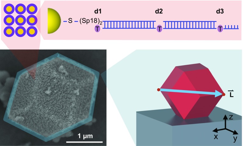
To construct a dye-functionalized plasmonic microcavity, bcc superlattices with a 52-nm lattice constant were synthesized from DNA-functionalized 20-nm-diameter gold nanoparticles (Fig. 1; Dye-Coupled Plasmonic Superlattice Microcavity Fabrication, Dye-Labeled DNA Synthesis and Dye-Coupled Plasmonic Superlattice Microcavity Fabrication, DNA Nanoparticle Conjugate Preparation). Such structures have a gold volume fraction (FF) of about 6%. A scanning electron microscope (SEM) image confirms the micrometer size of the crystals and the well-defined RD crystal habit (Fig. 1, Bottom). To describe the crystal orientations in this work, is defined as the vector connecting two vertices with the largest intervertex distance (Fig. 1, Bottom Right). The RD crystal habit can induce anisotropic microcavity properties (15) due to its geometry. Specifically, light emitted from the dye–Au nanoparticle complexes (lattice sites) can be scattered by the RD architecture leading to an angular dependence of the cavity emission profile in 3D. Simultaneously, due to internal reflection at facets of the RD habit, optical resonant modes can be established based on its intrinsic symmetry as in the case of its spherical counterpart (2, 3). Overall, these microcavity properties can be influenced by the plasmonic resonance of the nanoparticle lattice that modulates real and imaginary parts of the microcavity refractive index (14). To incorporate dye excitons at the nanoscale, DNA strands were synthesized with amino-modified dT bases where dye-labeled NHS esters can bind (Fig. 1, Top and Table S1). Specifically, to control the interaction between the dye excitons and plasmonic nanoparticles (16, 17), three dye-to-gold surface distances (1, 5, and 11 nm; denoted d1, d2, and d3, respectively) were used. In addition, Alexa Fluor 532 and 700 dyes were used to study the importance of spectral overlap between the dye (exciton) emission and the frequency of the localized surface plasmon resonance (LSPR; ∼520 nm). Approximately 120 dye molecules were attached to each gold nanoparticle, as determined by fluorophore assays (Supporting Information). Due to the small size of the nanoparticles, lattice sites can be considered dipole emitters. The loading of fluorophores on our nanoparticles could give lower dye quantum yields and altered dye lifetimes due to energy transfer (17), but the low particle density is such that this should not influence the emission angular profile (and our modeling confirms this).
Fig. 1.
Scheme showing the 3D microcavity geometry (blue, Bottom Right) and a dye-coupled gold nanoparticle (magenta, Top) of dye-functionalized single-crystal bcc superlattices. An SEM image shows a representative superlattice (Bottom Left). The superlattice is drop-cast onto a glass substrate leading to a facet facing up orientation (Bottom Right). Its RD shape can lead to 3D microcavity properties. is defined as a vector connecting two vertices (two red dots) with the largest intervertex distance (blue arrow aligned with y axis, Bottom Right). Three s can be defined in an RD, and they all pass through the center of the structure. The gold nanoparticles at the lattice sites in the superlattice (Top) are surrounded by multiple dye molecules forming a layer, and the distance between the gold surface and the dye layer is controlled by selecting a dye binding site among three sites (purple circles; denoted d1, d2, and d3 from left to right) on DNA strands (Dye-Coupled Plasmonic Superlattice Microcavity Fabrication, Dye-Labeled DNA Synthesis; and Dye-Coupled Plasmonic Superlattice Microcavity Fabrication, DNA Nanoparticle Conjugate Preparation). The dye molecules are chosen based on the spectral positions of their emission with respect to that of the surface plasmons, depending on the intended use.
Table S1.
DNA sequences used in this work
| Strand | Description | Sequence |
| Thiolated strands | ||
| 1 | AuNP-bound strand | 5′TCC ACT CAT ACT CAG CAA (Spacer18*)2 SH 3′ |
| 2 | AuNP-bound strand | 5′TCA ACT ATT CCT ACC TAC (Spacer18)2 SH 3′ |
| Linker strands | ||
| 3 | d1 linker for 1 | 5′(A-dT†) TTG CTG AGT ATG AGT GGA TTT ACT GAG CAG CAC TGA TTT T AAGGAAA 3′ |
| 4 | d1 linker for 2 | 5′(A-dT) GTA GGT AGG AAT AGT TGA TTT ACT GAG CAG CAC TGA TTT T TTTCCTT 3′ |
| 5 | d2 linker for 1 | 5′T TTG CTG AGT ATG AGT GGA (A-dT) TT ACT GAG CAG CAC TGA TTT T AAGGAAA 3′ |
| 6 | d2 linker for 2 | 5′T GTA GGT AGG AAT AGT TGA (A-dT) TT ACT GAG CAG CAC TGA TTT T TTTCCTT 3′ |
| 7 | d3 linker for 1 | 5′T TTG CTG AGT ATG AGT GGA TTT ACT GAG CAG CAC TGA TTT (A-dT) AAGGAAA 3′ |
| 8 | d3 linker for 2 | 5′T GTA GGT AGG AAT AGT TGA TTT ACT GAG CAG CAC TGA TTT (A-dT) TTTCCTT 3′ |
| 9 | Duplexer | 5′AAT GAC TCG TCG TGA CTA AA 3′ |
“Spacer18” refers to the Spacer Phosphoramidite 18 manufactured by Glen Research.
“A-dT” refers to Amino-Modifier C6 dT manufactured by Glen Research.
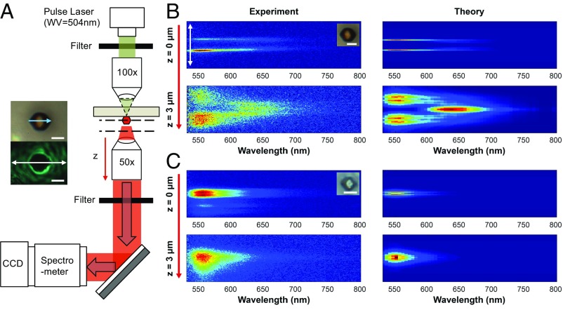
The plasmonic microcavity behavior of the silica encapsulated superlattices was probed with a pulsed laser coupled microspectrophotometry system (Fig. 2A and Fig. S1). A d1 superlattice with Alexa Fluor 532 dyes was chosen to determine the effect of superlattice microstructure on directional emission. Spatio-spectral emission data were collected from 515 to 800 nm to include the LSPR frequency to understand the surface plasmon contributions to emission behavior. A 50-µm slit was used to collect light from a thin line cutting through the superlattice center (Fig. 2A, white arrow) and also to provide spectral resolution. In the collection process, the long axes of the superlattices (Fig. 2A, blue arrow; in Fig. 1, Right) were aligned with the slit to analyze the emitted light from an angle parallel to . The spatio-spectral emission profile of the superlattice with L∼5 µm (Fig. 2B, Left) shows a transition from a double-line shape to a triangular shape as the focal plane of the objective lens is moved away from the center of the superlattice (red arrows in Fig. 2 A and B). Such profiles (Fig. 2B, Left) are observed from single-crystal superlattices with well-formed RD crystal habits, whereas polycrystalline superlattices of random micrometer-scale shapes do not show such profiles (Fig. S2). To understand the effect of plasmonic nanoparticles in the microcavity, the same analysis was performed with a gold-etched control (and therefore gold-free) d1 superlattice (dielectric RD structure; Fig. 2C, Inset). Its spatio-spectral profile (Fig. 2C) does not exhibit the profile exhibited by its plasmonic counterpart (Fig. 2B, Left), and its emission spectral range is narrow (λ ∼ 550–650 nm), similar to that of Alexa Fluor 532 free dye dissolved in water (Theoretical Analysis of Superlattice Microcavity Emission Behavior, Quantum Yield [q(λ)] and Enhanced Decay Rates of a Dye Around a Gold Nanoparticle; Fitting of the Theoretical Spatio-Spectral Emission Profile []). These experiments demonstrate the strong near-field contributions of the plasmonic nanoparticles to the emission profile of the superlattice. Specifically, strong mode confinement and absorption (Fig. 2B) broaden and modify the spectral profile of exciton emission (7).
Fig. 2.
Spatio-spectral analysis of microcavity dye emission. (A) Optical experiment setup for spatio-spectral analysis. Laser pulses (λ = 504 nm, pulse width ∼100 ps, spot size of ∼5–10 µm) were used in transmission mode and focused through a 100× objective lens to excite a single superlattice. The superlattice emission was collected with a 50× objective lens and spatio-spectral analysis was collected via a spectrometer and a CCD. Two filter sets, band-pass and long-pass, were used to narrow the pulsed laser linewidth and to reject part of the laser light. The focal plane of the 50× objective lens was tuned to generate data at multiple focal planes (dashed lines). The orientation of the superlattice and substrate are reversed from that depicted in Fig. 1 (Bottom Right), as their z axes indicate. Optical images show a bright-field image of a superlattice on a glass substrate with denoted (blue arrow, Top) and the same superlattice illuminated by the pulse laser (Bottom). The white arrow indicates the slit location. (B) Spatio-spectral emission profile (Left) of a d1 superlattice (L ∼ 5 µm, Inset) compared with the theoretical prediction (Right). The top images were formed with the focal plane located around the center of the superlattice and the bottom with the focal plane 3 µm below it (see the scheme in A). Emitted light was collected with a slit cutting through the center of the superlattice (white arrow in A) where spatial (vertical axis of the profile, 30 µm) and spectral information were collected (horizontal axis of the profile). (C) Comparable data for a gold-etched control d1 superlattice were investigated to analyze the effect of plasmonic absorbers. The gold-etched control superlattice is transparent due to lack of nanoparticle absorption (Inset). (Scale bar, 5 µm.)
Fig. S1.
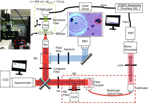
Scheme of the optical setup used to measure spatio-spectral superlattice emission and dye decay lifetimes. Spatio-spectral analysis is performed with a CCD and a spectrometer (left on the scheme). Lifetime measurements were performed with a photomultiplier tube (PMT) and TCSPC electronics (right on the scheme). Two light sources were used: a xenon lamp (XBO) for imaging and a pulse laser for superlattice excitation. The green and red dashed boxes in the scheme and the image (Left) show an optomechanical pulse laser coupling system and a fiber coupling system, respectively.
Fig. S2.
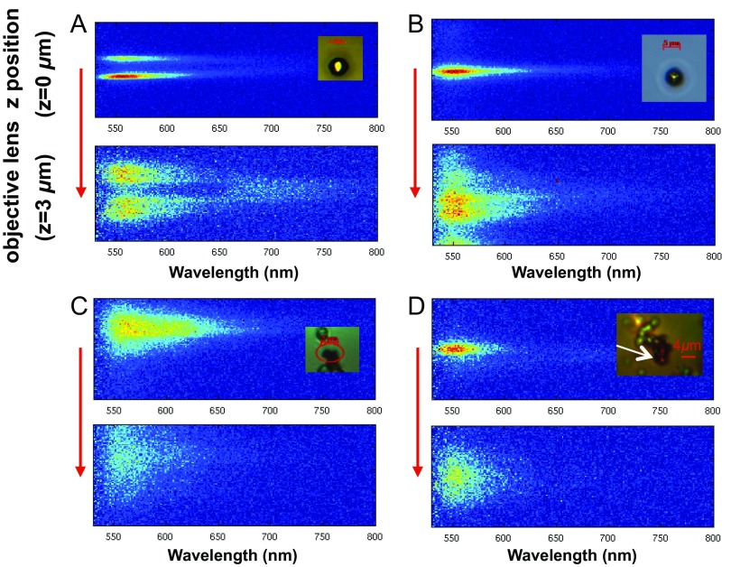
Spatio-spectral emission profiles of various control samples. d2 superlattice (A), d3 superlattice with an irregular orientation (vertex upward) (B), and annealed (polycrystalline) d1 and d3 superlattices (C and D). Alexa Fluor 532 is used for these samples.
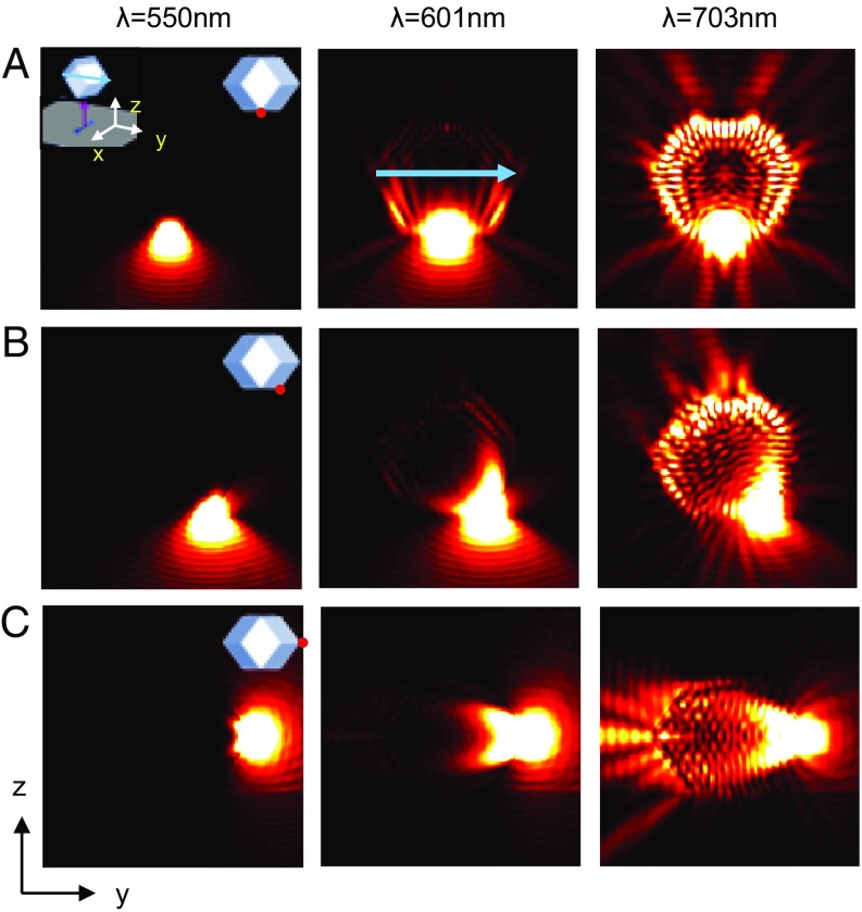
To understand this superlattice emission behavior (Fig. 2B), finite-difference time-domain (FDTD) (18) simulations and nanophotonic calculations (17, 19) were performed to explain the effects of RD microcavity scattering and nanoparticle surface plasmons, respectively (Theoretical Analysis of Superlattice Microcavity Emission Behavior and Fig. S3). The FDTD electrodynamics simulations were performed using dipole sources in an RD geometry to simulate emission from individual lattice sites (Fig. 3; Theoretical Analysis of Superlattice Microcavity Emission Behavior, Microcavity Scattering Profile []; Theoretical Analysis of Superlattice Microcavity Emission Behavior, Excitation Laser Intensity Profile in Microcavity []; and Theoretical Analysis of Superlattice Microcavity Emission Behavior, EMT Approximation). Because each lattice site is a gold nanoparticle surrounded by a dye layer, each site can be considered a plasmonically influenced dipole emitter (16, 17). Importantly, the superlattices were illuminated in transmission mode in the experiment (Fig. 2A). The laser can only excite a limited volume of the superlattice on the illuminated side (bottom of superlattice in Fig. 3 and Fig. S4; Theoretical Analysis of Superlattice Microcavity Emission Behavior, Excitation Laser Intensity Profile in Microcavity []; and Theoretical Analysis of Superlattice Microcavity Emission Behavior, EMT Approximation) because the laser light (λ ∼ 504 nm) strongly couples to surface plasmons of the nanoparticles and is absorbed. Therefore, the observed profiles (Fig. 2B) are constructed by emission from the excited volumes. Near-field profiles of single-dipole emission in the excited volume reveal strong spectral dependence of light transmission through the superlattice (Fig. 3 and Figs. S5 and S6). Near the LSPR frequency, emitted light is mostly directed away from the superlattice and only shallow penetration into the superlattice is observed due to strong plasmonic absorption (Fig. 3, Left). Far from the LSPR frequency (>600 nm, Fig. 3, Right), the light is transmitted through the superlattice and then emitted in various directions that are determined by the photonic properties of the RD, similar to what might be expected for a dielectric microcavity. Interestingly, depending on the position of the dipoles, high near-field intensity is observed just beneath the surface of the RD (Fig. 3A, Right and Fig. S6). This is due to internal reflection and indicates the existence of resonant modes similar to whispering-gallery modes (WGMs) found in spherical microcavities (2, 3). Such modes with the RD shape should not be surprising because WGMs exist in various 2D anisotropic microcavities (15, 20), and not just in circular ones. These observations suggest the possibility of using such architectural control to design 3D plasmonic microcavities with spatially and spectrally defined emission properties. Indeed, the RD shape can result in complex 3D WGMs at wavelengths longer than the LSPR frequency, and when such lattices are combined with a silver coating, moderate Q factors (>102) are possible (14). Importantly, the controllable exciton–plasmon interaction afforded by DNA-directed assembly makes it possible to exploit two intrinsically different cavity functions: the strong plasmonic near field around the LSPR wavelength (the dye–particle interaction), and the dielectric-cavity behavior at wavelengths longer than the LSPR frequency (the RD crystal habit).
Fig. S3.
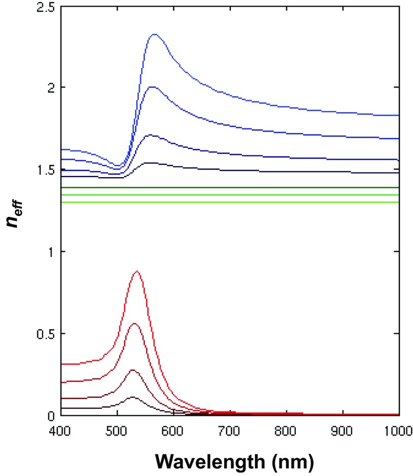
Real (blue) and imaginary (red) parts of the effective refractive index calculated by EMT. The gold FFs are 2%, 5%, 10%, and 15%. The bluer (redder) the lines are, the higher the FF is. The constant values (green) are the effective refractive indices after removing the gold nanoparticles from the lattices with FF = 10%, 20%, and 30%. The lighter the lines are, the higher the FF is.
Fig. 3.
Simulated microcavity near-field emission profiles. (A) FDTD-simulated near-field emission profile () of a dipole at the bottom of a superlattice microcavity. The microcavity center is (x,y,z) = (0,0,0), L is 5 µm, and the gold FF is 6%. (Left Inset) Microcavity orientation with respect to the coordinates as in Fig. 1. The incident direction of the excitation laser is indicated by a red arrow below the RD geometry. (Right Inset) Dipole (red dot) location, in the y–z plane, at the bottom of the RD geometry right beneath the facet. is indicated by a blue arrow. Three dipole orientations aligned with the x, y, and z axes were used and were averaged incoherently over these orientations. Three wavelengths are presented to show the behaviors close to and away from the LSPR frequency. Intensity around each dipole was purposely saturated based on the same scaling scheme to show light scattering throughout the RD shape. A substrate (n = 1.44) was added below the RD shape. (B and C) The same type of data as in A for two other dipole locations. All of the dipole sources were in the y–z plane beneath the surface of the RD shapes. Fig. S6 for emission profiles in the x–z plane.
Fig. S4.
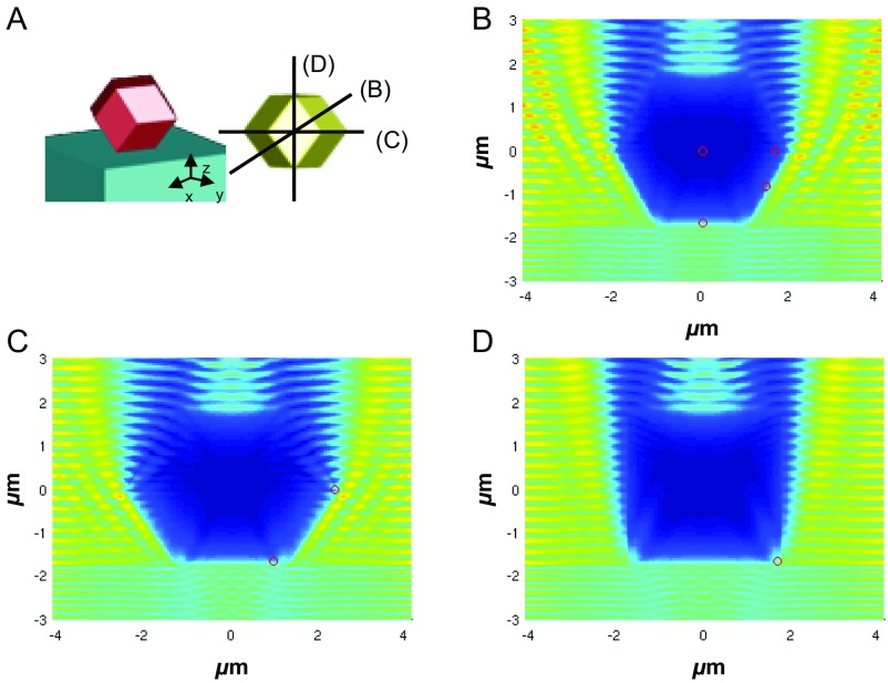
(A) Scheme showing a superlattice deposited on a substrate (Left) and a top view showing three cross-sections whose excitation light intensity is analyzed. (B–D) FDTD-calculated scattering profiles () of a microcavity with plane-wave injection. The cavity center is (x,y,z) = (0,0,0) and = 5 µm, and the gold FF is 6%. The wavelength is λ = 505 nm, and only several locations (red circles) of dipoles are chosen, not including other equivalent locations considering the symmetry. The contributions from those equivalent locations were added by reusing the calculated intensity from chosen locations (red circles).
Fig. S5.
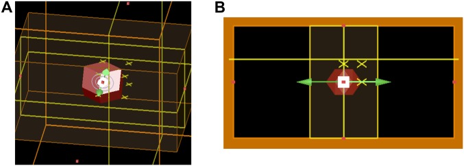
(A) Three-dimensional CAD image showing an FDTD setup with a dipole light source used to analyze dye emission scattering through the RD geometry. The arrow indicates the location and the orientation of a dipole source placed in the RD geometry. To calculate the near-field intensity, three 2D monitors (yellow) are placed parallel with and perpendicular to the optical axis in the experiment. A glass substrate is also inserted when necessary. (B) A 2D top view of the 3D image in A. The vertical direction corresponds to the optical axis of the microscope used in the experiment.
Fig. S6.
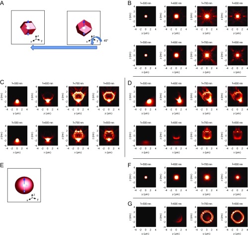
(A) Scheme showing the orientation of the RD considered in the main text (Left) and another with more symmetry (Right). The RD on the right and its orientation show the symmetry under 90° rotations with respect to x, y, and z axes as well as under reflection with respect to each plane (x–y, y–z, z–x). The orientation on the left can be achieved by rotating the RD on the right around the y axis by 45°. (B) FDTD-calculated emission profile () of a dipole at the center of the RD geometry in x–z (Top Row) and y–z (Bottom Row) planes. The microcavity center is (x,y,z) = (0,0,0) and = 5 µm, and the gold FF is 6%. The profiles are generated by incoherently averaging intensity over three dipole orientations aligned to the x, y, and z axes. (C and D) The same type of data as in B for the dipole locations presented in Fig. 3 A and B. (E–G) The same type of data for a spherical microcavity. F and G correspond to B and D, respectively.
Based on the predicted microcavity scattering behavior in the near field (Fig. 3), theoretical spatio-spectral profiles (Fig. 2B, Right) were constructed to explain the directional emission of the superlattice microcavities. In this process, the near-field scattering profiles of multiple dipoles at the bottom of the microcavity were projected into the far field (Theoretical Analysis of Superlattice Microcavity Emission Behavior, Microcavity Scattering Profile []; and Theoretical Analysis of Superlattice Microcavity Emission Behavior, Excitation Laser Intensity Profile in Microcavity []). The intrinsic dye emission spectrum (Alexa Fluor 532) and the nanoscale effect of coupling the dye to surface plasmons (leading to both enhancement and suppression of fluorescence) were incorporated into our theoretical models (Theoretical Analysis of Superlattice Microcavity Emission Behavior, Quantum Yield [q(λ)] and Enhanced Decay Rates of a Dye Around a Gold Nanoparticle; Fitting of the Theoretical Spatio-Spectral Emission Profile []) (17, 19). Significantly, at long wavelengths and with the superlattice out of focus, the superlattice profile (Fig. 2B, Bottom) shows high intensity at the center of the superlattice. Careful FDTD analysis at multiple focal plane positions (Fig. S7) reveals a clear light convergence in front of the microcavity. This is due to the directional scattering behavior of the microcavity which vertically projects and focuses emitted light from the excited volume (Fig. 3 A and B, Right and Fig. S6). On the other hand, emitted light from the side vertices (Fig. 3C, Right), which couples to the microcavity, is projected horizontally, and therefore, is not detected by the objective lens at long wavelengths. Close to the LSPR wavelength, emitted light from the side vertices is clearly visible (Fig. 2B, Bottom) due to strong plasmon-driven light emission in three dimensions (Fig. 3C, Left). On the other hand, the intensity at the center of the microlens close to the LSPR wavelength is very low for all focal planes (Fig. 2B and Fig. S7) due to light absorption by surface plasmons (Fig. 3, Left). These spectrally modulated directional scattering behaviors are the result of the combined effects of the RD microcavity shape and the plasmonic nature of the microcavity medium. These properties of the microcavities are important and may prove useful for constructing light-emitting devices with plasmon-driven spectral modulation and directional light emission. Indeed, the 3D geometry-driven lensing effect can focus light close to the superlattice without additional microoptical elements, thereby functioning as a local light source in larger devices. The spectral modulation provides tunability, allowing one to change the nature of light emission from scattered patterns (close to the LSPR frequency) to vertically/horizontally collimated ones (far from the LSPR frequency) by properly choosing the dye wavelength.
Fig. S7.
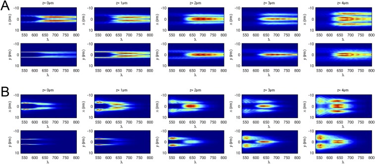
(A) Spatio-spectral emission profiles generated with far-field projections of the fields on the monitor perpendicular to the optical axis. The dye spectrum and near-field plasmonic influence on the dye spectrum are not included to solely show the microcavity scattering profile. The top (bottom) images are collected from 1D spatial domain perpendicular to (parallel with) of the microcavity (Fig. 1, Right). The microcavity center is (x,y,z) = (0,0,0) and = 5 µm, and the gold FF is 6%. The focal plane of far-field projection lens was varied (z = 0–4 µm). The profiles are generated by incoherently averaging intensity over multiple dipole locations in the excited volume (Theoretical Analysis of Superlattice Microcavity Emission Behavior, Excitation Laser Intensity Profile in Microcavity []) and three dipole orientations aligned to the x, y, and z axes. (B) The same type of data as in A after incorporating the dye emission spectrum influenced by surface plasmon (Theoretical Analysis of Superlattice Microcavity Emission Behavior, Quantum Yield [q(λ)] and Enhanced Decay Rates of a Dye Around a Gold Nanoparticle; Fitting of the Theoretical Spatio-Spectral Emission Profile []).
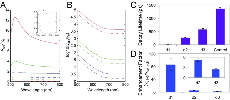
With these superlattice microcavities, one can systematically control the dye-to-gold nanoparticle distance by adjusting the point of covalent attachment of the dye to the DNA linker strands (Fig. 1, Left). Such control allows one to finely tune exciton–plasmon interactions (16, 17), which is important for emission engineering (7, 16) in regard to various parameters of interest such as decay rate and quantum efficiency. Microcavities with plasmonically active nanomaterials confined in 3D (nanoparticles) can exhibit orders-of-magnitude better light confinement (7) compared with 1D or 2D counterparts (e.g., nanosheets and nanorods). Therefore, nanophotonic calculations focused on exploring nanoparticle dye–exciton interactions (as described in Theoretical Analysis of Superlattice Microcavity Emission Behavior, Quantum Yield [q(λ)] and Enhanced Decay Rates of a Dye Around a Gold Nanoparticle; Fitting of the Theoretical Spatio-Spectral Emission Profile [], Fig. 4 A and B, and Figs. S8 and S9) show large decay enhancement factors at shorter wavelengths (<600 nm), with strong LSPR absorption (Fig. 4B). By carefully choosing the dye–gold surface distance via DNA design and the dye emission frequency, the quantum efficiency and the enhancement factor can both be optimized for desired applications.
Fig. 4.
Nanoparticle influenced dye temporal response. (A) Theoretically predicted (17) plasmon-enhanced radiative decay rates of dipoles normalized by their intrinsic radiative decay rate. Three different dye-to-nanoparticle surface distances are shown (1, 5, and 11 nm; d1, d2, and d3; red, green, and blue, and Theoretical Analysis of Superlattice Microcavity Emission Behavior, Quantum Yield [q(λ)] and Enhanced Decay Rates of a Dye Around a Gold Nanoparticle; Fitting of the Theoretical Spatio-Spectral Emission Profile []). Solid lines (dashed lines) indicate perpendicular (parallel) dipole orientations. (B) A similar data set for absorption (nonradiative) decay rates as in A. (C and D) Measured decay lifetimes and corresponding enhancement factors of d1–d3 superlattices with Alexa Fluor 700 dye. Photons were collected at 700 nm by a TCSPC system coupled to the microspectrophotometer (Optical Experiments, Single Superlattice Decay Lifetime Measurement and Fig. 2A). Rapid rate enhancement was observed as the dye–nanoparticle distance decreased. Decay lifetime of the Alexa Fluor 700 dye in silica was used to measure the intrinsic decay lifetime.
Fig. S8.
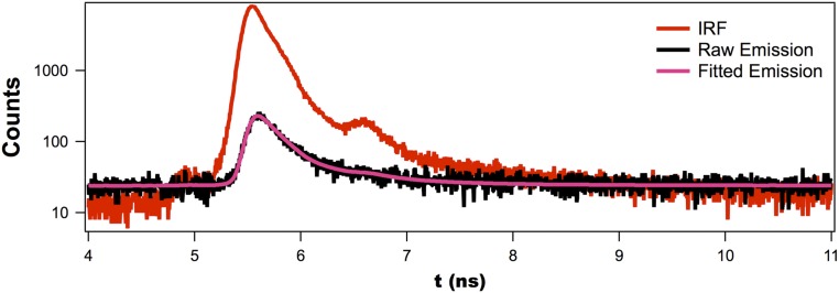
Example of decay pattern fitted with a biexponential decay model by deconvoluting the instrument response function (IRF). Here, an Alexa Fluor 700 coupled d3 superlattice.
Fig. S9.
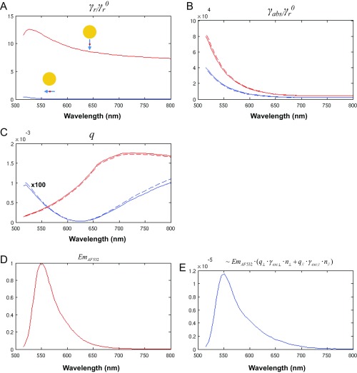
(A) Theoretically calculated γr with a 1-nm dye–gold surface distance (7). The diameter of the nanoparticle is 20 nm. Perpendicular (red) and parallel (blue) dipole orientations are presented. (B) γabs based on the same configuration in A. Calculation based on another paper (6) (dashed lines) is added to confirm the theory in ref. 7 (solid lines). (C) Quantum yields, , based on A and B. Due to its magnitude, the quantum yield for the parallel dye orientation is multiplied by 100. (D) Measured emission spectrum of Alexa Fluor 532 dye molecules. (E) The factor that modulates the spatio-spectral profile in the spectral domain: . The factor, , is normalized to be 1.
To demonstrate the tunability of exciton–plasmon interactions, superlattices were also synthesized with Alexa Fluor 700 dye. Alexa Fluor 700 was chosen to avoid extremely high enhancement factors associated with metal absorption around the LSPR frequency (Fig. 4B), which would cause the dye lifetime to fall below the instrumental detection limit and result in low quantum efficiencies. Measurement of time-resolved emission using a time-correlated single-photon counting (TCSPC) system (Optical Experiments, Single Superlattice Decay Lifetime Measurement and Fig. S8) shows a dramatic reduction in lifetime from the control sample (dyes coupled to DNA strands in silica), to the d3 superlattice, and further to the d1 superlattice (Fig. 4C). Here, the d1 superlattice lifetime is at or below the instrument detection limit (∼10 ps; Methods). The measured enhancement factors (Fig. 4D) were comparable to calculated values (Fig. 4 A and B) (17) and were also in range of observations made for similar nanostructures (16). Because the dye orientations with respect to gold surfaces are unknown, the observed lifetimes are likely values averaged over multiple dye orientations and perhaps influenced by dye–dye interactions (17). Although microcavity modes of the superlattices can contribute to the accelerated decay behavior (2), we ignore such effects in this work due to their low Q factor (5, 7). Further investigation is necessary to correlate the effect of microcavity modes on Purcell factors (∼Q/V) by increasing Q factors with higher gold volume fractions or silver surface-coated systems (14). Such superlattice microcavities can function as 3D hybrid plasmonic microcavities that exhibit both WGMs with high Q factors and strong mode confinement of nanoparticles (small V) with a wide spectral range (7), leading to high Purcell factors (∼Q/V) for applications such as plasmon lasing.
This work has laid the foundation for preparing dye-functionalized DNA plasmonic nanoparticle superlattices with unusual optical properties that derive from the microscale crystalline architectures and the placement of the molecular and nanoscale components within such architectures. These initial proof-of-concept structures unambiguously show that one can obtain plasmonically modulated directional light emission. Moreover, the exciton–plasmon coupling can be fine-tuned by using the DNA linkers as programmable scaffolds to strategically position both the particles and the dyes. The DNA-guided approach to superlattice microcavities described herein provides a versatile platform for building photonic architectures with exciton emission behavior that can be modulated in the spatial, spectral, and time domains for various nano-/microphotonic applications.
Methods
FDTD Calculation.
The FDTD simulations were performed with Lumerical FDTD solutions v.8.12.
Effective Medium Theory Approximation.
Effective medium theory (EMT) approximation is used to approximate the refractive indices of superlattices based on the Maxwell–Garnett equation, , where εeff, εinc, and εhost are dielectric constants of superlattices, gold, and silica host medium, and FF is the gold volume fraction.
Optical Experiments.
Microspectrophotometry was performed using a 504-nm pulsed laser (Picoquant). The measurements were made using a 50× objective (N.A. 0.8, Zeiss) and a CCD (Princeton Instruments) coupled to a spectrometer (Princeton Instruments). The signal was normalized by spectra of the CCD quantum efficiency and filter sets. Decay lifetime measurements were performed by coupling the microspectrophotometry system to a TCSPC system (Picoquant) via an optical fiber.
TCSPC Lifetime Detection Limit.
Through discussions with Picoquant, the limit was confirmed to be ∼10 ps based on the time scales of the detector, the pulse laser, and the TCSPC electronics.
See Supporting Information for details of experimental and theoretical methods used in this work.
Dye-Coupled Plasmonic Superlattice Microcavity Fabrication
Dye-Labeled DNA Synthesis.
DNA strands (Table S1) were synthesized on a MerMade 48 automated oligonucleotide synthesizer with reagents from Glen Research. Specifically, Amino Modifier C6 dT was incorporated into the DNA sequence at various points to label locations at which Alexa Fluor (Thermo Scientific) dye molecules would later be conjugated.
The synthesized DNA was then purified with reverse-phase high-performance liquid chromatography (HPLC) and characterized by matrix-assisted laser desorption ionization time-of-flight mass spectrometry (MALDI-TOF-MS). Purified DNA strands 3 to 8 were then labeled with Alexa Fluor 532 or Alexa Fluor 700 NHS Ester. The dye-labeled DNA was purified and characterized again with HPLC and MALDI-TOF-MS, respectively.
DNA Nanoparticle Conjugate Preparation.
Thiolated DNA strands 1 and 2 were treated with 100 mM DTT (Sigma-Aldrich) and subsequently desalted with size-exclusion chromatography (NAP-5, GE Healthcare). The DNA was then added to 20-nm citrate-capped Au nanoparticles (BBI) in a 4 nmol DNA to 1 mL nanoparticle ratio. The particles were allowed to incubate for 3 h, after which SDS and NaPO4 were added. NaCl was then added to the nanoparticle solution over the course of several hours until a final 0.5 M NaCl concentration was reached. Excess DNA was removed from the DNA nanoparticle solution with three rounds of centrifugation.
DNA strand 9 was added to strands 3 to 8 in equivalent amounts. The DNA was heated to 52 °C for 30 min and subsequently cooled to room temperature. This DNA was then added in a 175-linker per nanoparticle ratio to their respective strand 1 and 2 labeled Au nanoparticles. At this point, the system was heated at 45 °C for 30 min and cooled overnight. To quantify the number of bound dye strands per nanoparticle, the nanoparticle–dye solution was centrifuged and the fluorescence of the supernatant was quantified and compared with a standard curve with known dye concentrations to find on average 118 dye-labeled linker strands conjugated to each nanoparticle.
With the linker strands attached to the nanoparticles, nanoparticles with strand 1 were mixed with the equivalent nanoparticles labeled with strand 2 DNA. To allow the nanoparticle aggregates to reach their thermodynamically stable state, the aggregates were placed in a thermocycler (Applied Biosystems) and heated to 50 °C, after which the temperature was reduced by 0.1 °C every 10 min until the sample reached 25 °C. Control samples were also prepared with nanoparticle aggregates that did not undergo additional heat treatments and nanoparticle aggregates that were annealed below their annealing temperature as determined with temperature-dependent UV-vis spectroscopic experiments (Cary 5000, Agilent).
The samples above were then silica embedded where 2 μL of N-trimethoxysilylpropyl-N,N,N-trimethylammonium chloride (Gelest, 50% in methanol) was added to the nanoparticle aggregate solution. The sample was shaken (Eppendorf Thermomixer) for ∼20 min at room temperature to allow for association between the trimethylammonium cation and the negative phosphate backbone on the DNA. Next, 4 μL of triethyoxysilane (Sigma-Aldrich) was added and the sample was shaken at 700 rpm for at least 24 h. The samples were then rinsed in water and drop-cast on indium tin oxide-coated quartz substrates. Nanoparticle spacings of assembled structures were characterized with SAXS at Argonne National Laboratory’s APS.
Optical Experiments
Single Superlattice Emission Spatio-Spectral Analysis.
A microspectrophotometer was used for spatio-spectral analysis by detecting the emission signal from the individual superlattices (Fig. S1). Here, a Zeiss Axio Observer.Z1m microscope system was used. A picosecond pulsed laser (λ = 504 nm, minimum pulse width = 112 ps, Picoquant) was used to excite the dye molecules in the superlattices in transmission mode, and a Xenon lamp (XBO 75, λ = 300–1,100 nm) was used for imaging in reflection mode. The pulsed laser was coupled to the microscope system via a homemade optomechanical system with micrometer-scale xyz positioning and focusing (100× objective) capabilities. The pulsed laser was operated at a repetition rate of 40 MHz with a pulse energy of 3 nJ. The microscope image at the center of Fig. S1 shows a superlattice on a substrate and a defocused pulse laser spot generated by the 100× objective lens. The experiment was performed with a laser spot size similar to that of the superlattices (∼5–10 µm). The emission signal was collected by a 50× objective lens (N.A. = 0.8) and the pulse laser light was rejected by long-pass filters. A slit was used with a spectrometer (Princeton Instruments, Acton Series, 50 g/mm) to provide spectral resolution and to extract the emission signal from a thin area cutting through the center of superlattices. Typically, the long axis of the superlattice (Fig. 1, Right) is aligned to this area to study scattering properties. A CCD (Princeton Instruments, PyLoN) was used, and the collected spectra were normalized by the quantum efficiency of the CCD and the transmittance of long-pass filters to generate the data in Fig. 2 and Fig. S2. To confirm the experimental scattering behavior of the superlattices with that predicted by simulations, the focal plane of the 50× objective lens was moved with a step size of several micrometers. Fig. S2 shows spatio-spectral profiles of various control samples: d2 superlattice, d3 superlattice with an irregular orientation (vertex upward, Fig. 1), and annealed (polycrystalline) d1 and d3 superlattices (all with Alexa Fluor 532 dye). As predicted, the annealed superlattices (Fig. S2 C and D) do not show the typical triangular pattern (Fig. S2A and Fig. 2B) due to the lack of a well-defined shape. Lastly, the sample with an irregular orientation (vertex upward) does not show the triangular pattern due to a different angular scattering behavior.
Single Superlattice Decay Lifetime Measurement.
Decay lifetimes of the individual superlattices were measured by coupling a TCSPC (Picoquant FluoTime300) system to the microspectrophotometer via a fiber coupling system (Fig. S1). The emission signal from the superlattices was transported through an optical fiber to a monochromator which selects a particular wavelength for photon counting. To collect signals only from a single superlattice of interest, the laser pulse was focused onto a micrometer-scale spot to illuminate the superlattice.
To quantify decay lifetimes of the dyes distributed within the superlattices, reconvolution fitting was performed; this deconvolutes the time-domain profile of the pulsed laser from that of the dye. This was accomplished by measuring the lifetime of the laser without a sample present and using these data for subsequent lifetime fitting. Due to plasmon-induced fast decay of excitons in the superlattices (<100 ps), which is comparable to the laser pulse width, the accuracy of the quantified lifetime drops as the dye–Au distance becomes small. Fig. S8 shows a representative lifetime analysis data for a d3 superlattice with Alexa Fluor 700.
Theoretical Analysis of Superlattice Microcavity Emission Behavior
The superlattice emission behavior is a complicated problem to model involving multiple microoptical and plasmonic aspects such as microcavity light scattering and plasmonic effects on dye emission. We approximated this problem by separating the micrometer-scale phenomena (microcavity scattering) and the nanoscale phenomena (emission from each crystal site: nanoparticle–dye complex). To specifically address each component, we can model the spatio-spectral emission profile as , where is an RD microgeometry scattering profile for dipole emitters inside the superlattices, is the emission spectrum of the dye (Alexa Fluor 532), and are quantum yield and excitation rate of dyes around a gold nanoparticle, respectively, and is intensity of the excitation laser light within the RD microgeometry. FDTD simulations were performed to understand the RD microgeometry scattering and intensity distribution of the laser excitation in the RD [ and ], and analytical calculations were performed to predict the emission profiles of individual crystal sites, .
Microcavity Scattering Profile [].
FDTD simulations were performed with a commercial package (Lumerical FDTD Solutions v.8.12). To analyze the scattering behavior of dye emission through the RD microcavity geometry, an electric dipole source was placed in a micrometer-scale RD object (Fig. S5). Because all of the crystal sites can emit light, the simulation was performed with multiple dipole source positions in the microcavity volume where the excitation source intensity is high (see Theoretical Analysis of Superlattice Microcavity Emission Behavior, Excitation Laser Intensity Profile in Microcavity [] and the main text), and the individual dipole results were integrated over that volume to produce the total superlattice effect. At each dipole position, the calculation was performed with three (x, y, z) dipole orientations to simulate all of the orientations of the emitter. Due to the large spectral width of the dye emission and narrow width of the laser source, the emission signals from each dipole location and orientation were integrated incoherently [i.e., intensity summation rather than field summation for the RD microgeometry scattering, , with a weighting factor of the laser intensity distribution in the RD, ]. The perfectly matched layer boundary condition was used to absorb electromagnetic fields at the simulation boundary. Two monitors were added to capture the near-field intensity of two cross-sections that pass through the center of the RD geometry, and, in the experiment, these cross-sections are parallel to the optical axis of the microscope system (Fig. S1). One more monitor was added perpendicular to the above two monitors and its near-field information was postprocessed by a far-field projection with N.A. = 0.8 to simulate the effect of the 50× objective lens used in the experiment. Due to computational limitations, the optical medium of the bcc gold nanoparticle superlattices was approximated by EMT (see Theoretical Analysis of Superlattice Microcavity Emission Behavior, EMT Approximation below) with 6% gold volume fraction (FF) rather than including the nanoparticles explicitly. The effect of moving the objective lens along the optical axis was simulated by another postprocessing step using a chirped z transform. When necessary, a dielectric substrate (refractive index = 1.44) was added to include the effect of a glass slide.
Fig. S6 shows near-field intensity profiles of a microcavity (L = 5 µm). (Fig. 3 shows similar patterns with a substrate.) The profile with a dipole at the center of the RD (Fig. S6B) shows a purely radial profile of emission with several preferred emission angles. On the other hand, the profiles based on dipoles close to the surface of the RD (Fig. S6 C and D) show strong emission directionality and obvious interference patterns below the surface. A control simulation with a spherical shape (diameter = 5 µm) (Fig. S6 F and G) shows an isotropic pattern of emission for a dipole at the center and whispering-gallery–like resonant pattern for a dipole close to its surface, as often analyzed in the literature (3).
Fig. S7A shows far-field projected images (spatio-spectral profiles) at multiple objective lens focal plane locations. Because the result is based on the RD microgeometry scattering and laser intensity distribution in the RD [ and ] without dye information [e.g., and ], the intensity is distributed over the entire spectral range with a plasmonic signature at long wavelengths. Particularly, the profile based on the collection angle parallel with in the experiment (Fig. S7A, Bottom) exhibits a light focusing profile at z = 2–4 µm. This can be visualized with the wide–narrow–wide spatial distribution of light at long wavelengths, indicating a lens-like projection of emission from the excited volume. Based on these results, as the dye emission profile and plasmonic effect are incorporated (see Theoretical Analysis of Superlattice Microcavity Emission Behavior, Quantum Yield [q(λ)] and Enhanced Decay Rates of a Dye Around a Gold Nanoparticle; Fitting of the Theoretical Spatio-Spectral Emission Profile []), the experimentally observed spatio-spectral profile is approximated with reasonable consistency (Fig. S7B).
Excitation Laser Intensity Profile in Microcavity [].
In the experiment, the pulse laser light is injected and distributed in the microcavity. The laser light distribution determines the excited microcavity volume. Therefore, the intensity distribution profile functions as a weighting factor [] that is convoluted into the integration of each dipole emission profile to predict the experimental results. To calculate this, an FDTD simulation similar to Theoretical Analysis of Superlattice Microcavity Emission Behavior, Microcavity Scattering Profile [] was performed to approximate the intensity distribution of the excitation laser light in the RD geometry. For this purpose, a total-field scattered-field source (similar to a plane-wave source) was used. The intensity distributions in three different cross-sections along the optical axis (Fig. S4A) were recorded around the pulse laser wavelength. Those three cross-sections include all of the facet centers and most of the vertices. Therefore, by locating dipoles on those cross-sections, we can ensure an even distribution of dipoles.
Fig. S4 shows a representative intensity distribution () inside the microcavity with the excitation source injected from the substrate side (Fig. S4A). A drastic decrease in intensity toward the light propagation direction is observed due to strong plasmon-driven absorption. Due to such behavior, the excited volume becomes a shallow layer at the illuminated side. Therefore, vertices and facet centers were chosen as the locations of dipole sources (red circles, Fig. S4 B–D).
EMT Approximation.
In this work, we adopt EMT (21, 22) to approximate the refractive indices of superlattices to reduce calculations within the simulation volume. EMT can accurately describe the effective refractive indices of superlattices when the interparticle near-field coupling is negligible and the resonance of individual nanoparticles is mainly dominated by their dipolar resonance. These conditions are typically met when the volume fraction of the inclusion is less than 20% and the diameter of the inclusion is small (23). The superlattices in this work satisfy these criteria. EMT describes the dielectric constants of the superlattices with the Maxwell–Garnett equation, , where εeff, εinc, and εhost are dielectric constants of the effective superlattice medium, inclusion, and silica host medium, respectively. Here, , where r is the radius of gold nanoparticles and a is the bcc lattice constant. The dielectric function of gold was adopted from experimental data (24), and the refractive index of the silica host medium in the superlattices was assumed to be 1.43 in this work. Fig. S3 shows the real and imaginary parts of the effective refractive indices with several different gold volume fractions. The peak positions of the real parts are close to the surface plasmon resonance frequency, and they are red-shifted slightly at higher gold volume fractions. Overall, the real and imaginary parts increase at higher volume fractions due to the increase in polarizability of the effective medium. This sharp increase in the real and imaginary parts of the index is responsible for strong absorption and scattering around the surface plasmon resonance frequency.
Quantum Yield [] and Enhanced Decay Rates of a Dye Around a Gold Nanoparticle; Fitting of the Theoretical Spatio-Spectral Emission Profile [].
The quantum yield (q) and radiative and absorption rates of a single dye molecule around a metal nanoparticle have been theoretically formulated in other papers (17, 19). We adopt calculations from ref. 7 and apply them to our system taking into consideration the geometrical configuration. The quantum yield of a single dye molecule around a metal nanoparticle can be written as , where q0, γr0, γr, and γabs are intrinsic quantum yield, an intrinsic radiative decay rate, an induced radiative decay rate, and a rate of metal absorption, respectively. A decay channel, that of metal absorption, is introduced with the presence of a nanoparticle. γr and γabs need to be calculated to quantify quantum yield, and they are heavily dependent on geometric configurations such as nanoparticle size, metal surface–dye distance, and the dye orientation with respect to the metal surface. When the nanoparticle size and the metal surface–dye distances are determined, one can consider two primary dye orientations: perpendicular and parallel to the metal surface. For example, the radiative decay rate for the perpendicular dye–Au nanoparticle surface orientation can be written (17) as , where ε, a, and z are the dielectric constant of gold, the radius of the gold nanoparticle, and the distance between the gold surface and the dye, respectively. γr and γabs for our system are shown in Fig. 4 in the main text with two orientations. Fig. S9 shows q, γr, and γabs used for predicting the experimental result with a 1-nm dye–gold surface distance (Fig. 2 B and C and Fig. S7B). The intrinsic quantum yield (q0) was taken from the company database (Thermo Scientific, q0= 0.61) for Alexa Fluor 532.
The intrinsic dye molecule emission profile for Alexa Fluor 532 [] was obtained by measuring an emission profile of dye molecules in water. A Jobin Yvon Fluorolog FL3-22 fluorometer was used with a 500-nm excitation (Fig. S9D).
Based on the quantum yield and measured dye emission profile, we can complete the modeled spatio-spectral profile: . The contribution depends on the dye orientation (17), and the other contributions, , are consistently applied to all of the orientations. Therefore, we approximate: , where and are the populations of dye molecules that are perpendicular and parallel to the gold surface, respectively. Because and are not known, we consider the ratio between and as a fitting parameter to fit the theoretical spatio-spectral emission profile, , to those from the experiments. Note that these contributions ( and ) do not depend on wavelength (single-frequency information at λ = 504 nm).
Acknowledgments
Materials synthesis work was supported by Air Force Office of Scientific Research Award FA9550-12-1-0280 and Asian Office of Aerospace Research and Development Award FA2386-13-1-4124. It is also based upon work supported as part of the Non-equilibrium Energy Research Center and the Center for Bio-Inspired Energy Science, Energy Frontier Research Centers funded by the US Department of Energy (DOE), Office of Science, Office of Basic Energy Sciences under Awards DE-SC0000989 and DE-SC0000989-0002. The theory work was supported by National Science Foundation (NSF) Grant CHE-1465045. This work made use of the Electron Probe Instrumentation Center, Keck-II, and/or Scanned Probe Imaging and Development facility(ies) of Northwestern University’s NUANCE Center, which has received support from the Soft and Hybrid Nanotechnology Experimental (SHyNE) Resource (NSF NNCI-1542205); the Materials Research Science and Engineering Center program (NSF DMR-1121262) at the Materials Research Center; the International Institute for Nanotechnology (IIN); the Keck Foundation; and the State of Illinois, through the IIN. Small-angle X-ray scattering (SAXS) experiments were carried out at the Dupont–Northwestern–Dow Collaborative Access Team beam line at the Advanced Photon Source (APS), Argonne National Laboratory, and use of the APS was supported by the DOE (DE-AC02-06CH11357). J.C.K. acknowledges the Department of Defense for a National Defense Science and Engineering Graduate Fellowship. L.S. is grateful for a Ryan Fellowship from IIN. N.P.S. acknowledges support as an Alfred P. Sloan Research Fellow.
Footnotes
The authors declare no conflict of interest.
This article contains supporting information online at www.pnas.org/lookup/suppl/doi:10.1073/pnas.1619802114/-/DCSupplemental.
References
- 1.Yamamoto Y, Tassone F, Cao H. 2000. Semiconductor Cavity Quantum Electrodynamics (Springer, Berlin), p viii, 154 pp.
- 2.Vahala KJ. Optical microcavities. Nature. 2003;424(6950):839–846. doi: 10.1038/nature01939. [DOI] [PubMed] [Google Scholar]
- 3.Vollmer F, Arnold S. Whispering-gallery-mode biosensing: Label-free detection down to single molecules. Nat Methods. 2008;5(7):591–596. doi: 10.1038/nmeth.1221. [DOI] [PubMed] [Google Scholar]
- 4.Sandoghdar V, et al. Very low threshold whispering-gallery-mode microsphere laser. Phys Rev A. 1996;54(3):R1777–R1780. doi: 10.1103/physreva.54.r1777. [DOI] [PubMed] [Google Scholar]
- 5.Tame MS, et al. Quantum plasmonics. Nat Phys. 2013;9(6):329–340. [Google Scholar]
- 6.Oulton RF, et al. Plasmon lasers at deep subwavelength scale. Nature. 2009;461(7264):629–632. doi: 10.1038/nature08364. [DOI] [PubMed] [Google Scholar]
- 7.Genov DA, Oulton RF, Bartal G, Zhang X. Anomalous spectral scaling of light emission rates in low-dimensional metallic nanostructures. Phys Rev B. 2011;83(24):245312. [Google Scholar]
- 8.de Leon NP, et al. Tailoring light-matter interaction with a nanoscale plasmon resonator. Phys Rev Lett. 2012;108(22):226803. doi: 10.1103/PhysRevLett.108.226803. [DOI] [PubMed] [Google Scholar]
- 9.Macfarlane RJ, et al. Nanoparticle superlattice engineering with DNA. Science. 2011;334(6053):204–208. doi: 10.1126/science.1210493. [DOI] [PubMed] [Google Scholar]
- 10.Auyeung E, et al. DNA-mediated nanoparticle crystallization into Wulff polyhedra. Nature. 2014;505(7481):73–77. doi: 10.1038/nature12739. [DOI] [PubMed] [Google Scholar]
- 11.Jones MR, et al. DNA-nanoparticle superlattices formed from anisotropic building blocks. Nat Mater. 2010;9(11):913–917. doi: 10.1038/nmat2870. [DOI] [PubMed] [Google Scholar]
- 12.Zhang C, et al. A general approach to DNA-programmable atom equivalents. Nat Mater. 2013;12(8):741–746. doi: 10.1038/nmat3647. [DOI] [PubMed] [Google Scholar]
- 13.Auyeung E, Macfarlane RJ, Choi CH, Cutler JI, Mirkin CA. Transitioning DNA-engineered nanoparticle superlattices from solution to the solid state. Adv Mater. 2012;24(38):5181–5186. doi: 10.1002/adma.201202069. [DOI] [PubMed] [Google Scholar]
- 14.Park DJ, et al. Plasmonic photonic crystals realized through DNA-programmable assembly. Proc Natl Acad Sci USA. 2015;112(4):977–981. doi: 10.1073/pnas.1422649112. [DOI] [PMC free article] [PubMed] [Google Scholar]
- 15.Wiersig J. Hexagonal dielectric resonators and microcrystal lasers. Phys Rev A. 2003;67(2):023807. [Google Scholar]
- 16.Reineck P, et al. Distance and wavelength dependent quenching of molecular fluorescence by Au@SiO2 core-shell nanoparticles. ACS Nano. 2013;7(8):6636–6648. doi: 10.1021/nn401775e. [DOI] [PubMed] [Google Scholar]
- 17.Bharadwaj P, Novotny L. Spectral dependence of single molecule fluorescence enhancement. Opt Express. 2007;15(21):14266–14274. doi: 10.1364/oe.15.014266. [DOI] [PubMed] [Google Scholar]
- 18.Taflove A, Hagness SC. 2005. Computational Electrodynamics: The Finite-Difference Time-Domain Method (Artech House, Boston), 3rd Ed, p xxii, 1006 pp.
- 19.Gersten J, Nitzan A. Spectroscopic properties of molecules interacting with small dielectric particles. J Chem Phys. 1981;75(3):1139–1152. [Google Scholar]
- 20.Chang ASP, et al. Visible three-dimensional metallic photonic crystal with non-localized propagating modes beyond waveguide cutoff. Opt Express. 2007;15(13):8428–8437. doi: 10.1364/oe.15.008428. [DOI] [PubMed] [Google Scholar]
- 21.Bergman DJ. Dielectric-constant of a composite-material - problem in classical physics. Phys Rep. 1978;43(9):378–407. [Google Scholar]
- 22.Ruppin R. Evaluation of extended Maxwell-Garnett theories. Opt Commun. 2000;182(4-6):273–279. [Google Scholar]
- 23.Ross MB, Blaber MG, Schatz GC. Using nanoscale and mesoscale anisotropy to engineer the optical response of three-dimensional plasmonic metamaterials. Nat Commun. 2014;5:4090. doi: 10.1038/ncomms5090. [DOI] [PubMed] [Google Scholar]
- 24.Johnson PB, Christy RW. Optical constants of noble metals. Phys Rev B. 1972;6(12):4370–4379. [Google Scholar]


