

Abstract
The mechanism by which Cu catalyst pretreatments control graphene nucleation density in scalable chemical vapor deposition (CVD) is systematically explored. The intrinsic and extrinsic carbon contamination in the Cu foil is identified by time-of-flight secondary ion mass spectrometry as a major factor influencing graphene nucleation and growth. By selectively oxidizing the backside of the Cu foil prior to graphene growth, a drastic reduction of the graphene nucleation density by 6 orders of magnitude can be obtained. This approach decouples surface roughness effects and at the same time allows us to trace the scavenging effect of oxygen on deleterious carbon impurities as it permeates through the Cu bulk. Parallels to well-known processes in Cu metallurgy are discussed. We also put into context the relative effectiveness and underlying mechanisms of the most widely used Cu pretreatments, including wet etching and electropolishing, allowing a rationalization of current literature and determination of the relevant parameter space for graphene growth. Taking into account the wider CVD growth parameter space, guidelines are discussed for high-throughput manufacturing of “electronic-quality” monolayer graphene films with domain size exceeding 1 mm, suitable for emerging industrial applications, such as electronics and photonics.
Introduction
Scalable, controlled crystal growth of graphene and related 2D materials is the foremost challenge and enabling factor for any technology exploiting their unique properties. Chemical vapor deposition (CVD) can uniquely address the demand for integrated manufacturing and is emerging as the industrially dominant growth technique for “electronic-grade” mono- or few-layer large-area films of 2D materials.1,2 For graphene, the CVD process is typically catalytic; i.e., it is based on an elevated temperature gas exposure of a planar catalytic surface, which aids the dissociation of the gaseous precursor and the formation of a graphitic lattice.3 Cu is one of the most widely used catalyst materials for graphene CVD growth, providing a rather error-tolerant window for monolayer graphene formation at high gas exposures (>1 mbar) and at temperatures typically close to the melting point of Cu.4−6 Under these conditions, the Cu surface is extremely dynamic, and while the understanding of the growth mechanisms remains incomplete, what is known is that graphene domains nucleate isothermally on the Cu surface.7,8 Moreover, the microstructure of the resulting monolayer graphene film directly links to the nucleation density and how the graphene domains evolve and merge.3,9 The macroscopic graphene film properties depend to varying degrees on the graphene domain size, connectivity, and the domain-boundary structure including related defects.10−12 Therefore, a key aspect of CVD process development is to control graphene nucleation effectively.10−15 In the emerging industry, the use of polycrystalline Cu foils is cost-efficient and widely adopted.16,17 For graphene growth on such polycrystalline Cu foils, it has been established that under most CVD conditions graphene does not preferentially nucleate at the Cu grain boundaries, neither do the lateral grain dimensions of the Cu surface limit the size of graphene domains.18−20 The ever increasing body of literature on graphene nucleation control on polycrystalline Cu foils indicates that foil pretreatment is of paramount importance, whereby two main lines of treatment have emerged: surface etching/electropolishing21−23 and the addition of oxygen.14,19,24−26 It is widely demonstrated that graphene typically nucleates heterogeneously at defects, surface steps, and impurities on the Cu surface,21,23,27 while the rationale for both treatment methods is eliminating or passivating these nucleation sites. However, given the complexity of polycrystalline Cu surfaces combined with the highly dynamic nature of the Cu surface at elevated temperatures during CVD and the limited understanding of the graphene growth process, the causality and detailed effects of the various pretreatments remain largely unclear. While rolling striations in commercial Cu foils are well documented to cause an increased and preferential graphene nucleation, the general statement that reducing Cu surface roughness reduces the graphene nucleation density is less straightforward. This is because the state of the Cu surface during CVD is typically unknown and low graphene nucleation densities can be found on Cu surfaces that are relatively rough (compared to the atomic thinness of the graphene) before and after CVD. Numerous reports highlight the effects of oxygen in Cu-catalyzed graphene CVD, and the causality arguments range from cleaning the Cu surface25,26,28−30 to passivating Cu active sites and changing the catalytic dehydrogenation properties of the Cu surface.14,19 Moreover, the oxygen pretreatment protocols vary from preoxidizing the Cu foil and heating in an inert atmosphere14,24,25,29 to dosing oxygen directly before graphene growth.19,26
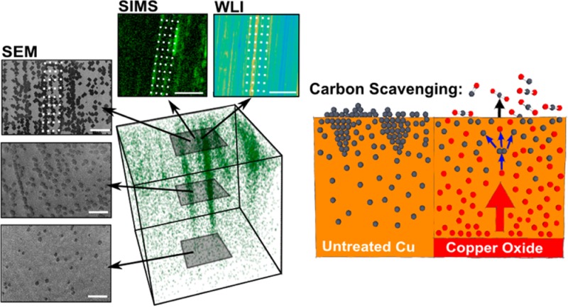
Here, we systematically investigate and compare the most widely used polycrystalline Cu catalyst pretreatments in order to elucidate their role in the catalytic graphene CVD process, in particular regarding the control over the monolayer graphene nucleation density. We therefore focus on widely used commercial cold-rolled Cu foils. Unlike thin Cu films (physical vapor deposited, e.g., on an insulating substrate), Cu foils do not show any significant additional surface roughening during the CVD process due to Cu grain growth.31 We devise a new simple method to study the effects of oxygen in this context by selectively oxidizing the “backside” of the Cu foil, i.e., the side of the Cu foil that is not used for graphene growth. This allows us to clearly decouple Cu surface roughness effects from chemical effects, triggered by oxygen permeation through the Cu bulk. Time-of-flight secondary ion mass spectrometry (ToF-SIMS) is used to depth-profile and surface-map the Cu foils after the various CVD process stages. This technique is able to provide high mass resolving power (>5000) at ppm detection levels in order to trace not only the oxygen and carbon contamination levels but also possible chemical contaminants in the Cu before and after the various etching and electropolishing procedures. Our data shows that as oxygen permeates through the bulk of the Cu foil it acts as a scavenger for carbon trapped in the Cu bulk and (sub-) surface regions. Therefore, oxygen scavenging not only deactivates nucleation sites ingrained into the Cu foil but also removes atmospheric adsorbents that, as we show here, also increase nucleation density. Parallels to well-known processes in metallurgy such as smelting in Cu refining are also considered. Through these ToF-SIMS investigations and surface roughness measurements, it was found that the redistribution as well as the removal25,26 of deleterious carbon, not a reduction in the surface roughness, was the critical factor to reducing the graphene nucleation density to below 1 mm–2. Our study is undertaken with a commercial CVD reactor, widely used within the nascent graphene industry, with 50 cm2 sized Cu foils over which graphene is grown homogeneously. The implications of these findings are discussed regarding high-throughput monolayer graphene CVD with domain sizes >1 mm. This understanding allows us to rationalize the many seemingly contradictory reports in the literature on this topic and devise generalized guidelines for the most efficient pretreatment methods for Cu-catalyzed graphene CVD.
Results
Motivated by its common use across the literature,14,19,24,25 we focus on 25 μm thick, polycrystalline Cu foil that is uncoated and preannealed as a model Cu catalyst (see Methods). A range of different pretreatments are employed to the Cu foil, and their effect on the foil roughness and graphene nucleation is studied, with the results summarized in Figure 1. The CVD exposure conditions for all pretreatment experiments are kept constant [growth temperature 1065 °C, with a gas mixture of CH4 (9 sccm, 0.1% diluted in Ar), H2, and Ar; see Supporting Information Figure S1]. The dependency on CVD conditions is discussed later. The pretreatments can be classified in three different approaches: (I) surface-etching of the catalyst to remove obvious contaminants, (II) (electro-)polishing to reduce the surface roughness, and (III) chemical surface/bulk Cu modification with oxygen. We here characterize the surface roughness by white light interferometry (WLI) (see Methods and Figure S2) and use the arithmetic mean Ra as quantitative measure for surface roughness.
Figure 1.

Overview of Cu pretreatments and the effect on graphene nucleation density (GND) and Cu surface roughness (Ra). Pretreatments are classified into categories I–III. (I) Pretreatments that remove/cover the contamination layer on the surface of the catalyst, i.e., surface etching, performed by floating the Cu foil on FeCl3 solution for different etching times (green triangles) and sputtering 250 nm Cu on top of the Cu foil (“PVD”, green star). (II) Pretreatments that reduce the Cu surface roughness, i.e., electropolishing, indicated by blue squares with increasing polishing times. The chemical mechanically polished (CMP) sample is shown as a blue pentagon. (III) Pretreatments utilizing oxygen, i.e., backside oxidization samples (BO), annealed in Ar are shown as red circles for various backside oxidation times. (b) Schematic indicating the cause of the reduction in nucleation density for surface pretreatments I–III.
As a representative technique for (I) we focused on wet-etching by floating the Cu foil on a 0.5 M FeCl3 solution for times tI between 15 and 75 s, where the etched depth is proportional to tI (see Figure S3). As shown in Figure 1, when the Cu surface is etched with FeCl3, Ra increases up to 550 nm for tI = 30 s, which corresponds to approximately 150 nm of Cu removal. No further increase in Ra is observed for longer etching times. Note that Ra is defined here as the macroscopic surface roughness, and the Ra value measured before CVD is also a good indicator of the macroscopic surface roughness at high temperatures. This can be shown by comparing Ra values before and after high-temperature annealing (see Figure S4), and we find that both values are in close correlation. Figure 2a shows scanning electron microscopy (SEM) images of the Cu surface after the graphene CVD process for increasing tI. For the untreated Cu foil, graphene domains preferentially nucleate along the Cu rolling striations (Figure 2a(i)), which is well-documented in the literature.26,29,32 The graphene nucleation density (GND) of the untreated sample, as characterized by SEM, is 1.4 × 104 mm–2. The GND significantly decreases with increasing time tI (Figure 2a(ii)–(iii)), and a roughly 2 orders of magnitude reduction in GND with respect to untreated Cu foils is found for tI = 45 s. Furthermore, the 2D and 3D ToF-SIMS carbon maps of the untreated Cu foil in Figure 2 show a clear carbon enrichment at the Cu surface along the rolling striations. The average carbon content decreases with increasing depth and saturates to a base value for the intrinsic carbon at about 150–200 nm in the Cu foil. As Figure 1 highlights, the increase in Ra from 310 to 560 nm with increased Cu surface etching (I) actually leads to a decrease in the GND. This implies that GND is predominantly dependent on the residual carbon concentration at the surface rather than just the catalyst surface roughness. With surface etching method (I), the GND can be decreased to a value of 5.5 × 102 mm–2 but not significantly further, as highlighted in Figure 1.
Figure 2.
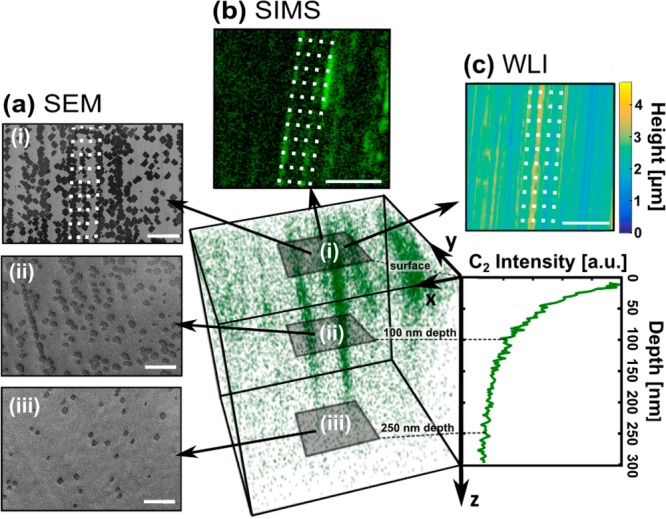
ToF-SIMS measured carbon impurities in the Cu foil before graphene growth and its correlation to graphene nucleation density (GND) after graphene growth. (a) Scanning electron microscopy (SEM) images (i)–(iii) correspond to graphene growth on the Cu surface that is (i) untreated, (ii) 100 nm FeCl3 etched, and (iii) 250 nm FeCl3 etched in the z-direction. The 3D C2– map and corresponding carbon depth profile illustrate the carbon distribution within the untreated Cu foil. (b) Surface ToF-SIMS map of C2– (green) from the first ∼5 nm of the Cu foil surface. (c) Topography of the untreated Cu foil measured by white light interferometry (WLI). The white dotted line represents a visual aid to show how graphene nucleates along a preferential direction, corresponding to areas of high carbon concentration and located along the rolling striations of the Cu foil, as shown in the SEM of graphene nuclei in (i), the ToF-SIMS C2– map of the Cu foil surface (b), and the Cu topography profile as measured by WLI (c). All scale bars are 50 μm; the 3D ToF-SIMS map is not to scale and corresponds to a volume of 150 × 150 × 0.3 μm3.
Another method to lower the average carbon content of the Cu surface while keeping Ra roughly constant is to deposit a Cu film via physical vapor deposition (PVD) on top of the Cu foil. Figure 1 shows that a reduction in GND to 2.6 × 103 mm–2 can be obtained by sputtering a 250 nm thick Cu film (see Methods) onto the untreated Cu foil. This is further evidence that the residual carbon concentration at the Cu surface plays a key role in regulating the GND. The reduction in GND is only modest since both the impurity diffusion and Cu interdiffusion are fast, at the growth temperatures used, such that impurities may segregate to the surface.
As a representative technique for (II), electropolishing of the Cu surface was performed. This not only removes the impurity layer as described in (I) but also reduces the Cu surface roughness. Electropolishing of the Cu foil was performed in a solution of phosphoric acid in DI water (10.3 M; see Methods). A voltage of 2.7 V was applied for times tp and varied between 0 and 450 s. It is observed that Ra remains constant for tp < 70 s, whereas longer tp leads to an increasingly smooth Cu surface (see also Figure S5). This change from predominately etching to surface smoothing at roughly tp = 70 s can be explained by the buildup of an “anodic film”.33−36 During electropolishing, cations (positive Cu ions) leave the Cu surface and become soluble in the electrolyte. This continues until the saturation limit is approached as metal ions only slowly diffuse to the cathode, thereby establishing a viscous layer at the anode. These heavy metal ions form the anodic film, therefore reducing the copper removal (etching) rate as the anodic film is already saturated with ions. Thus, as soon as the anodic film is established, the current density as well as the etch rate reduces and polishing of the Cu foil commences.33−36 This transition from etching to polishing is highly dependent on the polishing solution, temperature, and geometry of the electropolishing setup. Most reports on electropolished Cu foils for graphene growth use a phosphoric acid-based solution, albeit at widely different dilutions and working voltages.21−23,37,38Figure 1 shows that electropolishing (method II) led to a reduction in GND to 2.5 × 102 mm–2 for tp < 70 s even though Ra remained approximately constant. The reduction in GND was similar in magnitude to method I, which indicates that the reason for this GND reduction is the removal of surface contamination. For extended electropolishing times such as tp = 450 s, Ra was reduced to 180 nm, causing a decrease in GND to 57 mm–2. Figure 1 highlights a clear trend in this range that samples with smaller Ra exhibit a lower GND. In order to show how far the GND can be reduced by method II, a chemical mechanical polished (CMP) Cu substrate was used with surface roughness of Ra = 3 nm. Graphene growth on the CMP sample resulted in a GND of 8.3 mm–2 (Figure 1); i.e., method II allows a GND reduction of roughly 3 orders of magnitude compared to the untreated case. This indicates that after removing the surface contamination there is indeed a region (highlighted in blue in Figure 1a,b) where the GND can be reduced by only reducing Ra.
Cu oxidation is another method to chemically modify not only the Cu surface but also the bulk of the foil. Most of the literature that highlights the effects of oxygen in Cu-catalyzed graphene CVD uses an oxidizing gas atmosphere. However, by oxidizing the growth surface, both Ra and the concentration of other chemical surface species are changed.29,39 In order to decouple these effects and to clearly highlight the role of oxygen, the selective wet-chemical oxidation of the backside of the Cu foil is used as method III. To oxidize only the backside, the Cu foil was floated on the surface of a 30% H2O2 solution heated at 100 °C for times, tO, between 0 and 300 s (see Methods). For tO = 300 s, a Cu oxide thickness of roughly 70 nm is measured on the backside of the foil by ToF-SIMS (see Figure S8), which is roughly 1 order of magnitude thicker than the native oxide layer after air exposure for several weeks, which was found to be 3–5 nm by both XPS and ToF-SIMS. A range of more complex methods of applying an oxide on the backside (and/or front side), including air oxidation, cuprous-, cupric-, and copper hydroxide powders and sputtered copper oxides, were used, and all of these methods resulted in similar results. Furthermore, it should be noted that what we refer to as the backside of the Cu foil is the side of the foil that when loaded into the CVD reactor faced downward, i.e., toward the heater, whereas the graphene growth results reported here refer exclusively to the front side of the Cu foil that faced the CVD gas atmosphere. Some literature sometimes confusingly reports graphene growth on (what we refer to) the backside of the Cu foil or inside Cu foil pockets.39−42 In terms of future integrated graphene manufacturing, growth on the front side of the foil is most easily controlled and hence is in the focus of our discussion here. When these backside oxidized (BO) samples were heated in Ar (BO + Ar) (see Methods), a significant decrease in GND was observed for increased tO (Figure 1). For tO = 300 s, the GND was reduced by 6 orders of magnitude relative to the untreated Cu foil to a value of 2.7 × 10⁻² mm–2. Hence, Figure 1 highlights that the oxidation method (BO + Ar) clearly dominates all other pretreatment methods in terms of reduction in GND. It is noteworthy that this 6 orders of magnitude change in GND occurs for constant Ra, clearly highlighting that surface roughness is not the dominating effect for graphene nucleation.
When attempting to understand why this significant reduction in GND occurs for these BO samples and how this process affects other important parameters of the graphene CVD process, it should be noted that for the experimental conditions used here no increase in graphene growth rate was observed comparing samples with and without backside oxidation (see Figure S6). Previous literature speculated on the role of oxygen in the kinetics of catalytic hydrocarbon dissociation on Cu surfaces and reported increased graphene growth rates for oxygen-rich Cu.19 We do not observe a measurable increase in graphene growth rate with our oxidation methods under our conditions.43 Either way, the following question arises: what causes this significant change in GND for method III?
In order to identify potential mechanisms and to compare the chemical composition of the pretreated samples, ToF-SIMS measurements were performed on the samples after annealing. Each ToF-SIMS measurement was acquired by cyclically analyzing a 150 × 150 μm2 area from the center of a 400 × 400 μm2 sputtered region during the course of depth profiling to mitigate crater edge effects. Profiles were acquired up to a depth of approximately 250 nm (for more information, see Methods). Figure 3 shows three-dimensional ToF-SIMS maps, which give insight into the carbon distribution in the respective Cu foils after annealing. A clear difference in carbon distribution can be observed between the samples. The Ar:H2 and Ar annealed samples show areas of high local carbon density, in particular along the rolling striations. In contrast to this, for the BO + Ar sample the carbon distribution is homogeneous across the surface region and no such areas of high carbon localization are found.
Figure 3.
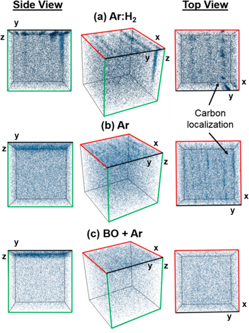
Three-dimensional ToF-SIMS maps of C2– in the Cu foil after (a) Ar:H2 annealing, (b) Ar annealing, and (c) Ar annealing of a backside oxidized sample (BO + Ar). The z-axis sputter depth is 185 nm, the xy-plane is 150 × 150 μm2, and the C2– signal is plotted in blue. All samples are annealed at 1065 °C for 30 min and subsequently cooled to room temperature in Ar (see Supporting Information Section 1). For the Ar:H2 and Ar annealed samples, localization of carbon along rolling striations is found in the surface region, whereas for the BO + Ar case a homogeneous carbon distribution is found. A reduced bulk C2– intensity is also observed for the BO + Ar sample (see Figure S9b).
From the C2– ion signal, we extract the local surface carbon density frequency distribution in order to quantify variations across the different samples, i.e., we define a control volume of 3 × 3 × 3 pixels (which equates to 2.56 μm × 2.56 μm × 10.8 nm) and compute the carbon density per control volume for the first ∼20 nm of the Cu surface. In line with Figure 3, the carbon density frequency distribution (Figure 4) shows that in the BO + Ar samples there are significantly less areas of high local carbon density.
Figure 4.
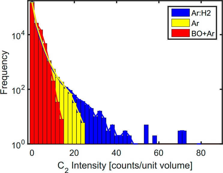
Frequency distribution of the carbon density for Ar:H2, Ar, and backside oxidized + Ar (BO + Ar) annealed samples. The values are determined using the 3D ToF-SIMS data for C2– and a control volume of 3 × 3 × 3 pixels for the first ∼20 nm of the surface. The BO + Ar sample shows significantly less regions of high carbon density compared to Ar:H2 and Ar samples. The areas of high carbon density in the Ar:H2 and Ar samples correspond to the carbon localizations shown in Figure 3.
The BO + Ar treatment leads to a reduction in the oxide at the backside of the Cu foil;44,45 thus, if the BO + Ar sample is removed from the CVD reactor, only a native oxide is found. However, if the BO + Ar sample (now without oxide on the backside) is placed back (after a period tair where the sample was stored in air) into the reactor and CVD graphene growth is performed, we still find that the GND is several orders of magnitude lower than the untreated (UT) Cu foil (see Figure 5). Moreover, we find that the GND is dependent on tair. The GND of the BO + Ar sample is 2.7 × 10⁻² mm–2, exposing the BO + Ar annealed sample to air for only tair = 5 min increases the GND in the subsequent growth experiment by approximately 1 order of magnitude to 3.7 × 10⁻¹ mm–2. After 10 days of air storage (tair = 10 days) the GND is 14 mm–2, which is a similar order of magnitude to the electropolished sample with tp = 450 s, where GND = 57 mm–2 (see also Figure 1).
Figure 5.
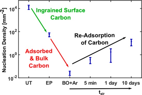
Graphene nucleation density (GND) as a function of Cu pretreatment. The untreated Cu foil (UT) shows the highest GND, followed by an electropolished (tp = 450 s) Cu foil (EP). The backside oxidation (BO + Ar) treatment without cooling and removing the sample from the reactor results in the lowest GND. However, if after BO + Ar annealing the reactor is cooled to room temperature and the sample is removed from the reactor for a time tair of 5 min to 10 days, the GND increases with increasing tair.
This systematic exploration of the effects of three different but relevant approaches to Cu pretreatment (methods I–III) under fixed CVD growth conditions provides a detailed understanding of how and why the Cu foil should be prepared to endeavor to reduce the GND. However, one of the challenges for CVD growth optimization is that the parameter space is multidimensional, including aspects of reactor design and flow regime. In addition, it is well documented in the literature that temperature, carbon precursor partial pressure, and its ratio to hydrogen can have a significant influence on the GND.4,14,29,46−48 Our results of different pretreatment approaches summarized in Figure 1 are based on a growth temperature of 1065 °C and a growth atmosphere of 250 sccm Ar, 26 sccm H2, and 9 sccm CH4 (0.1% diluted in Ar). Industrial high-throughput CVD not only requires a low GND but also reasonably high growth rates to grow continuous films. Figure 6 highlights that this requires a compromise. In line with other reports, we use a growth temperature close to the Cu melting point, which is known to lower the GND as well as result in a higher growth rate.5,49−52 However, regarding the carbon precursor concentration the compromise becomes obvious: a low GND requires low precursor concentration, whereas a high growth rate requires a high precursor concentration. It is beyond the scope of this article to explore all detailed dependencies on CVD growth parameters. However, to make this important point regarding GND versus growth rate, we simplistically look at the variation of CH4 flow rate while other conditions are kept constant. The BO + Ar pretreatment case is considered here, which, as established above, dominates all other pretreatment methods in terms of reducing the GND. For the other pretreatment cases, similar dependencies will apply.
Figure 6.

(a) Correlation between graphene domain size and required growth time for neighboring domains to begin to merge on Cu foil after backside oxidation (BO + Ar) pretreatment, as indicated by the blue dashed line. Different CH4 flow rates (VCH4) are shown as solid lines for the use of 0.1% diluted CH4 in Ar. Literature (Wu16,54 Wu15,18 Eres,29 Wang14,55 Chen13,37 Chen15,43 Lin,56 Miseikis,42 Zhou,14 and Yan1257) values are included for graphene growth on polycrystalline foil and homogeneous precursor exposure, with the exception of Wu15,18 where local precursor feeding was used. (b) A Cu foil after graphene growth performed with 20 sccm CH4 (0.1% diluted in Ar) and a growth time of 8 h with BO + Ar treatment (to visualize graphene grains directly on the Cu foil, it was placed on a hot plate at 250 °C for 1 min58).
Increasing the CH4 flow rate from 7 to 75 sccm for the BO + Ar case results in a significant increase in GND from 1.6 × 10⁻² to 7.7 mm–2, reflecting a roughly exponential behavior (see Figure S11). It is well-known that the graphene growth rate is not constant throughout the growth process, in particular across different catalyst surfaces, and that extrapolating a growth rate from postgrowth graphene coverage can be misleading, based on, for instance, different nucleation times across polycrystalline catalyst foils.29,32,48,53 Nonetheless, we introduce the average graphene growth rate (AGR) defined by an average postgrowth graphene domain diameter divided by the time of hydrocarbon exposure as the simplest possible parameter. Figure S11 shows that such AGRs increase linearly with CH4 flow from 0.3 to 2.8 mm/h in the same 7–75 sccm interval.
This AGR can then be used to provide the simplest
of estimates
for the average diameter at which neighboring graphene domains will
start to merge, Dmerge =  , and the required growth time until the
point of domain merging, tmerge = Dmerge/AGR. The blue dotted line in Figure 6a illustrates this
dependency between tmerge and Dmerge for different CH4 flow rates
(VCH4). This blue dotted line
corresponds to the point where on average the first neighboring graphene
domains will start to merge, but in order to obtain a continuous graphene
film, longer growth times are required to ensure complete coverage
at all locations. Despite the crude nature of our estimates, the blue
dotted line offers a useful guide to the eye to highlight the aforementioned
required compromise in CVD conditions across the state-of-the-art
literature. In addition, Figure 6b shows that millimeter-sized graphene grains can be
obtained homogeneously on wafer-sized Cu foils in a commercial CVD
reactor using the BO + Ar pretreatment and carefully chosen process
parameters.
, and the required growth time until the
point of domain merging, tmerge = Dmerge/AGR. The blue dotted line in Figure 6a illustrates this
dependency between tmerge and Dmerge for different CH4 flow rates
(VCH4). This blue dotted line
corresponds to the point where on average the first neighboring graphene
domains will start to merge, but in order to obtain a continuous graphene
film, longer growth times are required to ensure complete coverage
at all locations. Despite the crude nature of our estimates, the blue
dotted line offers a useful guide to the eye to highlight the aforementioned
required compromise in CVD conditions across the state-of-the-art
literature. In addition, Figure 6b shows that millimeter-sized graphene grains can be
obtained homogeneously on wafer-sized Cu foils in a commercial CVD
reactor using the BO + Ar pretreatment and carefully chosen process
parameters.
Discussion
The catalytic dissociation of hydrocarbon in CVD graphene synthesis results in a carbon filling of the Cu surface and in the Cu bulk. This process is mediated by carbon diffusion into and out from the catalyst bulk.7,59,60 On reaching the carbon solubility limit, a further supply of carbon causes a supersaturation to occur, which leads to the nucleation and subsequent growth of graphene at the catalyst surface.7,32 If carbon is already present as contamination in the Cu catalyst before the precursor exposure, then surface supersaturation is achieved more readily. Such inhomogeneous enrichment of deleterious carbon, for instance, along Cu rolling striations, leads to a locally higher GND (see Figure 2). As all of our data clearly shows, the success of a pretreatment method largely depends on how well the carbon content of the Cu (in the bulk and surface region) can be reduced and controlled. We note that this discussion is specific to low-carbon solubility catalyst materials like Cu, which at the same time is not a highly active catalyst for amorphous/graphitic carbon dissociation and hydrocarbon dehydrogenation.61−64 Ni, Co, and Fe, for instance, which have a comparatively high carbon solubility, are much more highly active catalysts in these cases;65−68 the situation is distinctly different as deleterious surface carbon could readily dissociate and dissolve into the bulk.
Our ToF-SIMS depth profiles and surface maps of widely used 25 μm thick, polycrystalline Cu foils show that contamination is present up to a depth of 150–200 nm from the surface of the untreated catalyst. The removal of such a carbon-rich region by surface etching (method I) allows the GND to be lowered by roughly 2 orders of magnitude to a value of 5.5 × 102 mm–2 but not significantly further, as highlighted in Figure 1. It is worth emphasizing that removing more than 150–200 nm of the Cu surface does not further reduce GND. A similar level of GND reduction can be achieved by depositing a cleaner film of Cu (e.g., by PVD) on top of the Cu foil, which buries/dilutes the initially present carbon impurities. Equally, the high-temperature preannealing of Cu in, e.g., a hydrogen atmosphere has also been shown to reduce the GND to similar levels,57,69 which might be linked to the removal or in-diffusion of initially present surface carbon and residual trace carbon in the copper bulk.
Using method II, (electro)polishing of the catalyst surface, not only the top contaminated layer is removed but also the Cu surface roughness is reduced. The data clearly show that GND reduction by electropolishing is due to both the removal of surface carbon and the reduction in surface roughness, not just the latter, as is sometimes argued.21,22 Furthermore, Figure 1 shows that after the reduction of surface carbon contamination to bulk levels the GND can be reduced by another 1–2 orders of magnitude by reducing the surface roughness. Considering that CVD temperatures close to the Cu melting point are used, at which the metal surface diffusivity is extremely high and the catalyst surface is extremely dynamic, such dependency on surface roughness is not self-evident. Moreover, the macroscopic roughness, in contrast to microscopic roughness,7 does not readily or significantly alter during the CVD process (Figure S4). However, reducing macroscopic roughness of polycrystalline Cu foils will allow a reduction in GND to a certain level, as shown in Figure 1 for a Cu surface with a very low macroscopic roughness, i.e., the CMP Cu sample. This sample revealed a GND of 8.3 mm–2 for the CVD conditions described above. Macroscopic surface roughness values significantly lower than CMP samples are difficult to obtain practically and will allow little further reduction in GND. Nevertheless, a clear trend of lower GND with lower surface roughness was found in this region of the parameter space. On the one hand, the sole focus on surface roughness21−23,37,70 can be misleading and it is not the most important parameter for a pretreatment with a focus on reducing GND as shown in Figure 1. On the other hand, GND is not the only “quality” parameter and the macroscopic catalyst roughness can be deleterious as it translates into increased surface area for as-grown graphene films, which, after transfer, translates into increased wrinkles and tears in the graphene films.71Figure S7 shows a transferred PMMA/graphene stack on Si/SiO2 support before the PMMA is removed in acetone. The topography of the transferred PMMA/graphene stack reassembles the macroscopic Cu surface topography, shown in Figure 2c, although at a lower Ra value of 67 nm. This surplus surface area of graphene will lead to wrinkles after the PMMA is dissolved, causing the graphene layer to collapse onto the Si/SiO2 substrate. Such wrinkling can negatively impact many graphene properties;72,73 hence, there is a clear incentive to minimize the macroscopic roughness of the catalyst surface.
While pretreatment methods I and II investigate widely used approaches, method III introduces the selective wet-chemical oxidation of the backside of the Cu foil as a new simple method. Our systematic ToF-SIMS measurements show that method III leads to a redistribution of the carbon impurity present in the Cu foil. In particular, local areas of very high carbon concentration are removed and a homogeneous carbon profile is found after this pretreatment. Method III on its own allows a GND reduction of 6 orders of magnitude down to 2.7 × 10⁻² mm–2 and thus clearly dominates all other pretreatment methods in terms of reduction in GND. Since method III does not alter the roughness of the Cu (front) surface, it was clearly shown that this drastic effect relates to the permeation of oxygen species through the catalyst bulk. Given the high diffusivity of atomic carbon in Cu,40,74,75 it is surprising that the carbon profile of the Cu foils annealed at 1065 °C (in Ar:H2 and Ar) for 30 min still shows a carbon distribution with localizations in particular along the roiling striations (Figure 3). In contrast to atomic carbon, graphitic/amorphous or otherwise structured carbon does not as readily diffuse in the Cu bulk. Thus, it is likely that the areas of high carbon concentration correspond to graphitic or amorphous carbon species that were ingrained during the cold rolling process. Unlike transition metals like Ni, Co, and Fe, Cu is known to be a very poor catalyst not only for the dehydrogenation of hydrocarbon precursors but also for dissociating graphitic/amorphous carbon.61−64 Hence, deleterious solid surface carbon can remain on a Cu surface even at high temperatures. These amorphous/graphitic carbon impurities then result in a locally higher GND.
We propose that the mechanism by which oxygen redistributes carbon in the Cu foil links to Cu smelting, a process commonly used in large-scale extraction metallurgy. In the smelting process, Cu ores (usually sulfide minerals, e.g., chalcopyrite) are oxidized with oxygen enriched air at high temperature in order to drive oxygen into the Cu matte, which then leads to an oxidation of the unwanted impurities. These impurities segregate to the surface, forming the “slag”, or become volatile as SO2 and CO2.76 After smelting, the Cu matte contains 0.2–0.4% oxygen. This residual oxygen is subsequently removed by hydrocarbon reduction removal in a fire refining step.76−78 Thus, by first oxidizing the matte followed by a hydrocarbon injection, a relatively pure Cu metal is obtained.76
Figure 7 schematically outlines how the oxygen acts as a scavenging agent in method III in analogy to smelting, deactivating impurities in the Cu foil that lead to a local carbon supersaturation and thus act as graphene nucleation site. Heating in an Ar atmosphere leads to oxygen diffusion into the Cu bulk from the initially oxidized backside. In contrast to that, annealing in an H2 containing atmosphere can lead to a direct Cu reduction at the backside via the gas phase; hence, it does not lead to the same drastic effect since less oxygen diffuses into the Cu bulk. Previous studies have shown that Cu oxide (mainly cupric oxide CuO to begin with) initially decomposes to cuprous oxide (Cu2O) upon heating.7,25,28,44,79,80 At even higher temperatures, the oxide dissociates at the metal oxide interface (Cu2O(s)→ 2Cu(s) + O) and the oxygen dissolves into the bulk Cu.44,45,81 The oxygen then diffuses in the Cu bulk and can desorb from the surface (O(in Cu)→ 1/2O2(g)).45 Dissolved atomic oxygen is highly reactive and has been shown to promote hydrocarbon dissociation on Cu.67,78 This dissolved oxygen thereby scavenges carbon impurities by promoting the dissociation of solid carbon impurities in the Cu foil. This creates more mobile carbon species, leading to a homogeneous carbon profile across the Cu catalyst (see Figure 3). Oxygen desorbing from the surface may also oxidize adsorbed or surface bound carbon impurities, which then become volatile (in the form of CO and CO225). In fact, our SIMS data shows evidence of increased levels of oxidized carbon species such as C2O and isocyanate (cyano groups have been shown to react in the presence of oxygen at elevated temperatures to isocyanate (NCO)82−84) (see Figure S10). This represents a very effective way of removing deleterious carbon and to significantly reduce the GND. We have shown that this effect is independent of the specific backside oxidation method; rather, a sufficiently thick oxide film is required to provide enough oxygen. The diffusion process through the solid Cu bulk is fast enough given the 25 μm foil thickness used;85 however, when using much thicker Cu substrates, scaling of the process has to be considered.26
Figure 7.
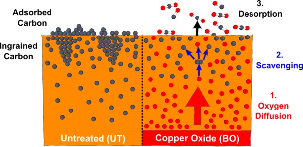
Illustration of the oxygen scavenging in Cu foils. An untreated Cu foil exhibits carbon impurities in the surface region as well in the bulk. An oxide layer can be grown on the backside of the Cu foil by floating the Cu foil on H2O2. Upon heating, the copper oxide reduces and oxygen can diffuse into the Cu foil. The dissolved oxygen scavenges the carbon impurities, resulting in a relatively carbon-free Cu foil without areas of high local carbon concentration.
Furthermore, we have observed that after the BO + Ar treatment the GND increases again as a function of air exposure time between the annealing step and the growth step, approaching a similar level as the electropolished Cu foil after several days (Figure 5). This indicates that not only the ingrained surface carbon impurities act as nucleation sites but also adsorbed (hydro-)carbon species drastically increase the GND on Cu. This also partially explains why electropolished foils show a higher GND compared to the BO + Ar treatment, as electropolishing removes only ingrained surface carbon impurities but carbon adsorption in the time period between electropolishing and graphene CVD will introduce additional nucleation sites. Note also that the BO + Ar treatment leads to a relatively lower C2– concentration in the bulk of the Cu foil (Figure S9b).
The role of other contamination species on the graphene growth should also be considered. However, our SIMS investigation did not show a correlation of other impurity species (i.e., Cl, S, and F) and GND for the above-described pretreatments.
Focusing on industrially relevant processing conditions, Figure 1 can serve as a clear guide to what order of GND reduction can be achieved with a given pretreatment approach. Nevertheless, to achieve the maximum domain size in a continuous graphene film, it is also important to consider the required growth time. In this context, Figure 6 illustrates the compromise between large average domain size and fast growth time for CVD graphene. State-of-the-art for standard CVD is that centimeter-sized graphene domains can be achieved but typically for growth times exceeding 1 day. Furthermore, for graphene electronic devices, at a given graphene channel size the likelihood of a grain boundary intersecting with the device area scales with the inverse of the graphene domain diameter and thus there are diminishing returns for increasing the domain size from, e.g., 5 mm to 1 cm (see Figure S12). Regarding the growth of a single graphene domain, this bottleneck can be overcome, for instance, by local gas exposure, as recently highlighted by Wu et al.18 We further emphasize that we consider here nonaligned graphene domain nucleation, which is commonly found for polycrystalline foil catalysts. For well-prepared catalyst surfaces, in particular single-crystal catalysts, collective graphene domain alignment can be achieved, and if all domains seamlessly merge, then a high GND can be afforded and monocrystalline graphene areas can be grown in short time.86,87 In this case, the aforementioned compromise lies more in the choice of (crystalline) catalyst, which can be more expensive and unsuitable for, e.g., industrial roll-to-roll manufacturing.
Conclusions
We systematically studied the most widely used pretreatment approaches for polycrystalline Cu catalyst foil and established what level of control they each allow over the monolayer graphene nucleation density as part of a scalable CVD process for large-area “electronic-grade” graphene films. By oxidizing the backside of the Cu foil, we have introduced a new simple pretreatment method, which allowed us to unambiguously show that the major effect of oxygen is to act as scavenging agent for deleterious carbon. The mechanisms of such carbon deactivation/removal have parallels to well-known processes in metallurgy such as smelting. We show that it is not the presence of oxygen but the redistribution and removal of initially present deleterious carbon that is key to a low graphene nucleation density, not just for a specific method but for all methods.
We have clearly mapped out the parameter space relevant to control the GND to a certain order of magnitude. Method I, the surface-etching of the catalyst to remove obvious contaminants, allows the GND to be lowered by roughly 2 orders of magnitude for our given conditions to a value of 5.5 × 102 mm–2 but not significantly further. A similar level of GND reduction can be achieved by depositing a cleaner film of Cu (e.g., by PVD) on top of the Cu foil, which buries/dilutes the initially present carbon impurities. For method II, including methods such as electropolishing, we showed that the GND reduction is due to both the removal of surface carbon and the reduction in surface roughness. Furthermore, our data indicates that reducing macroscopic roughness allows an additional 1–2 orders of magnitude reduction in GND, which here is down to 8.3 mm–2 for CMP Cu. Macroscopic surface roughness values significantly lower than for such CMP samples are difficult to obtain practically for metal foils and will allow little further reduction in GND. However, GND is not the only “quality” parameter, and macroscopic catalyst roughness can be deleterious as it translates into increased surface area for as-grown graphene films. This can translate into increased wrinkling and tears in the graphene film after transfer. General method III, based on chemical surface/bulk Cu modification with oxygen, was implemented via the backside oxidation process to decouple the chemical effects from, e.g., the effects of surface roughness. This pretreatment clearly dominated all other pretreatment methods in terms of reduction in GND. We could demonstrate that the simple backside oxidation triggered a 6 orders of magnitude reduction in GND down to 4.5 × 10⁻² mm–2 while the polycrystalline Cu surfaces maintained a macroscopic roughness of a few hundred nanometers. This highlights how robust and error-tolerant the catalytic CVD process can be, enabling atomically thin graphene single-crystal domains of macroscopic (>millimeter) dimensions being grown on a rough, polycrystalline metal support. We note that our measurements here refer to macroscopic and not microscopic roughness. The latter is often discussed in the framework of atomistic nucleation models, whereby it should be noted that the metal surface diffusivity is extremely high and the catalyst surface is extremely dynamic under the growth conditions.
Furthermore, the parameter space to control the GND in terms of catalyst pretreatment was mapped. Control of GND is in turn essential to grow large single crystalline graphene domains and to engineer the polycrystallinity and hence properties of continuous large-area graphene films. Our data establishes a clear framework of what level of graphene film control can be achieved for a given pretreatment. While each application might have its specific requirements on graphene “quality”, our data can be seen as guideline of minimum process requirements for cost-effective industrial graphene manufacture. For the simple nonepitaxial, single nucleation approach, there is a compromise between maximum domain size and growth time. While centimeter graphene domain dimensions are possible, the growth times required (>24 h) may be unfeasible in industrial graphene manufacturing. This is not a fundamental limit of CVD and can be overcome, for instance, by adopting local gas feeding or tailoring the catalyst surface to trigger collective graphene domain alignment, as already demonstrated in the literature.18,86,87
The understanding of the underlying mechanism and influence of Cu pretreatment on nucleation density can enable the establishment of alternative and generic routes for Cu pretreatment. For instance, electropolishing the front surface in combination with backside oxidation successfully removes impurities from the Cu foil while maintaining a low surface roughness. This approach circumvents the roughening of the carefully electropolished front side of the Cu foil (as can be the case in air oxidizing or in situ oxygen dosing as used previously14,19,24−26,29) while at the same time utilizing the oxide on the backside to scavenge carbon impurities.
Methods
As a growth catalyst, Alfa Aesar (46365) Cu foil with a thickness of 25 μm was used. The Cu purity specified by the manufacturer is 99.8% (metal basis); note that this purity value does not include elements such as carbon and oxygen. Surface roughness was measured with a Wyko NT1100 white light optical profiling system using 20× magnification in VSI mode. Scanning electron microscopy (SEM) pictures were taken with a Carl Zeiss SIGMA VP at an acceleration voltage of 2 kV. All CVD graphene growth experiments were performed in a commercial Aixtron Black Magic Pro 4 in. cold wall PECVD system with a base pressure of 0.05 mbar (more details on the CVD process are provided in the Supporting Information Section 1). Before the Cu catalyst is loaded into the CVD reactor, it was pretreated by several methods as discussed in the main text (see also Figure S1). Method I: Wet-etching of the Cu foil was performed by floating the Cu foil on a 0.5 M FeCl3 solution for times tI between 15 and 75 s. The Cu foil was hereby gently placed on top of the acid such that the topside was not exposed to the acid. Subsequently, the Cu foil was rinsed in DI water for 5 min and dried after IPA dipping with a N2 gun. Sputtering 250 nm Cu onto the Cu foil (PVD) was performed in a home-built sputter coater with a 99.999% purity target and a sputter rate of 0.5 nms–1. Method II: The CMP sample is a Cu polycrystalline substrate of 99.99% purity and 1 mm thickness. The roughness of the CMP sample is Ra = 3 nm, as specified by the manufacturer (MTI item number Cu101010S1-P). The electropolishing solution was prepared by mixing H3PO4 (85 wt % in H2O, Sigma-Aldrich) in a 7:3 ratio with DI water. The distance between cathode and anode is 4 cm. Electropolishing was performed for polishing times tp between 0 and 450 s. After electropolishing, the Cu foil was rinsed in a water jet for 5 min and then dried with N2 after IPA dipping. Method III: Wet oxidation of the Cu foil was performed on a 30% H2O2 solution (Fisher Scientific) heated at 100 °C for times tO between 0 and 300 s. The Cu foil was gently placed on the hydrogen peroxide such that the Cu foil floats and the top side is not exposed to hydrogen peroxide. Subsequently, the Cu foil was rinsed in DI water and IPA and dried with a N2 gun. If not otherwise stated, BO treatment refers to tO = 300 s and electropolishing refers to tp = 450 s. Between pretreatment and CVD growth, all samples were stored in a class 10000 cleanroom atmosphere for 2–4 weeks. In order to calculate the GND, the graphene growth was stopped at a growth time well before the graphene domains start to merge. Microscope or SEM pictures were then used to calculate the number of graphene nuclei per unit area (i.e., microscope-/SEM-picture magnification was chosen large enough to contain at least 10 graphene nuclei) on four different locations of the Cu foil.
Ex situ ToF-SIMS measurements were performed using a TOF SIMS IV instrument (ION-TOF Gmbh, Germany), at a vacuum pressure of <5 × 10⁻⁹ mbar. Each SIMS measurement was acquired by cyclically analyzing a 150 × 150 μm2 area (with 128 × 128 pixel density) from the center of a 400 × 400 μm2 sputtered region during the course of depth profiling to mitigate crater edge effects on the generated spectra. For sputtering cycles, 10 keV Cs+ ions with an ion current of 30 nA was used, with interleaved image spectra acquired using a 25 keV Bi3+ ions from a liquid metal ion gun, orientated at 45° to the sample surface, after each sputter cycle. This was operated at an ion current of 0.1 pA, in an interlaced mode with a cycle time of 100 μs. The depth of the profile was determined by acquiring reference profiles from a copper layer of known thickness, under the same profiling conditions. While surface roughness does have some impact on the lateral resolution of the SIMS images with increasing depth generated over the course of the measurements, due mainly to the orientation of the ion guns at 45° with respect to the samples. The sputter rate is essentially homogeneous across the surface, and the surface roughness was observed to propagate throughout the sputter process. This is an important consideration for understanding the distribution of material in the samples to rule out sputter induced modifications to the samples. Data processing was carried out by selecting relevant peaks in the ToF-SIMS spectra and monitoring their change in intensity over the course of the sputter profiling. Background subtraction was applied by subtracting a region of the spectra in close proximity to the peaks, with the same width as the peak. For comparison of the carbon content in the samples, in order to mitigate the contribution of adventitious carbon due to ambient exposure prior to measurement, the ions from the first ∼1.2 nm of the samples were excluded. This was determined by monitoring the H- and CH- ion signals during depth profiling and observing where they reached a local minimum at the surface of the samples. All spectra were normalized to the total ion intensity, using a spectrum-to-spectrum normalization, which allowed for the most consistent comparison between the samples. This is particularly necessary in these annealed samples as subtle variations in Cu crystal orientation across different Cu grains can lead to differences in the ion yield of different species, from sample to sample and even from location to location on the same sample. Normalizing to the total ion yield was shown to produce very similar profiles, with four measurements typically taken from each sample.
Acknowledgments
This research was supported by the ERC under grant InsituNANO (279342), the EPSRC under grant GRAPHTED (EP/K016636/1), and the Innovation R&D programme of the National Measurement System of the U.K. Department of Business, Innovation and Skills (project number 118616). We thank P. Kidambi, A. A. Sagade, R. Blume, R. Havelund, I. S. Gilmore, M. P. Seah, R. Langford, and J. J. Rickard for helpful discussions.
Supporting Information Available
The Supporting Information is available free of charge on the ACS Publications website at DOI: 10.1021/acs.chemmater.6b03241.
Experimental details (CVD process), additional characterizing data (foil roughness measurements, foil pretreatment etch and polishing details, SIMS data), extrapolated nucleation density and growth rate data, estimate of grain boundary intersection probability, CVD data for foils with different purity, and TEM diffraction data of graphene islands (PDF)
The authors declare no competing financial interest.
Supplementary Material
References
- Zurutuza A.; Marinelli C. Challenges and Opportunities in Graphene Commercialization. Nat. Nanotechnol. 2014, 9, 730–734. 10.1038/nnano.2014.225. [DOI] [PubMed] [Google Scholar]
- Vogel E. M.; Robinson J. A. Two-Dimensional Layered Transition-Metal Dichalcogenides for Versatile Properties and Applications. MRS Bull. 2015, 40, 558–563. 10.1557/mrs.2015.120. [DOI] [Google Scholar]
- Hofmann S.; Braeuninger-Weimer P.; Weatherup R. S. CVD-Enabled Graphene Manufacture and Technology. J. Phys. Chem. Lett. 2015, 6, 2714–2721. 10.1021/acs.jpclett.5b01052. [DOI] [PMC free article] [PubMed] [Google Scholar]
- Vlassiouk I.; Regmi M.; Fulvio P.; Dai S.; Datskos P.; Eres G.; Smirnov S. Role of Hydrogen in Chemical Vapor Deposition Growth of Large Single Crystal Graphene. ACS Nano 2011, 5, 6069–6076. 10.1021/nn201978y. [DOI] [PubMed] [Google Scholar]
- Li X.; Magnuson C. W.; Venugopal A.; An J.; Suk J. W.; Han B.; Borysiak M.; Cai W.; Velamakanni A.; Zhu Y.; et al. Graphene Films with Large Domain Size by a Two-Step Chemical Vapor Deposition Process. Nano Lett. 2010, 10, 4328–4334. 10.1021/nl101629g. [DOI] [PubMed] [Google Scholar]
- Li X.; Cai W.; An J.; Kim S.; Nah J.; Yang D.; Piner R.; Velamakanni A.; Jung I.; Tutuc E.; et al. Large-Area Synthesis of High-Quality and Uniform Graphene Films on Copper Foils. Science 2009, 324, 1312–1314. 10.1126/science.1171245. [DOI] [PubMed] [Google Scholar]
- Kidambi P. R.; Bayer B. C.; Blume R.; Wang Z.-J.; Baehtz C.; Weatherup R. S.; Willinger M.-G.; Schloegl R.; Hofmann S. Observing Graphene Grow: Catalyst-Graphene Interactions during Scalable Graphene Growth on Polycrystalline Copper. Nano Lett. 2013, 13, 4769–4778. 10.1021/nl4023572. [DOI] [PMC free article] [PubMed] [Google Scholar]
- Li X.; Cai W.; Colombo L.; Ruoff R. S. Evolution of Graphene Growth on Ni and Cu by Carbon Isotope Labeling. Nano Lett. 2009, 9, 4268–4272. 10.1021/nl902515k. [DOI] [PubMed] [Google Scholar]
- Seah C.-M.; Chai S.-P.; Mohamed A. R. Mechanisms of Graphene Growth by Chemical Vapour Deposition on Transition Metals. Carbon 2014, 70, 1–21. 10.1016/j.carbon.2013.12.073. [DOI] [Google Scholar]
- Tsen A. W.; Brown L.; Levendorf M. P.; Ghahari F.; Huang P. Y.; Havener R. W.; Ruiz-Vargas C. S.; Muller D. a; Kim P.; Park J. Tailoring Electrical Transport across Grain Boundaries in Polycrystalline Graphene. Science 2012, 336, 1143–1146. 10.1126/science.1218948. [DOI] [PubMed] [Google Scholar]
- Yazyev O. V.; Louie S. G. Electronic Transport in Polycrystalline Graphene. Nat. Mater. 2010, 9, 806–809. 10.1038/nmat2830. [DOI] [PubMed] [Google Scholar]
- Yu Q.; Jauregui L. a; Wu W.; Colby R.; Tian J.; Su Z.; Cao H.; Liu Z.; Pandey D.; Wei D.; et al. Control and Characterization of Individual Grains and Grain Boundaries in Graphene Grown by Chemical Vapour Deposition. Nat. Mater. 2011, 10, 443–449. 10.1038/nmat3010. [DOI] [PubMed] [Google Scholar]
- Song H. S.; Li S. L.; Miyazaki H.; Sato S.; Hayashi K.; Yamada A.; Yokoyama N.; Tsukagoshi K. Origin of the Relatively Low Transport Mobility of Graphene Grown through Chemical Vapor Deposition. Sci. Rep. 2012, 2, 337. 10.1038/srep00337. [DOI] [PMC free article] [PubMed] [Google Scholar]
- Zhou H.; Yu W. J.; Liu L.; Cheng R.; Chen Y.; Huang X.; Liu Y.; Wang Y.; Huang Y.; Duan X. Chemical Vapour Deposition Growth of Large Single Crystals of Monolayer and Bilayer Graphene. Nat. Commun. 2013, 4, 2096. 10.1038/ncomms3096. [DOI] [PubMed] [Google Scholar]
- Grosse K. L.; Dorgan V. E.; Estrada D.; Wood J. D.; Vlassiouk I.; Eres G.; Lyding J. W.; King W. P.; Pop E. Direct Observation of Resistive Heating at Graphene Wrinkles and Grain Boundaries. Appl. Phys. Lett. 2014, 105, 143109. 10.1063/1.4896676. [DOI] [Google Scholar]
- Kobayashi T.; Bando M.; Kimura N.; Shimizu K.; Kadono K.; Umezu N.; Miyahara K.; Hayazaki S.; Nagai S.; Mizuguchi Y.; et al. Production of a 100-M-Long High-Quality Graphene Transparent Conductive Film by Roll-to-Roll Chemical Vapor Deposition and Transfer Process. Appl. Phys. Lett. 2013, 102, 023112. 10.1063/1.4776707. [DOI] [Google Scholar]
- Bae S.; Kim H.; Lee Y.; Xu X.; Park J.-S.; Zheng Y.; Balakrishnan J.; Lei T.; Kim H. R.; Song Y. Il; et al. Roll-to-Roll Production of 30-Inch Graphene Films for Transparent Electrodes. Nat. Nanotechnol. 2010, 5, 574–578. 10.1038/nnano.2010.132. [DOI] [PubMed] [Google Scholar]
- Wu T.; Zhang X.; Yuan Q.; Xue J.; Lu G.; Liu Z.; Wang H.; Wang H.; Ding F.; Yu Q.; et al. Fast Growth of Inch-Sized Single Crystalline Graphene from a Controlled Single Nucleus on Cu-Ni Alloy. Nat. Mater. 2015, 15, 43–47. 10.1038/nmat4477. [DOI] [PubMed] [Google Scholar]
- Hao Y.; Bharathi M. S.; Wang L.; Liu Y.; Chen H.; Nie S.; Wang X.; Chou H.; Tan C.; Fallahazad B.; et al. The Role of Surface Oxygen in the Growth of Large Single-Crystal Graphene on Copper. Science 2013, 342, 720–723. 10.1126/science.1243879. [DOI] [PubMed] [Google Scholar]
- Nguyen V. L.; Lee Y. H. Towards Wafer-Scale Monocrystalline Graphene Growth and Characterization. Small 2015, 11, 3512–3528. 10.1002/smll.201500147. [DOI] [PubMed] [Google Scholar]
- Han G. H.; Günes F.; Bae J. J.; Kim E. S.; Chae S. J.; Shin H.-J.; Choi J.-Y.; Pribat D.; Lee Y. H. Influence of Copper Morphology in Forming Nucleation Seeds for Graphene Growth. Nano Lett. 2011, 11, 4144–4148. 10.1021/nl201980p. [DOI] [PubMed] [Google Scholar]
- Luo Z.; Lu Y.; Singer D. W.; Berck M. E.; Somers L. a.; Goldsmith B. R.; Johnson a. T. C. Effect of Substrate Roughness and Feedstock Concentration on Growth of Wafer-Scale Graphene at Atmospheric Pressure. Chem. Mater. 2011, 23, 1441–1447. 10.1021/cm1028854. [DOI] [Google Scholar]
- Griep M.; Sandoz-Rosado E.; Tumlin T.; Wetzel E. Enhanced Graphene Mechanical Properties through Ultra-Smooth Copper Growth Substrates. Nano Lett. 2016, 16, 1657–1662. 10.1021/acs.nanolett.5b04531. [DOI] [PubMed] [Google Scholar]
- Gan L.; Luo Z. Turning off Hydrogen to Realize Seeded Growth of Subcentimeter Single-Crystal Graphene Grains on Copper. ACS Nano 2013, 7, 9480–9488. 10.1021/nn404393b. [DOI] [PubMed] [Google Scholar]
- Magnuson C. W.; Kong X.; Ji H.; Tan C.; Li H.; Piner R.; Ventrice C. a.; Ruoff R. S. Copper Oxide as a Self-Cleaning Substrate for Graphene Growth. J. Mater. Res. 2014, 29, 403–409. 10.1557/jmr.2013.388. [DOI] [Google Scholar]
- Kraus J.; Böbel M.; Günther S. Suppressing Graphene Nucleation during CVD on Polycrystalline Cu by Controlling the Carbon Content of the Support Foils. Carbon 2016, 96, 153–165. 10.1016/j.carbon.2015.09.048. [DOI] [Google Scholar]
- Nie S.; Wofford J. M.; Bartelt N. C.; Dubon O. D.; McCarty K. F. Origin of the Mosaicity in Graphene Grown on Cu(111). Phys. Rev. B: Condens. Matter Mater. Phys. 2011, 84, 155425. 10.1103/PhysRevB.84.155425. [DOI] [Google Scholar]
- Robinson Z. R.; Ong E. W.; Mowll T. R.; Tyagi P.; Gaskill D. K.; Geisler H.; Ventrice C. A. In Fluence of Chemisorbed Oxygen on the Growth of Graphene on Cu(100) by Chemical Vapor Deposition. J. Phys. Chem. C 2013, 117, 23919–23927. 10.1021/jp410142r. [DOI] [Google Scholar]
- Eres G.; Regmi M.; Rouleau C. M.; Chen J.; Ivanov I. N.; Puretzky A. A.; Geohegan D. B. Cooperative Island Growth of on Copper Using Chemical Vapor Deposition. ACS Nano 2014, 8, 5657–5669. 10.1021/nn500209d. [DOI] [PubMed] [Google Scholar]
- Chuang M.-C.; Woon W.-Y. Nucleation and Growth Dynamics of Graphene on Oxygen Exposed Copper Substrate. Carbon 2016, 103, 384–390. 10.1016/j.carbon.2016.03.049. [DOI] [Google Scholar]
- Prochazka P.; Mach J.; Bischoff D.; Liskova Z.; Dvorak P.; Vanatka M.; Simonet P.; Varlet A.; Hemzal D.; Petrenec M.; et al. Ultrasmooth Metallic Foils for Growth of High Quality Graphene by Chemical Vapor Deposition. Nanotechnology 2014, 25, 185601. 10.1088/0957-4484/25/18/185601. [DOI] [PubMed] [Google Scholar]
- Kim H.; Mattevi C.; Calvo M. R.; Oberg J. C.; Artiglia L.; Agnoli S.; Hirjibehedin C. F.; Chhowalla M.; Saiz E.; Al K. I. M. E. T. Activation Energy Paths for Graphene Nucleation and Growth on Cu. ACS Nano 2012, 6, 3614–3623. 10.1021/nn3008965. [DOI] [PubMed] [Google Scholar]
- Jacquet P. A. On the Anodic Behavior of Copper in Aqueous Ssolutions of Orthophosphoric Acid. Trans. Electrochem. Soc. 1936, 69, 629–655. 10.1149/1.3498234. [DOI] [Google Scholar]
- Ziomek-Moroz M.Electropolishing. In ASM Handbook; Albany Research Center (ARC), 2003; pp 139–142. [Google Scholar]
- Van Gils S.; Le Pen C.; Hubin A.; Terryn H.; Stijns E. Electropolishing of Copper in H3PO4 Ex Situ and in Situ Optical Characterization. J. Electrochem. Soc. 2007, 154, C175–C180. 10.1149/1.2429044. [DOI] [Google Scholar]
- Tegart W.; McGregor J.. The Electrolytic and Chemical Polishing of Metals in Research and Industry; Pergamon Press: London, 1959. [Google Scholar]
- Chen S.; Ji H.; Chou H.; Li Q.; Li H.; Suk J. W.; Piner R.; Liao L.; Cai W.; Ruoff R. S. Millimeter-Size Single-Crystal Graphene by Suppressing Evaporative Loss of Cu during Low Pressure Chemical Vapor Deposition. Adv. Mater. 2013, 25, 2062–2065. 10.1002/adma.201204000. [DOI] [PubMed] [Google Scholar]
- Zhang B.; Lee W. H.; Piner R.; Kholmanov I.; Wu Y.; Li H.; Ji H.; Ruoff R. S. Low-Temperature Chemical Vapor Deposition Growth of Graphene from Toluene on Electropolished Copper Foils. ACS Nano 2012, 6, 2471–2476. 10.1021/nn204827h. [DOI] [PubMed] [Google Scholar]
- Hsieh Y.-P.; Chu Y.-H.; Tsai H.-G.; Hofmann M. Reducing the Graphene Grain Density in Three Steps. Nanotechnology 2016, 27, 105602. 10.1088/0957-4484/27/10/105602. [DOI] [PubMed] [Google Scholar]
- Zhao Z.; Shan Z.; Zhang C.; Li Q.; Tian B.; Huang Z.; Lin W.; Chen X.; Ji H.; Zhang W.; et al. Study on the Diffusion Mechanism of Graphene Grown on Copper Pockets. Small 2015, 11, 1418–1422. 10.1002/smll.201402483. [DOI] [PubMed] [Google Scholar]
- Li X.; Magnuson C. W.; Venugopal A.; Tromp R. M.; Hannon J. B.; Vogel E. M.; Colombo L.; Ruoff R. S. Large-Area Graphene Single Crystals Grown by Low-Pressure Chemical Vapor Deposition of Methane on Copper. J. Am. Chem. Soc. 2011, 133, 2816–2819. 10.1021/ja109793s. [DOI] [PubMed] [Google Scholar]
- Miseikis V.; Convertino D.; Mishra N.; Gemmi M.; Mashoff T.; Heun S.; Haghighian N.; Bisio F.; Canepa M.; Piazza V.; et al. Rapid CVD Growth of Millimetre-Sized Single Crystal Graphene Using a Cold-Wall Reactor. 2D Mater. 2015, 2, 014006. 10.1088/2053-1583/2/1/014006. [DOI] [Google Scholar]
- Chen X.; Zhao P.; Xiang R.; Kim S.; Cha J.; Chiashi S.; Maruyama S. Chemical Vapor Deposition Growth of 5 Mm Hexagonal Single-Crystal Graphene from Ethanol. Carbon 2015, 94, 810–815. 10.1016/j.carbon.2015.07.045. [DOI] [Google Scholar]
- Lee S. Y.; Mettlach N.; Nguyen N.; Sun Y. M.; White J. M. Copper Oxide Reduction through Vacuum Annealing. Appl. Surf. Sci. 2003, 206, 102–109. 10.1016/S0169-4332(02)01239-4. [DOI] [Google Scholar]
- Bhogeswara Rao D.; Heinemann K.; Douglass D. L. Oxide Removal and Desorption of Oxygen from Partly Oxidized Thin Films of Copper at Low Pressures. Oxid. Met. 1976, 10, 227–238. 10.1007/BF00618245. [DOI] [Google Scholar]
- Yan Z.; Peng Z.; Tour J. M. Chemical Vapor Deposition of Graphene Single Crystals. Acc. Chem. Res. 2014, 47, 1327–1337. 10.1021/ar4003043. [DOI] [PubMed] [Google Scholar]
- Li X.; Magnuson C. W.; Venugopal A.; An J.; Suk J. W.; Han B.; Borysiak M.; Cai W.; Velamakanni A.; Zhu Y.; et al. Graphene Films with Large Domain Size by a Two-Step Chemical Vapor Deposition Process. Nano Lett. 2010, 10, 4328–4334. 10.1021/nl101629g. [DOI] [PubMed] [Google Scholar]
- Kim H.; Saiz E.; Chhowalla M.; Mattevi C. Modeling of the Self-Limited Growth in Catalytic Chemical Vapor Deposition of Graphene. New J. Phys. 2013, 15, 053012. 10.1088/1367-2630/15/5/053012. [DOI] [Google Scholar]
- Duong D. L.; Han G. H.; Lee S. M.; Gunes F.; Kim E. S.; Kim S. T.; Kim H.; Ta Q. H.; So K. P.; Yoon S. J.; et al. Probing Graphene Grain Boundaries with Optical Microscopy. Nature 2012, 490, 235–239. 10.1038/nature11562. [DOI] [PubMed] [Google Scholar]
- Safron N. S.; Arnold M. S. Experimentally Determined Model of Atmospheric Pressure CVD of Graphene on Cu. J. Mater. Chem. C 2014, 2, 744–755. 10.1039/C3TC31738B. [DOI] [Google Scholar]
- Vlassiouk I.; Smirnov S.; Regmi M.; Surwade S. P.; Srivastava N.; Feenstra R.; Eres G.; Parish C.; Lavrik N.; Datskos P.; et al. Graphene Nucleation Density on Copper: Fundamental Role of Background Pressure. J. Phys. Chem. C 2013, 117, 18919–18926. 10.1021/jp4047648. [DOI] [Google Scholar]
- Gao L.; Ren W.; Xu H.; Jin L.; Wang Z.; Ma T.; Ma L.; Zhang Z.; Fu Q.; Peng L.; et al. Repeated Growth and Bubbling Transfer of Graphene with Millimetre-Size Single-Crystal Grains Using Platinum. Nat. Commun. 2012, 3, 699. 10.1038/ncomms1702. [DOI] [PMC free article] [PubMed] [Google Scholar]
- Wood J. D.; Schmucker S. W.; Lyons A. S.; Pop E.; Lyding J. W. Effects of Polycrystalline Cu Substrate on Graphene Growth by Chemical Vapor Deposition. Nano Lett. 2011, 11, 4547–4554. 10.1021/nl201566c. [DOI] [PubMed] [Google Scholar]
- Wu X.; Zhong G.; D ’arsié L.; Sugime H.; Esconjauregui S.; Robertson A. W.; Robertson J. Growth of Continuous Monolayer Graphene with Millimeter-Sized Domains Using Industrially Safe Conditions. Sci. Rep. 2016, 6, 21152. 10.1038/srep21152. [DOI] [PMC free article] [PubMed] [Google Scholar]
- Wang C.; Chen W.; Han C.; Wang G.; Tang B.; Tang C.; Wang Y.; Zou W.; Zhang X.-A.; Qin S.; et al. Growth of Millimeter-Size Single Crystal Graphene on Cu Foils by Circumfluence Chemical Vapor Deposition. Sci. Rep. 2014, 4, 4537. 10.1038/srep04537. [DOI] [PMC free article] [PubMed] [Google Scholar]
- Lin L.; Li J.; Ren H.; Koh A. L.; Kang N.; Peng H.; Xu H. Q.; Liu Z. Surface Engineering of Copper Foils for Growing Centimeter-Sized Single-Crystalline Graphene. ACS Nano 2016, 10, 2922–2929. 10.1021/acsnano.6b00041. [DOI] [PubMed] [Google Scholar]
- Yan Z.; Lin J.; Peng Z.; Sun Z.; Zhu Y.; Li L.; Xiang C.; Samuel E. L.; Kittrell C.; Tour J. M. Toward the Synthesis of Wafer Scale Single Crystal Graphene on Copper Foils. ACS Nano 2012, 6, 9110–9117. 10.1021/nn303352k. [DOI] [PubMed] [Google Scholar]
- Jia C.; Jiang J.; Gan L.; Guo X. Direct Optical Characterization of Graphene Growth and Domains on Growth Substrates. Sci. Rep. 2012, 2, 707. 10.1038/srep00707. [DOI] [PMC free article] [PubMed] [Google Scholar]
- Cabrero-Vilatela A.; Weatherup R. S.; Braeuninger-Weimer P.; Caneva S.; Hofmann S. Towards a General Growth Model for Graphene CVD on Transition Metal Catalysts. Nanoscale 2016, 8, 2149–2158. 10.1039/C5NR06873H. [DOI] [PMC free article] [PubMed] [Google Scholar]
- Weatherup R. S.; Dlubak B.; Hofmann S. Kinetic Control of Catalytic CVD for Temperatures. ACS Nano 2012, 6, 9996–10003. 10.1021/nn303674g. [DOI] [PubMed] [Google Scholar]
- Ji H.; Hao Y.; Ren Y.; Charlton M.; Lee W. H.; Wu Q.; Li H.; Zhu Y.; Wu Y.; Piner R.; et al. Graphene Growth Using a Solid Carbon Feedstock and Hydrogen. ACS Nano 2011, 5, 7656–7661. 10.1021/nn202802x. [DOI] [PubMed] [Google Scholar]
- Rodriguez-Manzo J. A.; Pham-huu C.; Banhart F. Graphene Growth by a Metal-Catalyzed Solid-State Transformation of Amorphous Carbon. ACS Nano 2011, 5, 1529–1534. 10.1021/nn103456z. [DOI] [PubMed] [Google Scholar]
- Sinclair R.; Itoh T.; Chin R. M. Icroscopy M Icroanalysis In Situ TEM Studies of Metal - Carbon Reactions. Microsc. Microanal. 2002, 8, 288–304. 10.1017/S1431927602020226. [DOI] [PubMed] [Google Scholar]
- Zheng M.; Takei K.; Hsia B.; Fang H.; Zhang X.; Ferralis N.; Ko H.; Chueh Y. L.; Zhang Y.; Maboudian R.; et al. Metal-Catalyzed Crystallization of Amorphous Carbon to Graphene. Appl. Phys. Lett. 2010, 96, 063110. 10.1063/1.3318263. [DOI] [Google Scholar]
- Saadi S.; Abild-Pedersen F.; Helveg S.; Sehested J.; Hinnemann B.; Appel C. C.; Nørskov J. K. On the Role of Metal Step-Edges in Graphene Growth. J. Phys. Chem. C 2010, 114, 11221–11227. 10.1021/jp1033596. [DOI] [Google Scholar]
- Nørskov J. K.; Bligaard T.; Rossmeisl J.; Christensen C. H. Towards the Computational Design of Solid Catalysts. Nat. Chem. 2009, 1, 37–46. 10.1038/nchem.121. [DOI] [PubMed] [Google Scholar]
- Xing B.; Pang X. Y.; Wang G. C. C-H Bond Activation of Methane on Clean and Oxygen Pre-Covered Metals: A Systematic Theoretical Study. J. Catal. 2011, 282, 74–82. 10.1016/j.jcat.2011.05.027. [DOI] [Google Scholar]
- Batzill M. The Surface Science of Graphene: Metal Interfaces, CVD Synthesis, Nanoribbons, Chemical Modifications, and Defects. Surf. Sci. Rep. 2012, 67, 83–115. 10.1016/j.surfrep.2011.12.001. [DOI] [Google Scholar]
- Wang H.; Wang G.; Bao P.; Yang S.; Zhu W.; Xie X.; Zhang W.-J. Controllable Synthesis of Submillimeter Single-Crystal Monolayer Graphene Domains on Copper Foils by Suppressing Nucleation. J. Am. Chem. Soc. 2012, 134, 3627–3630. 10.1021/ja2105976. [DOI] [PubMed] [Google Scholar]
- Mohsin A.; Liu L.; Liu P.; Deng W.; Ivanov I. N.; Li G.; Dyck O. E.; Duscher G.; Dunlap J. R.; Xiao K.; et al. Synthesis of Millimeter-Size Hexagon-Shaped Graphene Single Crystals on Resolidified Copper. ACS Nano 2013, 7, 8924–8931. 10.1021/nn4034019. [DOI] [PubMed] [Google Scholar]
- Hong J.-Y.; Shin Y. C.; Zubair A.; Mao Y.; Palacios T.; Dresselhaus M. S.; Kim S. H.; Kong J. A Rational Strategy for Graphene Transfer on Substrates with Rough Features. Adv. Mater. 2016, 28, 2382–2392. 10.1002/adma.201505527. [DOI] [PubMed] [Google Scholar]
- Deng S.; Berry V. Wrinkled, Rippled and Crumpled Graphene: An Overview of Formation Mechanism, Electronic Properties, and Applications. Mater. Today 2016, 19, 197–212. 10.1016/j.mattod.2015.10.002. [DOI] [Google Scholar]
- Zhu W. J.; Low T.; Perebeinos V.; Bol a a; Zhu Y.; Yan H. G.; Tersoff J.; Avouris P. Structure and Electronic Transport in Graphene Wrinkles. Nano Lett. 2012, 12, 3431–3436. 10.1021/nl300563h. [DOI] [PubMed] [Google Scholar]
- López G. a.; Mittemeijer E. J. The Solubility of C in Solid Cu. Scr. Mater. 2004, 51, 1–5. 10.1016/j.scriptamat.2004.03.028. [DOI] [Google Scholar]
- Zhou H.-B.; Jin S. Towards Understanding the Carbon Trapping Mechanism in Copper by Investigating the Carbon-Vacancy Interaction. Chin. Phys. B 2013, 22, 076104. 10.1088/1674-1056/22/7/076104. [DOI] [Google Scholar]
- Schlesinger M. E.; King M. J.; Sole K. C.; Davenport W. G.. Extractive Metallurgy of Copper; Elsevier, 2011. [Google Scholar]
- Lewis W. K.; Gilliland E. R.; Reed W. a. Reaction of Methane with Copper Oxide in a Fluidized Bed. Ind. Eng. Chem. 1949, 41, 1227–1237. 10.1021/ie50474a018. [DOI] [Google Scholar]
- Alstrup I.; Chorkendorff I.; Ullmann S. The Interaction of CH4 at High Temperatures with Clean and Oxygen Precovered Cu(100). Surf. Sci. 1992, 264, 95–102. 10.1016/0039-6028(92)90168-6. [DOI] [Google Scholar]
- Goswami A.; Trehan Y. N. The Thermal Decomposition of Cupric Oxide in Vacuo. Proc. Phys. Soc., London, Sect. B 1957, 70, 1005–1008. 10.1088/0370-1301/70/10/411. [DOI] [Google Scholar]
- Kidambi P. R.; Ducati C.; Dlubak B.; Gardiner D.; Weatherup R. S.; Martin M.-B.; Seneor P.; Coles H.; Hofmann S. The Parameter Space of Graphene Chemical Vapor Deposition on Polycrystalline Cu. J. Phys. Chem. C 2012, 116, 22492–22501. 10.1021/jp303597m. [DOI] [Google Scholar]
- Cho J.; Gao L.; Tian J.; Cao H.; Wu W.; Yu Q.; Yitamben E. N.; Fisher B.; Guest J. R.; Chen Y. P.; Guisinger N. P. Atomic-Scale Investigation of Graphene Grown on Cu Foil and the Effects of Thermal Annealing. ACS Nano 2011, 5, 3607–3613. 10.1021/nn103338g. [DOI] [PubMed] [Google Scholar]
- Outka D. a; Friend C. M.; Jorgensen S.; Madix R. J. Adsorption and Hydrogenation of Acetylene on Cu (110) and Cu (110)--0 Surfaces. J. Am. Chem. Soc. 1983, 105, 3468–3472. 10.1021/ja00349a016. [DOI] [Google Scholar]
- Carley A. F.; Chinn M.; Parkinson C. R. The Adsorption and Oxidation of Cyanogen on Copper Surfaces. Surf. Sci. 2003, 537, 64–74. 10.1016/S0039-6028(03)00533-8. [DOI] [Google Scholar]
- Celio H.; Mudalige K.; Mills P.; Trenary M. Formation of Isocyanate on Cu(100) from the Oxidation of Cyanogen and from the Decomposition of Isocyanic Acid. Surf. Sci. 1997, 394, L168–L173. 10.1016/S0039-6028(97)00802-9. [DOI] [Google Scholar]
- Magnusson H.; Frisk K. Self-Diffusion and Impurity Diffusion of Hydrogen, Oxygen, Sulphur and Phosphorus in Copper. Swedish Nucl. Waste Manag. Co. Technol. Rep. 2013, TR-13-24, 1–39. [Google Scholar]
- Nguyen V. L.; Shin B. G.; Duong D. L.; Kim S. T.; Perello D.; Lim Y. J.; Yuan Q. H.; Ding F.; Jeong H. Y.; Shin H. S.; et al. Seamless Stitching of Graphene Domains on Polished Copper (111) Foil. Adv. Mater. 2015, 27, 1376–1382. 10.1002/adma.201404541. [DOI] [PubMed] [Google Scholar]
- Lee J.-H.; Lee E. K.; Joo W.-J.; Jang Y.; Kim B.-S.; Lim J. Y.; Choi S.-H.; Ahn S. J.; Ahn J. R.; Park M.-H.; et al. Wafer-Scale Growth of Single-Crystal Monolayer Graphene on Reusable Hydrogen-Terminated Germanium. Science 2014, 344, 286–289. 10.1126/science.1252268. [DOI] [PubMed] [Google Scholar]
Associated Data
This section collects any data citations, data availability statements, or supplementary materials included in this article.