Abstract
This paper reports on a numerical study of the six-band metamaterial absorber composed of two alternating stack of metallic-dielectric layers on top of a continuous metallic plane. Six obvious resonance peaks with high absorption performance (average larger than 99.37%) are realized. The first, third, fifth, and the second, fourth, sixth resonance absorption bands are attributed to the multiple-order responses (i.e., the 1-, 3- and 5-order responses) of the bottom- and top-layer of the structure, respectively, and thus the absorption mechanism of six-band absorber is due to the combination of two sets of the multiple-order resonances of these two layers. Besides, the size changes of the metallic layers have the ability to tune the frequencies of the six-band absorber. Employing the results, we also present a six-band polarization tunable absorber through varying the sizes of the structure in two orthogonal polarization directions. Moreover, nine-band terahertz absorber can be achieved by using a three-layer stacked structure. Simulation results indicate that the absorber possesses nine distinct resonance bands, and average absorptivities of them are larger than 94.03%. The six-band or nine-band absorbers obtained here have potential applications in many optoelectronic and engineering technology areas.
In recent years, metamaterial-based resonance devices have attracted considerable attention due to the fact that they have the ability to manipulate and control the incident electromagnetic (EM) wave at sub-wavelength dimensions. These devices are, but are not limited to modulators1, filters2, absorbers3, switches4, polarization conversions5 and electromagnetically induced transparency (or absorption)6,7. Among them, metamaterial perfect absorber (MPA)8,9,10 has garnered interest because they have many potential application prospects in optoelectronic related areas, including photovoltaics and solar cells, thermal radiation and imaging, materials detection, and so on. Therefore, since the MPA first presentation in the year of 20083, the MPAs based on various resonance structures11,12,13,14,15,16,17,18,19,20,21,22,23,24,25,26 have remarkably progressed from microwave to optical. However, most of MPAs presented here have the common problems of narrow-band or single-band absorption, as a result of the strong EM response of the metamaterials. This kind of resonance characteristic greatly restricts the application prospects of the MPAs. In many application areas, hence, it is necessary to develop and design the multiple-band MPAs.
The multiple-band MPAs can be easily obtained by coplanar or stacked structures composed of several different dimensions of the metallic elements (or resonators)27,28,29,30,31,32,33,34,35,36,37,38,39,40,41,42,43,44,45,46,47,48,49,50,51,52,53. However, because the limitation of the number of the resonators or elements in the metamaterial structures, the research of the multiple-band MPAs is mainly concentrated in dual-band27,28,29,30,31,32,33,34, triple-band35,36,37,38,39,40,41,42 and quad-band absorption43,44,45,46,47,48,49,50,51,52,53. In other words, the number of the absorption peaks of the current MPAs is no more than four. More importantly, in these structures, we found that the design of these multiple-band MPAs is mainly based on the combined effect of the fundamental mode resonance (i.e., the 1-order response) of the metallic patterns. The investigation of the high-order responses of the metallic patterns is rarely reported. In this paper, we extend the analysis of MPAs by making full use of the high-order responses of the metallic patterns to achieve the multiple-band (including the six-band and even the nine-band) absorption responses.
Moreover, for the applications of the selective thermal emitter, and thermal imaging, multiple-band MPAs, especially which have more than four resonance peaks (for example six-band absorption) are in urgent need of development. Unfortunately, these kinds of multiple-band MPAs are seldom demonstrated. However, according to the strategy of the multiple-band MPAs that using the aggregation effect of the fundamental responses of the metallic patterns in coplanar or stacked layers, the design of the six-band MPA inevitably has complex resonance structure and time-consuming processing steps.
This paper presents the design of the six-band MPA based on multiple-order responses of metallic patterns at terahertz frequency. The demonstrated six-band MPA is composed of two alternating stack of metallic-dielectric layers on a metallic board. Numerical studies prove that the designed MPA possesses six distinct resonance bands, and the average absorption coefficients of them are greater than 99.37%. Each layer of resonance structure has three resonance modes (1-order, 3-order and 5-order responses), and thus the mechanism of the six-band absorption is attributed to the combination of two sets of three different resonance modes (1-order, 3-order and 5-order responses) of the two metallic layers. The mechanism of the presented multiple-band MPA is different from those in most references that only utilize the superposition of the fundamental mode response (i.e., 1-order resonance) of metallic patterns. Besides, the resonance frequencies of the six-band MPA can be tuned by varying the sizes of the metallic layers and the thicknesses of the dielectric layers. Using the results, we also investigate and study a polarization tunable six-band MPA through adjusting the sizes of the metallic layers in two perpendicular (or orthogonal) polarization directions. Furthermore, the number of the resonance bands or peaks can be further increased by stacking more metallic layers, for example, nine-band terahertz MPA is obtained by utilizing a three-layer stacked resonance structure. Six-band and even nine-band MPAs achieved here have many practical applications, such as thermal imaging and radiation, and the investigation and study of the multiple-band MPAs will facilitate the development of the metamaterial devices.
Results and Discussion
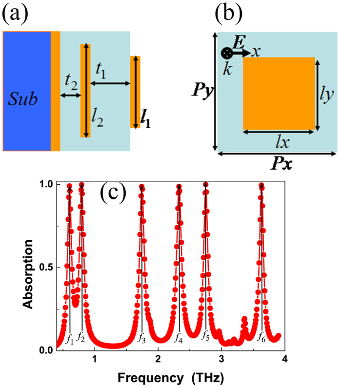
Figure 1(a) and (b) show the side- and top-view of the six-band MPA, respectively. As shown in Fig. 1(a), the presented six-band MPA is a dual-layer stacked resonance structure, and the length of the top metallic square patch (l1) is smaller than that of the bottom square patch (l2). Detailed parameters (in μm) of the six-band MPA are: l1 = l1x = l1y = 55, l2 = l2x = l2y = 65, t1 = 6, t2 = 4.5, P = Px = Py = 75. The calculation results of the whole paper are carried out using FDTD Solutions, which is based on finite-difference time-domain method. The other geometrical parameters of the presented MPA and the computational model as well as the appropriate boundary conditions applied in this paper are shown in the Section of the Methods.
Figure 1.
(a) and (b) show the side- and top-view of the six-band MPA, respectively, the parameters (in μm) of the MPA are: l1 = l1x = l1y = 55, l2 = l2x = l2y = 65, t1 = 6, t2 = 4.5, P = Px = Py = 75; (c) is the absorption spectrum of the designed six-band MPA.
Figure 1(c) presents the simulated absorption spectra of the designed six-band MPA. As you can seen in Fig. 1(c), six obvious absorption peaks or bands at frequencies of 0.60 THz (f1), 0.80 THz (f2), 1.74 THz (f3), 2.33 THz (f4), 2.75 THz (f5), and 3.63 THz (f6) with high absorption coefficients of 99.10%, 99.90%, 98.77%, 98.82%, 99.99%, and 99.63% are observed, respectively. The bandwidths (full width half maximum) of the six resonance peaks from low- to high-frequency are 0.079 THz, 0.088 THz, 0.097 THz, 0.097 THz, 0.079 THz, and 0.079 THz, respectively. The Q (the resonance frequency with respect to the bandwidth) values of the modes f1, f2, f3, f4, f5, and f6 are 7.59, 9.09, 17.94, 24.02, 34.81, and 45.95, respectively. Meanwhile, the off-resonances (for example at 0.70 THz, 1.32 THz, 2.10 THz, 2.50 THz, 3.20 THz, and 3.80 THz) absorption coefficients of presented MPA are quite low, not exceeding 30%. These resonance characteristics indicate that the six absorption bands are apparently discernible and the perfect absorption with quite narrow bandwidth merely appears near the operating frequency.
The resonance modes f1, f3, and f5 are the fundamental mode (i.e., the 1-order), 3-order, and 5-order responses of the metallic patch l2, respectively, while the modes f2, f4, and f6 are the 1-order, 3-order, and 5-order responses of the metallic patch l1, respectively. That is to say, the resonance modes of the f1, f3, f5 and f2, f4, f6 are the multiple-order responses of the metallic patches l2, and l1, respectively. Utilizing the classical antenna theory and LC resonance model, a further understand of the absorption mechanism of six-band MPA can be given54,55,56,57. This is a known fact that the operating frequency of the absorber satisfies the following form54,55,56,57:
 |
where c represents the light speed, n is the refractive index of the dielectric slab, l is the metallic pattern length, i, j = 0, 1, 2, … are integers. According to this equation, it is obvious that the operating frequency fij and the metallic pattern length l are inversely related. In particular, the operating frequencies of the 5-order (i = 5, j = 0) and 3-order (i = 3, j = 0) responses of the absorber should be about five and three times of the 1-order (i = 1, j = 0) response. In the six-band MPA, the frequencies of the modes f5 (2.75 THz) and f3 (1.74 THz) are about five and three times of the modes f1 (0.60 THz), respectively. The frequencies of modes f6 (3.63 THz) and f4 (2.33 THz) are about five and three times of the modes f2 (0.80 THz), respectively. Consequently, we can conclude that the resonance modes f1 (f2), f3 (f4), and f5 (f6) are indeed the 1-order, 3-order, and 5-order responses (or multiple-order responses) of the metallic patch l2 (l1), respectively. The slight frequency deviations are mainly derived from the interactions of these two metallic layers, see the field distributions in below Fig. 2.
Figure 2.
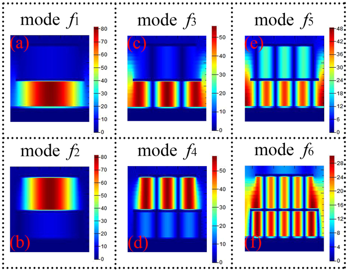
(a–f) are the magnetic field (|Hy|, in the plane of y = 0) distributions of the six-band MPA at modes f1, f2, f3, f4, f5, and f6, respectively.
The absorption mechanism (or physical origin) of the six-band MPA can be better gained by analyzing and investigating the distributions of the magnetic (|Hy|) fields in six different resonance modes. As shown in Fig. 2, it is obvious that the |Hy| distributions of the resonance modes f1, f2, f3, f4, f5, and f6 are primarily gathered in the dielectric layers of the six-band MPA. Thus, these resonance modes are all attributed to the localized EM responses of the MPA. In addition, we found that the field distributions of the modes f1, f3, and f5 are mainly focused on the dielectric layer t2, and the field distributions of modes f2, f4, and f6 are primarily gathered in the dielectric layer t1. These field distribution characteristics show that the modes f1, f3, and f5 are mainly associated with the excitation of the second metallic layer, while the modes f2, f4, and f6 are primarily the consequence of the excitation of the first metallic layer. To study the resonance mechanism of each resonance mode, we analyze the field distribution of each resonance mode in detail. The field distribution of the frequency at 0.60 THz (mode f1) is mainly distributed in the dielectric layer t2, while its field distribution at dielectric layer t1 is neglected, see Fig. 2(a). Besides, it is also found that there is only a resonance region (or a strong node) in the dielectric layer t2. Thus, the resonance mode f1 is the fundamental mode resonance (or 1-oder response) of the metallic patch l2. For resonance mode f2, its field distribution is primarily focused on the dielectric layer t1, see Fig. 2(b). We also observed that the field distribution of the mode f2 in dielectric layer t1 has only a strong node. As a result, the mode f2 is the 1-order response of the metallic patch l1. For resonance mode f3, three strong resonance regions are found in the dielectric layer t2, see Fig. 2(c). Similarly, three strong nodes are also observed in the dielectric layer t1 for resonance mode f4, see Fig. 2(d). Therefore, the resonance modes f3, and f4 are due to the 3-order response of the metallic patches l2, and l1, respectively. For resonance mode f5, see Fig. 2(e), its magnetic field is mainly gathered in the dielectric layer t2, while only a small part of magnetic field is observed in the dielectric layer t1. Besides, for field distribution of the resonance mode f5, it is noted that five strong nodes are found in the dielectric layer t2. Therefore, the resonance mode f5 is the 5-order response of the metallic patches l2. However, the field distribution of the mode f6 is different from the mode f5. As shown in Fig. 2(f), not only the dielectric layer t1 but also the dielectric layer t2 has strong field distributions for resonance mode f6. Notably, five strong resonance regions (or nodes) are found in both of the dielectric layers t1 and t2. Therefore, the resonance mode f6 is attributed to the hybridization (or coupling) of 5-order response of the metallic layers l1 and l2. Based on the combination of two sets of multiple-order responses (i.e., the 1-oder, 3-oder, and 5-order responses) of the two different sized metallic layers, six-band MPA is realized. The absorption mechanism of six-band MPA is different from previous multiple-band MPAs that only using the overlapping of the single resonance mode (in particular of the 1-order response) of metallic patterns27,28,29,34,35,36,37,38,39,40.
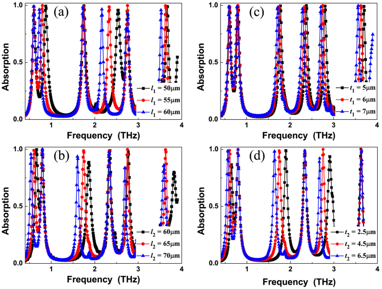
Because the resonance modes f1, f3, f5, and f2, f4, f6 are the multiple-order responses (1-order, 3-order, and 5-order resonances) of the metallic layer l2, and l1, respectively, the size change of the metallic layers will cause the shift of the frequencies in its corresponding resonance modes. As shown in Fig. 3(a), it is clear that the size change of l1 only affects the frequencies of the modes f2, f4, and f6, while the frequency changes of the modes f1, f3, and f5 are neglected. For change of the l2, see Fig. 3(b), the frequencies of the modes f1, f3, and f5 gradually decrease with the increase of the patch length l2. In addition, we also observed that the resonance frequency of the mode f6 has a large dependence on the change of the length l2. The results obtained in Fig. 3(a) and (b) are in agreement with the theoretical predictions. The adjustment or change of the resonance frequencies can also be obtained through varying the thicknesses of the dielectric layers t1, and t2. It can be seen from Fig. 3(c) that the change of the thickness t1 has a great influence on the resonance frequencies of the last four resonance modes (f3, f4, f5, and f6), while the frequency changes of the first two resonance modes are neglected. Moreover, for change of the thickness t2, see Fig. 3(d), it is found that its thickness change only influences the resonance frequencies of the modes f1, f3, and f5, while the frequencies of other resonance modes are nearly unchanged. Therefore, we can conclude that the size changes of the metallic layers and the thickness changes of the dielectric layers have the ability to adjust or shift the operating frequencies of the six-band MPA.
Figure 3.
(a) is the dependence of the absorption spectra on the length change of the l1 (then l2 = 65 μm, t1 = 6 μm, and t2 = 4.5 μm); (b) shows the dependence of the absorption on the change of the l2 (then l1 = 55 μm, t1 = 6 μm, and t2 = 4.5 μm); (c) shows the dependence of the absorption on the thickness change of the t1 (then l1 = 55 μm, l2 = 65 μm, and t2 = 4.5 μm); (d) is the dependence of the absorption on the change of the t2 (then l1 = 55 μm, l2 = 65 μm, and t1 = 6 μm).
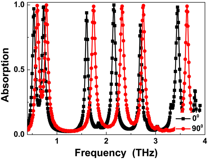
Due to four-fold symmetric of these two metallic square patches, the six-band MPA presented here is polarization insensitive to the incident EM waves. Although the polarization insensitive six-band MPA has great application prospects, the development of the polarization tunable six-band MPA in many areas (such as specific EM wave polarization detection) is necessary and useful. Based on the results obtained in Fig. 3(a) and (b), in this paragraph, a six-band polarization tunable MPA through varying the sizes of the metallic layers in two orthogonal polarization directions is demonstrated. The sizes (in μm) of the presented six-band polarization tunable MPA are: l1x = 60, l2x = 70, l1y = 55, l2y = 65. The other parameters of the polarization tunable MPA are the same as those in Fig. 1(a) and (b). As illustrated in Fig. 4, six clear resonance bands are achieved at frequencies of 0.53 THz, 0.73 THz, 1.60 THz, 2.15 THz, 2.69 THz, and 3.44 THz with the average absorptivities greater than 95.29% in the 0 degree of polarization (i.e., along the x-axis). Six different absorption peaks are also observed in the polarization angle of 90 degrees (parallel to the y-axis). However, the resonance frequencies of the six-band MPA in the 90 degrees of polarization shift to 0.60 THz, 0.79 THz, 1.74 THz, 2.32 THz, 2.75 THz, and 3.64 THz, respectively. The frequency changes of the six resonance modes in 0 and 90 degrees are due to the different metallic layer sizes in two perpendicular directions. The six-band polarization tunable MPA can be potentially used to detect the EM waves of specific polarization and even to control and manipulate the polarization angle of incident waves58,59.
Figure 4. Absorption spectra of the six-band polarization tunable MPA.
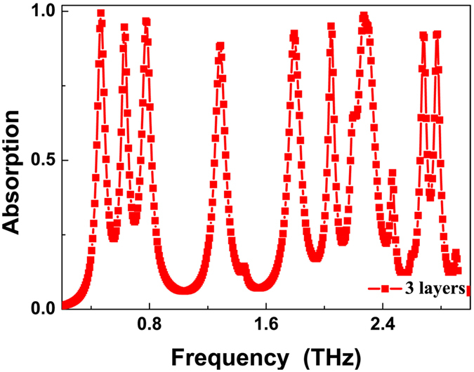
The number of the resonance absorption peaks can be further increased by stacking more metallic layers. We use the three-layer stacked structure as an example to investigate its resonance absorption peaks. The optimal sizes (in μm, from top layer to bottom layer) of the presented three-layer stacked resonance structure are: l1 = 55, l2 = 65, l3 = 80, t1 = 7.6, t2 = 5.0, t3 = 6.1, P = 95. The other geometric parameters, including the refractive index of the dielectric layer and the metallic layer conductivity are the same as used in six-band MPA. The resonance absorption of the designed three-layer stacked MPA is illustrated in Fig. 5. Nine distinct absorption bands are obtained at frequencies of 0.47 THz (f1), 0.63 THz (f2), 0.78 THz (f3), 1.28 THz (f4), 1.79 THz (f5), 2.05 THz (f6), 2.27 THz (f7), 2.68 THz (f8), and 2.78 THz (f9) with the absorption of 99.45%, 94.77%, 96.75%, 88.55%, 92.60%, 95.04%, 98.68%, 92.03%, and 92.06%, respectively. The bandwidths of these peaks from low- to high-frequency are 0.067 THz, 0.060 THz, 0.077 THz, 0.088 THz, 0.095 THz, 0.056 THz, 0.049 THz, and 0.049 THz, respectively, and the Q values of nine resonance bands are 7.01, 10.50, 10.13, 14.55, 18.84, 36.61, 12.61, 54.69, and 56.73, respectively.
Figure 5. Simulated absorption spectra of the presented nine-band MPA (or three-layer stacked resonance structure).
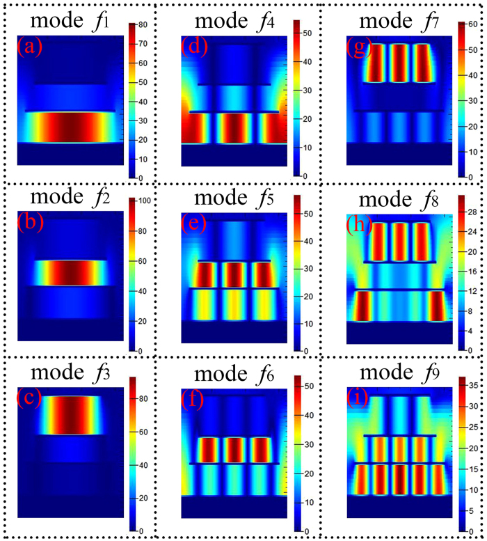
Furthermore, the distributions of the |Hy| fields are provided to reveal or gain the absorption mechanism of the nine-band MPA, as shown in Fig. 6. Based on the above discussions and the |Hy| field distributions of the different resonance modes in the nine-band MPA, we can conclude that the modes f1, f2, and f3 are the 1-order response of the metallic patches l3, l2, and l1, respectively, see Fig. 6(a–c). The resonance modes f4, and f7 are the 3-order response of the patches l3, and l1, respectively, see Fig. 6(d) and (g). The other resonance modes (f5, f6, f8, and f9) of the nine-band MPA are due to the hybridization of multiple-order responses of the metallic layers, see Fig. 6(e,f,h and i). For example, the resonance mode f5 originates from the hybridization (or coupling) of the 3-order responses of the metallic patches l2 and l3, see Fig. 6(e), and the mode f6 is derived from the coupling of the 3-order response of the metallic patch l2 and 5-order response of the metallic structure l3, see Fig. 6(f).
Figure 6.
(a–i) Show the magnetic field (|Hy|) distributions of the nine-band MPA at resonance modes f1, f2, f3, f4, f5, f6, f7, f8 and f9, respectively.
Conclusion
In conclusion, a six-band polarization insensitive terahertz MPA based on a dual-layer stacked resonance structure is numerically investigated and studied. Six resonance bands with absorption average greater than 99.37% are achieved. Each layer of the resonance structure corresponds to three absorption peaks (1-oder, 3-order, and 5-order responses), and thus the absorption mechanism of the six-band MPA is attributed to the combination of two sets of the three resonance modes (1-oder, 3-order, and 5-order responses) of the two metallic layers in the stacked structure. The field distributions of the six resonance bands are given to reveal or gain the absorption mechanism of the six-band MPA. Besides, the design also has the ability to tune or change the resonance frequencies of the six-band MPA through varying the sizes of the metallic layers or the thicknesses of the dielectric layers. Employing this results, a six-band polarization tunable MPA is also analyzed and demonstrated. Furthermore, the number of the resonance bands or peaks can be further increased by stacking more metallic square patches. As an example, we found that three-layer stacked resonance structure can achieve nine-band near-perfect absorption. Six-band and even nine-band MPAs obtained here can find potential applications in many optoelectronic related areas. Once the structure is fabricated, however, the absorption performance (including the resonance frequency and the absorption strength) of the absorber is unable to change. Some temperature-dependent materials, bias-tunable materials, and even microfluidic systems can be used to overcome this kind of shortcoming. The further works are the design of the active tunable multiple-band light absorbers.
Methods
Numerical modeling and detailed parameters of the presented MPA
The geometric parameters of the six-band MPA are shown in Fig. 1(a) and (b). Detailed parameters (in μm) of the six-band MPA are: l1 = l1x = l1y = 55, l2 = l2x = l2y = 65, t1 = 6, t2 = 4.5, P = Px = Py = 75. The metallic layers of the six-band MPA are made of Au, and the thickness and conductivity of them are 0.4 μm, and 4.09 × 10⁷ S/m, respectively. The refractive index of the dielectric layer is n = 3.2 + i0.025. In this investigation, we utilize normally incident EM waves with E field parallel to the x-axis as illustrated in Fig. 1(b). Periodic boundary conditions are employed along the direction of the wave propagating, and in the normal to the wave propagating direction, perfect matching layers are used. The frequency dependent absorption can be given by: A(w) = 1 − T(w) − R(w), where T(w) and R(w) are the frequency dependent transmission and reflection, respectively. T(w) is close to zero because of the presence of the metallic board. As a result, the A(w) can be obtained using A(w) = 1 − R(w). We can achieve perfect absorption (A(w) = 1) when the R(w) is completely suppressed (i.e., the impedance of the structure is equal to that of the air).
Additional Information
How to cite this article: Wang, B.-X. et al. Six-band terahertz metamaterial absorber based on the combination of multiple-order responses of metallic patches in a dual-layer stacked resonance structure. Sci. Rep. 7, 41373; doi: 10.1038/srep41373 (2017).
Publisher's note: Springer Nature remains neutral with regard to jurisdictional claims in published maps and institutional affiliations.
Acknowledgments
This work was supported by the National Natural Science Foundation of China (Grant No. 11647143), Natural Science Foundation of Jiangsu Province (Grant No. BK20160189), Jiangsu Provincial Research Center of Light Industrial Optoelectronic Engineering and Technology (Grant No. BM2014402), and the Fundamental Research Funds for the Central Universities (Grant No. JUSRP115A13).
Footnotes
Author Contributions B.X.W. conceived the research, conducted simulations and analysis, wrote the manuscript; G.Z.W., T.S, and L.L.W. provided some useful suggestions.
References
- Zheludev N. I. & Plum E. Reconfigurable nanomechanical photonic metamaterials. Nat. Nanotechnol. 11, 16–22 (2016). [DOI] [PubMed] [Google Scholar]
- Grant J., Mccrindle I. J. H. & Cumming D. R. S. Multi-spectral materials: Hybridisation of optical plasmonic filters, a mid infrared metamaterial absorber and a terahertz metamaterial absorber. Opt. Express 24, 3451–3463 (2016). [DOI] [PubMed] [Google Scholar]
- Landy N. I., Sajuyigbe S., Mock J. J., Smith D. R. & Padilla W. J. Perfect metamaterial absorber. Phys. Rev. Lett. 100, 207402 (2008). [DOI] [PubMed] [Google Scholar]
- Samson Z. L. et al. Metamaterial electro-optic switch of nanoscale thickness. Appl. Phys. Lett. 96, 143105 (2010). [Google Scholar]
- Kaschke J. et al. A helical metamaterial for broadband circular polarization conversion. Adv. Opt. Mater. 3, 1411–1417 (2015). [Google Scholar]
- Li H. M. et al. Low-loss metamaterial electromagnetically induced transparency based on electric toroidal dipolar response. Appl. Phys. Lett. 106, 083511 (2015). [Google Scholar]
- He J., Ding P., Wang J., Fan C. & Liang E. Ultra-narrow band perfect absorbers based on plasmonic analog of electromagnetically induced absorption. Opt. Express 23, 6083–6091 (2015). [DOI] [PubMed] [Google Scholar]
- Watts C. M., Liu X. & Padilla W. J. Metamaterial electromagnetic wave absorbers. Adv. Mater. 24, OP98–OP120 (2012). [DOI] [PubMed] [Google Scholar]
- Cui Y. et al. Plasmonic and metamaterial structures as electromagnetic absorbers. Laser Photon. Rev. 8, 495–520 (2014). [Google Scholar]
- Tao H. Padilla W. J., Zhang X. & Averitt R. D. Recent progress in electromagnetic metamaterial devices for terahertz applications. IEEE J. Sel. Top. Quant. 17, 92–101 (2011). [Google Scholar]
- Liu X., Starr T., Starr A. F. & Padilla W. J. Infrared spatial and frequency selective metamaterial with near-unity absorbance. Phys. Rev. Lett. 104, 207403 (2010). [DOI] [PubMed] [Google Scholar]
- Cong L. et al. Experimental demonstration of ultrasensitive sensing with terahertz metamaterial absorbers: A comparison with the metasurfaces. Appl. Phys. Lett. 106, 031107 (2015). [Google Scholar]
- Chen W. C. et al. Role of surface electromagnetic waves in metamaterial absorbers. Opt. Express 24, 6783–6792 (2016). [DOI] [PubMed] [Google Scholar]
- Ogawa S. et al. Mushroom plasmonic metamaterial infrared absorbers. Appl. Phys. Lett. 106, 041105 (2015). [Google Scholar]
- Ghosh S. & Srivastava K. V. An equivalent circuit model of FSS-based metamaterial absorber using coupled line theory. IEEE Antennas Wireless Propag. Lett. 14, 511–514 (2015). [Google Scholar]
- Li Z., Butun S. & Aydin K. large-area, lithography-free super absorbers and color filters at visible frequencies using ultrathin metallic films. ACS Photon. 2, 183–188 (2015). [Google Scholar]
- Wang B. X., Zhai X., Wang G. Z., Huang W. Q. & Wang L. L. Frequency tunable metamaterial absorber at deep-subwavelength scale. Opt. Mater. Express 5, 227–235 (2015). [Google Scholar]
- Walter R. et al. Large-area low-cost tunable plasmonic perfect absorber in the near infrared by colloidal etching lithography. Adv. Opt. Mater. 3, 398–403 (2015). [Google Scholar]
- Akselrod G. M. et al. Large-area metasurface perfect absorbers from visible to near-infrared. Adv. Mater. 27, 8028–8034 (2015). [DOI] [PubMed] [Google Scholar]
- Chen H. T. Interference theory of metamaterial perfect absorbers. Opt. Express 20, 7165–7172 (2012). [DOI] [PubMed] [Google Scholar]
- Liu N., Mesch M., Weiss T., Hentschel M. & Giessen H. Infrared perfect absorber and its application as plasmoinc sensor. Nano Lett. 10, 2342–2348 (2010). [DOI] [PubMed] [Google Scholar]
- Hao J. et al. High performance optical absorber based on a plasmonic metamaterial. Appl. Phys. Lett. 96, 251104 (2010). [Google Scholar]
- Shchegolkov D. Y., Azad A. K., Ohara J. F. & Simakov E. I. Perfect subwavelength fishnetlike metamaterial-based film terahertz absorbers. Phys Rev. B 82, 205117 (2010). [Google Scholar]
- Hokmabadi M. P., Wilbert D. S., Kung P. & Kim S. M. Design and analysis of perfect terahertz metamaterial absorber by a novel dynamic circuit model. Opt. Express 21, 16455–16465 (2013). [DOI] [PubMed] [Google Scholar]
- Wilbert D. S., Hokmabadi M. P., Kung P. & Kim S. M. Equivalent-circuit interpretation of the polarization insensitive performance of THz metamaterial absorbers. IEEE Trans. THz Sci Techn. 3, 846–850 (2013). [Google Scholar]
- Hokmabadi M. P., Wilbert D. S., Kung P. & Kim S. M. Polarization-dependent, frequency-selective THz stereometamaterial perfect absorber. Phys. Rev. Appl. 1, 044003 (2014). [Google Scholar]
- Wen Q. Y. et al. Dual band terahertz metamaterial absorber: Design, fabrication, and characterization. Appl. Phys. Lett. 95, 241111 (2009). [Google Scholar]
- Tao H. et al. A dual band terahertz metamaterial absorber. J. Phys. D 43, 225102 (2010). [Google Scholar]
- MA Y. et al. A terahertz polarization insensitive dual band metamaterial absorber. Opt. Lett. 36, 945–947 (2011). [DOI] [PubMed] [Google Scholar]
- Bhattacharyya S. Ghosh S., Chaurasiya D. & Srivastava K. V. Bandwidth-enhanced dual-band dual-layer polarization-independent ultra-thin metamaterial absorber. Appl. Phys. A 118, 207–215 (2015). [Google Scholar]
- Wang B. X., Zhai X., Wang G. Z., Huang W. Q. & Wang L. L. A novel dual-band terahertz metamaterial absorber for a sensor application. J. Appl. Phys. 117, 014504 (2015). [Google Scholar]
- Bai Y., Zhao L., Ju D., Jiang Y. & Liu L. Wide-angle, polarization-independent and dual-band infrared perfect absorber based on L-shaped metamaterial. Opt. Express 23, 8670–8680 (2015). [DOI] [PubMed] [Google Scholar]
- Yao G. et al. Dual-band tunable perfect metamaterial absorber in the terahertz range. Opt. Express 24, 1518–1527 (2016). [DOI] [PubMed] [Google Scholar]
- Zhang Y. et al. Independently tunable dual-band perfect absorber based on graphene at mid-infrared frequencies. Sci. Rep., 5, 18463 (2015). [DOI] [PMC free article] [PubMed] [Google Scholar]
- Shen X. et al. Polarization-independent wide-angle triple-band metamaterial absorber. Opt. Express 19, 9401–9407 (2011). [DOI] [PubMed] [Google Scholar]
- Li H. et al. Ultrathin multiband gigahertz metamaterial absorbers. J. App. Phys. 110, 014909 (2011). [Google Scholar]
- Zhang B., Hendrickson J. & Guo J. Multispectral near-near metamaterial absorbers using spatially multiplexed palsmon resonance metal square structures. J. Opt. Soc. Am. B 30, 656–662 (2013). [Google Scholar]
- Park J. W. et al. Multi-band metamaterial absorber based on the arrangement of donut-type resonators. Opt. Express 21, 9691–9702 (2013). [DOI] [PubMed] [Google Scholar]
- Bhattacharyya S. & Srivastava K. V. Triple band polarization-independent ultra-thin metamaterial absorber using electric field-driven LC resonator. J. Appl. Phys. 115, 064508 (2014). [Google Scholar]
- Zhai H., Zhan C., Li Z. & Liang C. A triple-band ultrathin metamaterial absorber with wide-angle and polarization stability. IEEE Antennas Wireless Propag. Lett. 14, 241–244 (2015). [Google Scholar]
- Kajtar G. Kafesaki M., Economoou E. N. & Soukoulis C. M. Theoretical model of homogeneous metal-insulator-metal perfect multi-band absorbsrs for the visible spectrum. J. Phys. D 49, 055104 (2016). [Google Scholar]
- Chen J., Hu Z., Wang S., Huang X. & Liu M. A triple-band, polarization- and incident angle-independent microwave metamaterial absorber with interference theory. Eur. Phys. J. B 89, 14 (2016). [Google Scholar]
- Agarwal M., Behera A. K. & Meshram M. K. Wide-angle quad-band polarisation-insensitive metamaterial absorber. Electron. Lett. 52, 340–342 (2016). [Google Scholar]
- Wang G. D. et al. Multi-band microwave metamaterial absorber based on coplanar Jerusalem crosses. Chin. Phys. B 23, 017802 (2014). [Google Scholar]
- Xu Z. C., Gao R. M., Ding C. F., Zhang Y. T. & Yao J. Q. Multiband metamaterial absorber at terahertz frequencies. Chin. Phys. Lett. 31, 054205 (2014). [Google Scholar]
- Hu F. et al. Design of a polarization insensitive multiband terahertz metamaterial absorber. J. Phys. D. 46, 195103 (2013). [Google Scholar]
- Chaurasiya D., Ghosh S., Bhattacharyya S. & Srivastava K. V. An ultrathin quad-band polarization-insensitive wide-angle metamaterial absorber. Microw. Opt. Techn. Lett. 57, 697–702 (2015). [Google Scholar]
- Zheng D., Cheng Y., Cheng D., Nie Y. & Gong R. Z. Four-band polarization-insensitive metamaterial absorber based on flower-shaped structures. Prog. Electromagn. Res. 142, 221–229 (2013). [Google Scholar]
- Viet D. T. et al. Perfect absorber metamaterials: Peak, multi-band and broadband absorption. Opt. Commun., 322, 209–213 (2014). [Google Scholar]
- Wang B. X., Zhai X., Wang G. Z., Huang W. Q. & Wang. L. L. Design of a four-band and polarization-insensitive terahertz metamaterial absorber. IEEE Photon. J. 7, 4600108 (2015). [Google Scholar]
- Liu S. et al. A bi-layered quad-band metamaterial absorber at terahertz frequencies. J. Appl. Phys. 118, 245304 (2015). [Google Scholar]
- Xiao D. & Tao K. Ultra-compact metamaterial absorber for multiband light absorption at mid-infrared frequencies. Appl. Phys. Express 8, 102001 (2015). [Google Scholar]
- Wang W. et al. Ultra-thin quadri-band metamaterial absorber based on spiral structure. Appl. Phys. A 118, 443–447 (2015). [Google Scholar]
- Balanis C. A. Antenna theory: Analysis and designs, Chap.6 (Wiley, Hoboken, New Jersey, 2005). [Google Scholar]
- Peng X. Y., Wang B., Lai S., Zhang D. H. & Teng J. H. Ultrathin multi-band planar metamaterial absorber based on standing wave resonances. Opt. Express 20, 27756–27765 (2012). [DOI] [PubMed] [Google Scholar]
- Sellier A., Teperik T. V. & Lustrac A. D. Resonant circuit model for efficient metamaterial absorber. Opt. Express 21, A997–A1006 (2013). [DOI] [PubMed] [Google Scholar]
- Wang B. X. Single-patterned metamaterial structure enabling multi-band pefect absorption. Plasmonic (2016). doi: 10.1007/s11468-016-0234-1. [DOI] [Google Scholar]
- Wang B. X., Wang G. Z., Zhai X. & Wang L. L. Polarization tunable terahertz metamaterial absorber. IEEE Photon. J. 7, 4600507 (2015). [Google Scholar]
- Grant J., Ma Y., Saha S., Khalid A. & Cumming D. R. S. Polarization insensitive, broadband terahertz metamaterial absorber. Opt. Lett. 36, 3476–3478 (2011). [DOI] [PubMed] [Google Scholar]


