Abstract
GaAs photovoltaics are promising candidates for indoor energy harvesting to power small-scale (≈1 mm2) electronics. This application has stringent requirements on dark current, recombination, and shunt leakage paths due to low-light conditions and small device dimensions. The power conversion efficiency and the limiting mechanisms in GaAs photovoltaic cells under indoor lighting conditions are studied experimentally. Voltage is limited by generation–recombination dark current attributed to perimeter sidewall surface recombination based on the measurements of variable cell area. Bulk and perimeter recombination coefficients of 1.464 pA/mm2 and 0.2816 pA/mm, respectively, were extracted from dark current measurements. Resulting power conversion efficiency is strongly dependent on cell area, where current GaAs of 1-mm2 indoor photovoltaic cells demonstrates power conversion efficiency of approximately 19% at 580 lx of white LED illumination. Reductions in both bulk and perimeter sidewall recombination are required to increase maximum efficiency (while maintaining small cell area near 1 mm2) to approach the theoretical power conversion efficiency of 40% for GaAs cells under typical indoor lighting conditions.
Index Terms: Compound semiconductors, diodes, electronic devices, recombination
I. Introduction
Indoor energy harvesting for small-scale (≈1 mm2) sensors has recently generated considerable attention due to the development of pervasive sensing and the Internet of Things. In contrast to solar photovoltaics, indoor lighting conditions have much lower light levels and smaller area cells, where dark current, shunt current leakage paths, and cell edge effects are critical in determining power conversion efficiency. The III–V solar cells have demonstrated excellent performance under indoor lighting conditions [1], [2] due to their high quantum efficiency, near match of the bandgap energy to the indoor lighting spectrum, and large shunt resistance. Theoretical calculations have suggested a maximum power conversion efficiency of up to 60% under indoor lighting conditions [1], [3], [4]. A power conversion efficiency of 21% was obtained using an Al0.2Ga0.8As photovoltaic cell under indoor lighting conditions [1]. Efficient indoor energy harvesting has also been reported for larger (≈1 cm2) perovskite photovoltaics [5], though scaling to smaller geometries and device lifetime stability are still unknown. GaAs and related III–V compounds, such as AlGaAs, show great promise with demonstrated conversion efficiency of >20%, which is large enough for perpetual operation of millimeter-scale systems, but is still at least a factor of 2 below the calculated theoretical maximum efficiency [1]. Improvements in cell efficiency can achieve critical objectives in reducing system size, functionality, and frequency of tasks. Accordingly, this paper seeks to identify and quantify limiting mechanisms in small-area GaAs photovoltaic cells operating under low-light conditions.
Improving the power conversion efficiency of GaAs-based indoor photovoltaics requires a deeper understanding of limiting loss mechanisms. Primary loss mechanisms for photovoltaics are transparency, thermalization, optical, recombination, and resistive losses. Since the spectrum of indoor lighting is narrow and limited to photons with energy greater than the bandgap of GaAs, there are no transparency losses in indoor photovoltaics, in contrast to the conventional solar cells. Thermalization losses occur from fast thermal relaxation of carriers following photogeneration at energies above the bandgap energy, a fundamental loss mechanism for a single-junction diode, which is less severe under the narrowband indoor conditions in comparison with the broadband solar spectrum. Optical losses result from incomplete transfer of incident photons to the active area, including reflection from metal contacts and the incident surface. Recombination losses result from the annihilation of photogenerated electron–hole pairs prior to carrier collection. Under low-flux conditions, such as indoor lighting, recombination losses can become dominant in determining the conversion efficiency of a photovoltaic cell. Recombination can occur in the bulk, surface, or perimeter of the device, where the latter factors become highly significant as cell area decreases. The influence of perimeter recombination on the performance degradation of GaAs-based diodes and solar cells has been documented previously [6]–[12]. Losses resulting from contact and series resistances are typically insignificant for indoor photovoltaics under low-flux, and subsequently low current density, conditions. Shunt conductance, however, may result in substantial performance degradation for small cells under low-flux conditions, particularly at the device perimeter. In this paper, the performance limitations of small-area GaAs photovoltaic cells under low-flux indoor lighting conditions are investigated.
II. Experiment and Results
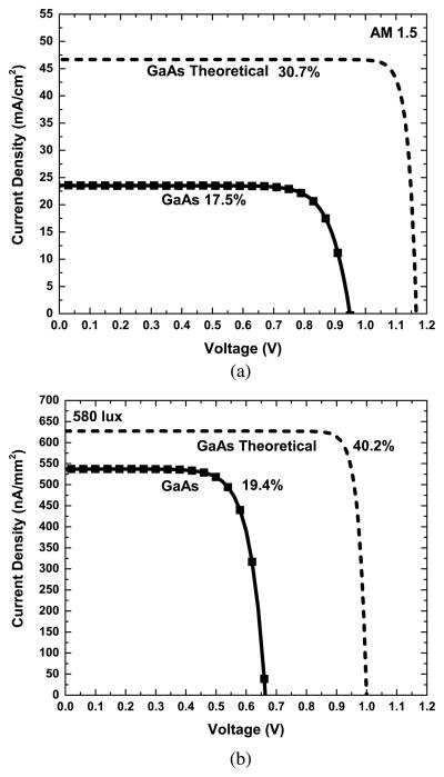
GaAs photovoltaic cells were fabricated with variable area, where device structure shown in Table I and fabrication details were published previously [1]. A layer of Si3N4 was deposited on the top surface to serve as both an antireflection coating and sidewall passivation layer. Cell area ranged from 0.022 to 0.172 mm2, with corresponding perimeter/area (P/A) ratios from 29.1 to 10.4 mm−1. Current–voltage characteristics were measured under dark conditions and variable illumination using a Keithley 4200 Semiconductor Characterization System with preamplifier to provide current measurements with femtoamp resolution. Example measured current–voltage curves and comparison with theoretical limits are shown in Fig. 1 for illumination under [Fig. 1(a)] simulated AM1.5 illumination and [Fig. 1(b)] white light LED illumination. The accuracy of the optical source conditions corresponds to approximately 1 lx. The power conversion efficiency at the maximum power point is shown in Fig. 1, with the measurement accuracy of 0.1% limited by the accuracy of the optical illumination conditions. External quantum efficiency (EQE) of the cells over the white light LED spectral range was measured using a broadband quartz tungsten halogen lamp, monochromator, lock-in amplifier, and calibrated photodetector. The EQE measurements were used to examine short-circuit current and comparison with theoretical values. Current–voltage measurements for diodes with variable area were measured and analyzed to examine the impact of perimeter versus bulk recombination and shunt paths. The variable-area current–voltage measurements served to determine the sources of degradation in open-circuit voltage.
TABLE I.
GaAs Device Structure Under Study
| Type | Material | Thickness (nm) | Doping (cm−3) |
|---|---|---|---|
| p++ | GaAs | 200 | 2 × 10¹⁹ |
| p+ | Al0.8Ga0.2As | 30 | 2 × 10¹⁸ |
| p+ | GaAs | 250 | 6 × 10¹⁸ |
| n− | GaAs | 50 | 1 × 10¹⁸ |
| n− | GaAs | 100 | graded |
| n | GaAs | 550 | 5 × 10¹⁷ |
| n+ | Al0.3Ga0.7As | 150 | 1 × 10¹⁷ |
| n+ | GaAs | 300 | 2 × 10¹⁸ |
Fig. 1.
Measured and theoretical current density versus voltage curves of a 1-mm2 GaAs cell under (a) AM1.5 illumination and (b) white LED illumination. Corresponding power conversion efficiencies are labeled for the maximum power point.
A. External Quantum Efficiency
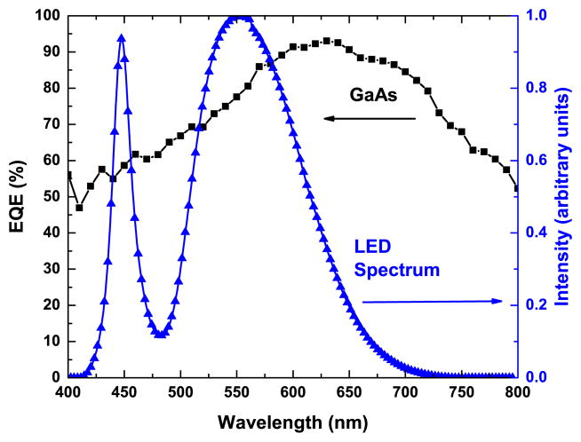
The EQE of a photovoltaic cell provides an indication of the effectiveness of the cell in absorbing incoming photons and collecting the photogenerated carriers. The measured EQE of the GaAs photovoltaic cell is shown in Fig. 2, along with the spectral content of the white light LED used in this paper to represent typical indoor lighting conditions with response in the range of 425–700 nm. Response is strong over the wavelengths of interest for the GaAs cell, where short-circuit current values are in agreement with EQE spectra shown in Fig. 2 [1]. In contrast to solar photovoltaics, problems associated with rear surface recombination and reduced absorption at longer wavelengths do not manifest themselves in the performance of indoor photovoltaics due to the narrow spectral band in the visible region. The cell demonstrates a drop in EQE at short wavelengths, and may be due to front surface recombination, emitter thickness and doping, and response of antireflection coating. The EQE results explain the decrease in measured short-circuit current in comparison with the theoretical values.
Fig. 2.
Measured EQE of GaAs cell along with the spectral content of the white LED used for indoor measurements.
B. Dark Current
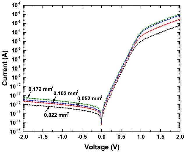
Dark current measurements under reverse and forward bias are shown in Fig. 3. In order to extract the diode parameters, a detailed analysis of diode behavior under forward bias is required. The diodes under forward bias exhibit a clear exponential behavior (linear on the semilog plot of Fig. 3) until approximately 0.8 V, and a series-resistance limited behavior at higher voltage. The exponential region of forward bias (up to 0.8 V) may be fit to the diode equation
Fig. 3.
Dark current measurements of GaAs cells of varying dimensions from which the diode parameters were extracted.
| (1) |
where J is the current density, J0 is the reverse saturation current density, q is the elementary charge, V is the voltage, n is the diode ideality factor, k is Boltzmann’s constant, and T is the temperature of the diode. The extracted parameters J0 and n are summarized in Table II, where reverse saturation current density ranges from 3.14 to 7.47 pA/mm2 with a strong P/A dependence. The diode ideality factor is near n = 2 for all cell geometries, indicating nonradiative recombination in the space charge region.
TABLE II.
Extracted Parameters Using (1)
| P/A (mm−1) | P (mm) | A (mm2) | J0 (pA/mm2) | n |
|---|---|---|---|---|
| 10.4 | 1.79 | 0.172 | 3.14 | 1.95 |
| 13.6 | 1.39 | 0.102 | 3.65 | 1.94 |
| 18.9 | 0.99 | 0.052 | 4.98 | 1.95 |
| 29.1 | 0.65 | 0.022 | 7.47 | 1.96 |
Further information can be extracted from the forward bias curve by fitting the curves to the expansion of (1)
| (2) |
where J01 and J02 represent the reverse saturation current densities for recombination in the quasi-neutral region and Shockley–Read–Hall recombination in the space charge region, respectively. The extracted parameters J01 and J02 are summarized in Table III for the GaAs cells of varying dimensions.
TABLE III.
Extracted Parameters Using (2)
| P/A (mm−1) | J01 (pA/mm2) | J02 (pA/mm2) |
|---|---|---|
| 10.4 | 2.85×10⁻⁷ | 4.30 |
| 13.6 | 4.18×10⁻⁷ | 5.30 |
| 18.9 | 4.79×10⁻⁷ | 6.94 |
| 29.1 | 4.49×10⁻⁷ | 9.58 |
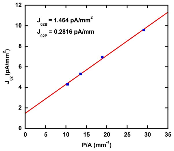
Extracted values of J02 exhibit a strong P/A dependence, as shown in Fig. 4. The reverse saturation current density J02 can be written as [9], [10]
Fig. 4.
Extracted saturation current versus P/A for GaAs cells of varying dimensions.
| (3) |
where J02B is the bulk recombination current density and is the perimeter recombination coefficient. The extracted values from Fig. 4 are J02B = 1.46 pA/mm2 and , similar to prior reports for high-efficiency GaAs solar cells [9], [10]. The perimeter recombination coefficient can be written as
| (4) |
where ni is the intrinsic carrier concentration, S0 is the surface recombination velocity, and Ls is the effective surface diffusion length. The product S0 Ls for these devices is determined to be 8.38 cm2/s, where high-efficiency GaAs solar cells have reported S0 Ls < 1 cm2/s [9], [10]. Further studies to passivate perimeter recombination will be critical in improving the performance of GaAs-based photovoltaic for low-flux and small-area applications, including the consideration of sidewall crystalline orientation [9].
C. Shunt Resistance
Parasitic shunt conductance can degrade cell performance, and becomes increasingly important under low-flux conditions, where short-circuit current values are small. The parasitic resistance components for a photovoltaic are described by
| (5) |
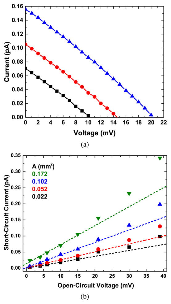
where Rs and Rsh are the series and shunt resistances, respectively. Shunt resistance values may be obtained from current–voltage measurements under extremely dim illumination, where JSC and VOC exhibit a near linear relationship when shunt conductance is dominant. This technique was developed by Chan and Phang [13] and has been used to directly measure the shunt resistance of a solar cell without the prior knowledge of solar cell parameters [13]–[15]. It should be noted that this technique does not require accurate knowledge of the source intensity, but rather measurements under variable light intensity where shunt resistance is dominant. Neglecting series resistance, JSC and VOC, may be related by [13]
| (6) |
Under dim conditions, the JSC term on the left side of (6) becomes dominant, resulting in the linear relation
| (7) |
Measured J–V relations for a select GaAs device under variable dim, <10 lx, lighting conditions are shown in Fig. 5(a), exhibiting a linear behavior. Resulting relationships for JSC and VOC under variable intensity, and for variable cell area, are shown in Fig. 5(b). The slope of the curves in Fig. 5(b) provides the values for Rsh, with the results shown in Table IV. Similar to the reverse saturation current density, the shunt resistance demonstrated a strong P/A dependence. Series resistance was examined for voltages >1 V. While the J–V relations are nonlinear in this range, a series resistance on the order of 0.1 Ω-cm2 is estimated, which is sufficiently low to not have an impact on the devices under the current and voltage range of interest for indoor energy harvesting.
Fig. 5.
Measured (a) current density versus voltage of a 0.172-mm2 GaAs cell under varying levels of extremely dim light and (b) short-circuit current versus open-circuit voltage of GaAs cells of varying dimensions under extremely dim conditions from which shunt resistance values were extracted.
TABLE IV.
Extracted Parasitic Resistance
| P/A (mm−1) | A (mm2) | Rsh (MΩ-cm2) |
|---|---|---|
| 10.4 | 0.172 | 27 |
| 13.6 | 0.102 | 23 |
| 18.9 | 0.052 | 16 |
| 29.1 | 0.022 | 5 |
III. Discussion
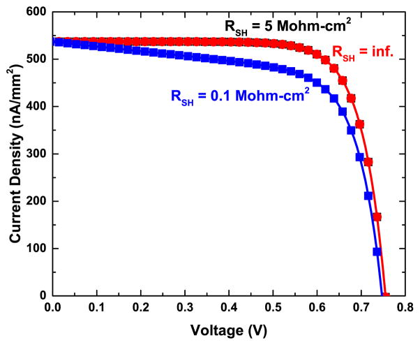
The dark current of the GaAs photovoltaic cells on the millimeter-scale is dominated by n = 2 perimeter recombination, where J0 has a strong P/A dependence ranging from 3.14 to 7.47 pA/mm2. These dark current levels have a strong influence on VOC at low illumination conditions (including typical indoor lighting illuminance). Shunt resistance also demonstrated a strong P/A dependence ranging from 5 to 27 MΩ-cm2. In order to study the effects of these shunt resistance levels on VOC, the photovoltaic response under indoor illumination conditions of a GaAs cell with P/A of 29.1 mm−1 and J0 of 7.47 pA/mm2 was simulated assuming infinite shunt resistance and 5-MΩ-cm2 shunt resistance (Fig. 6). It is clear from the simulations that the shunt resistance levels on the order of MΩ-cm2 are large enough to prevent shunt conductance under this indoor illumination condition, where degradation begins to appear at approximately 0.1 MΩ-cm2.
Fig. 6.
Calculated photovoltaic response under 580-lx white LED illumination for three GaAs cells, with infinite, 5-MΩ-cm2, and 0.1 MΩ-cm2 shunt resistance.
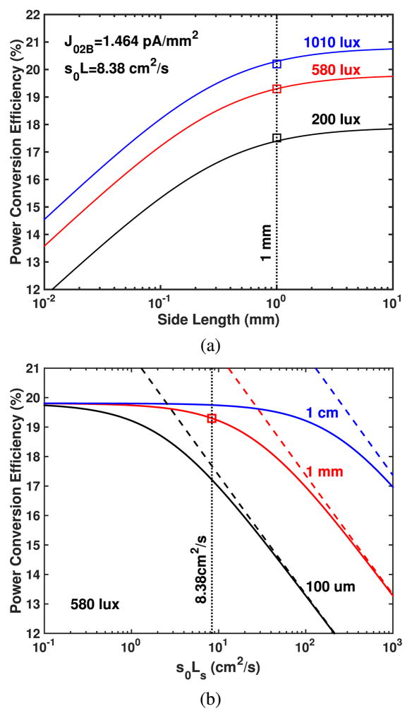
Dim lighting conditions (including indoor lighting conditions) magnify the effects of perimeter recombination, since the photocurrent is of the order of the n = 2 dark current. The calculated dependence of power conversion efficiency versus cell dimension is shown in Fig. 7(a), assuming J02B = 1.464 pA/mm2, S0 Ls = 8.38 cm2/s, and worst case parasitic resistance values of Rsh: 5 MΩ-cm2 and Rs : 150 mΩ-cm2. Calculated values for power conversion efficiency are determined at the maximum power point of the current–voltage relations given in (2)–(4). Measured power conversion efficiency for a 1-mm2 cell under the variable illumination conditions is shown in Fig. 7(a), agreeing with the calculated values. Power conversion efficiency could not be accurately determined with our experimental setup for smaller cells due to the challenges associated with determining optical illuminance for cells with dimensions approaching the contact pad area and predominance of optical shadowing effects. From the illumination range in Fig. 7(a), typical of indoor lighting, it is clear that the power conversion efficiency degrades for the cells with an area below 1 cm2, and quite dramatically for cells with an area decreasing below 1 mm2. The plateau achieved near 1 cm2 is limited by the bulk recombination mechanism described by J02B. The dramatic decrease in power conversion efficiency below 1 mm2 arises from perimeter sidewall recombination . This result highlights the importance of perimeter recombination for small-area cells under low-flux conditions, which may often be neglected for larger cells under typical solar irradiation.
Fig. 7.
Calculated power conversion efficiency for square GaAs cells with (a) varying side length and three different illumination conditions assuming experimental values from dark current measurements defined in the inset and (b) varying S0 Ls for three different side lengths assuming J02B = 1.464 pA/mm2 (solid lines) and 14.64 fA/mm2 (dashed lines). Experimentally measured values for 1-mm cells are plotted using square symbols.
The impact of perimeter recombination is shown in Fig. 7(b), illustrating the dependence on S0 Ls according to (4) and a fixed 1-mm2 cell area under typical indoor lighting conditions (580 lx). Experimentally measured data for a 1-mm2 cell is also shown and placed at the extracted value of S0 Ls = 8.38 cm2/s. The representation in Fig. 7(b) further illustrates that the present values for perimeter sidewall recombination achieved via Si3N4 passivation are borderline sufficient for maintaining power conversion efficiency of photovoltaic cells down to approximately 1 mm2. Further reduction in cell area will require substantial improvements in perimeter sidewall passivation. The plateau in power conversion efficiency near 20% at lower values of S0 Ls and larger cell area is again limited by bulk recombination represented by J02B. Further improvements in cell design, top/bottom surface passivation, and material quality may serve to reduce J02B and shift the efficiency plateaus in Fig. 7(a) and (b) upward. These improvements would further intensify the need to minimize perimeter surface recombination in order to realize maximum cell efficiency. For example, a decrease in J02B by a factor of 100 would result in the dashed-dotted lines shown in Fig. 7(b). While the plateau in efficiency is beyond the graph scale (not shown to preserve the range of interest in this paper), the maximum is approximately 28% with the requirement of approximately S0 Ls = 8.38 cm2/s to achieve this efficiency for a 1-mm2 cell. Chemical studies have shown improvements in the passivation of GaAs surface recombination using sulfides and thiols [16]–[19]. While such techniques have typically been employed in solar cells to boost open-circuit voltage and overall efficiency, they can similarly offer a path for dramatic improvements for small-area cells operating under low-flux conditions.
IV. Conclusion
GaAs photovoltaic cells demonstrate high EQE and power conversion efficiency over the indoor lighting spectrum. Shunt resistance values have been extracted from extremely dim current–voltage measurements and have been shown to be large and not a limiting factor in determining power conversion efficiency under typical indoor lighting conditions. The cells exhibit a diode ideality factor of n = 2 resulting from perimeter surface recombination current. Dark perimeter surface recombination is identified as the major source of VOC and efficiency degradation under typical indoor lighting conditions and for device areas at 1 mm2 and below. Further improvements in power conversion efficiency will require a decrease in bulk n = 2 recombination to raise the efficiency plateau, while placing greater demand on perimeter sidewall passivation to maintain conversion efficiency for device areas near 1 mm2 and below.
Acknowledgments
Research reported in this publication was supported by the National Science Foundation and the National Institutes of Health under Award R01CA195655.
Footnotes
The content is solely the responsibility of the authors and does not necessarily represent the official views of the National Science Foundation or National Institutes of Health.
References
- 1.Teran AS, et al. AlGaAs photovoltaics for indoor energy harvesting in mm-scale wireless sensor nodes. IEEE Trans Electron Devices. 2015 Jul;62(7):2170–2175. [Google Scholar]
- 2.Mathews I, King PJ, Stafford F, Frizzell R. Performance of III–V solar cells as indoor light energy harvesters. IEEE J Photovolt. 2016 Jan;6(1):230–235. [Google Scholar]
- 3.Freunek M, Freunek M, Reindl LM. Maximum efficiencies of indoor photovoltaic devices. IEEE J Photovolt. 2013 Jan;3(1):59–64. [Google Scholar]
- 4.Müller MF. Solar Cell Nanotechnology. Beverly, MA, USA: Scrivener Publishing; 2014. Indoor photovoltaics: Efficiencies, measurements and design; pp. 203–222. [Google Scholar]
- 5.Chen CY, Chang JH, Chiang KM, Lin HL, Hsiao SY, Lin HW. Perovskite photovoltaics for dim-light applications. Adv Funct Mater. 2015;25(45):7064–7070. [Google Scholar]
- 6.Henry CH, Logan RA. Effect of interface recombination at Alx Ga1−x As p–n junction perimeters on photoluminescence and current. J Vac Sci Technol. 1978;15(4):1471–1474. [Google Scholar]
- 7.Casey HC, Cho AY, Foy PW. Reduction of surface recombination current in GaAs p-n junctions. Appl Phys Lett. 1979;34(9):594–596. [Google Scholar]
- 8.DeMoulin PD, Tobin SP, Lundstrom MS, Carpenter MS, Melloch MR. Influence of perimeter recombination on high-efficiency GaAs p/n heteroface solar cells. IEEE Electron Device Lett. 1988 Aug;9(8):368–370. [Google Scholar]
- 9.Stellwag TB, Melloch MR, Lundstrom MS, Carpenter MS, Pierret RF. Orientation-dependent perimeter recombination in GaAs diodes. Appl Phys Lett. 1990;56(17):1658–1660. [Google Scholar]
- 10.Stellwag TB, et al. Effects of perimeter recombination on GaAs-based solar cells. Proc. 21st IEEE Photovolt. Specialists Conf; 1990; pp. 442–447. [Google Scholar]
- 11.Belghachi A, Khelifi S. Modelling of the perimeter recombination effect in GaAs-based micro-solar cell. Solar Energy Mater Solar Cells. 2006;90(1):1–14. [Google Scholar]
- 12.Espinet-González P, Rey-Stolle I, Ochoa M, Algora C, García I, Barrigón E. Analysis of perimeter recombination in the subcells of GaInP/GaAs/Ge triple-junction solar cells. Prog Photovolt Res Appl. 2014;23(7):1–9. [Google Scholar]
- 13.Chan DSH, Phang JCH. A method for the direct measurement of solar cell shunt resistance. IEEE Trans Electron Devices. 1984 Mar;31(3):381–383. [Google Scholar]
- 14.Chan DSH, Phillips JR, Phang JCH. A comparative study of extraction methods for solar cell model parameters. Solid-State Electron. 1986;29(3):329–337. [Google Scholar]
- 15.Neuhaus DH, et al. Dependence of the recombination in thin-film Si solar cells grown by ion-assisted deposition on the crystallographic orientation of the substrate. Solar Energy Mater Solar Cells. 2002 Oct;74:225–232. [Google Scholar]
- 16.Lunt SR, Ryba GN, Santangelo PG, Lewis NS. Chemical studies of the passivation of GaAs surface recombination using sulfides and thiols. J Appl Phys. 1991;70(12):7449–7467. [Google Scholar]
- 17.Kirchner C, George M, Stein B, Parak WJ, Gaub HE, Seitz M. Corrosion protection and long-term chemical functionalization of gallium arsenide in an aqueous environment. Adv Funct Mater. 2002;12(4):266–276. [Google Scholar]
- 18.Eisler CN, Sheldon MT, Atwater HA. Enhanced performance of small GaAs solar cells via edge and surface passivation with trioctylphosphine sulfide. Proc. 38th IEEE Photovolt. Specialists Conf; Jun. 2011; pp. 937–940. [Google Scholar]
- 19.Sheldon MT, Eisler CN, Atwater HA. GaAs passivation with trioctylphosphine sulfide for enhanced solar cell efficiency and durability. Adv Energy Mater. 2012;2(3):339–344. [Google Scholar]


