Abstract.
We compare the performance of two detector materials, cadmium telluride (CdTe) and bismuth silicon oxide (BSO), for optical property modulation-based radiation detection method for positron emission tomography (PET), which is a potential new direction to dramatically improve the annihilation photon pair coincidence time resolution. We have shown that the induced current flow in the detector crystal resulting from ionizing radiation determines the strength of optical modulation signal. A larger resistivity is favorable for reducing the dark current (noise) in the detector crystal, and thus the higher resistivity BSO crystal has a lower (50% lower on average) noise level than CdTe. The CdTe and BSO crystals can achieve the same sensitivity under laser diode illumination at the same crystal bias voltage condition while the BSO crystal is not as sensitive to 511-keV photons as the CdTe crystal under the same crystal bias voltage. The amplitude of the modulation signal induced by 511-keV photons in BSO crystal is around 30% of that induced in CdTe crystal under the same bias condition. In addition, we have found that the optical modulation strength increases linearly with crystal bias voltage before saturation. The modulation signal with CdTe tends to saturate at bias voltages higher than 1500 V due to its lower resistivity (thus larger dark current) while the modulation signal strength with BSO still increases after 3500 V. Further increasing the bias voltage for BSO could potentially further enhance the modulation strength and thus, the sensitivity.
Keywords: positron emission tomography, fast timing, time-of-flight, optical property modulation, cadmium telluride, bismuth silicon oxide
1. Introduction
Positron emission tomography (PET) is a noninvasive imaging technology used every day throughout the world to enable visualization and quantification of the molecular signatures of disease in living subjects in the clinic as well as in biological research.1–3 For the last few decades, a significant amount of PET research has focused on improving scintillation crystal’s properties to go beyond simple 511-keV photon coincidence detection to time-of-flight (ToF) capability, which requires much better timing resolution. A dramatically improved 511-keV photon coincidence time resolution will bring substantial signal amplification over existing systems.4 It enables an advanced ability to visualize and quantify a fewer number of diseased cells in the presence of diffuse background signal that is typical in any PET study.5 Alternately, patient injected dose and patient scan duration, two major limitations of clinical PET systems, may both be largely reduced with better ToF performance.6 Image reconstruction time may also be greatly reduced, enabling PET for real-time imaging applications including guiding diagnostic interventions and surgical treatments for diseases.7 Additionally, significantly faster timing paves the way for advanced PET systems designed with significantly smaller photon detector elements to increase spatial resolution for clinical PET studies.8
However, most of ToF-PET systems use scintillation crystals for the detection of annihilation photons. The time resolution of conventional scintillation detectors is largely limited by the scintillation mechanism, which is essentially a form of “spontaneous emission.” The interactions between a scintillation crystal and ionizing radiation photons involve several processes including the production of primary and secondary charge carriers (femtosecond scale), thermalization (subpicosecond scale) and localization (picosecond scale) of charge carriers, and carrier migration along with radiative recombination (nanosecond scale).9,10 The production and emission of scintillation light take place only at the last stage. The stochastic nature of the processes occurring before scintillation leads to large statistical fluctuations for the generation of the first scintillation photons. Consequently, the coincidence time resolution achievable by a scintillation-based PET detector has an intrinsic limit, which is estimated to be on the order of 100 picoseconds (ps),10 although that of state-of-the-art commercially available ToF-PET systems is currently in the range of 350 to 900 ps.11
In comparison to the scintillation process, picosecond and femtosecond scale modulation phenomena of material’s optical properties are common and well studied in ultrafast optics research and the telecommunications industry.12,13 Therefore, utilizing the ultrafast mechanisms of optical property modulation for ionizing radiation detection could be a promising way to dramatically improve PET coincidence time resolution. In our previous work,14 we borrowed from optics pump-probe measurement concept and established a two-beam interference setup for the detection of ionizing radiation photons, with the ultimate goal to apply this detection concept to PET detectors in order to achieve a largely improved time resolution. We have shown that the ionizing radiation from both a UV laser diode and radionuclide sources can modulate the optical properties, specifically the refractive index, of a cadmium telluride (CdTe) crystal. We have also found that the modulation signal amplitude is linearly dependent on both the detected event rate and photon energy. In this work, we will further compare the performance of CdTe and another potential candidate detector material, bismuth silicon oxide (BSO), in the two-beam interference setup, aiming to study how the material properties could influence the optical property modulation-based detection method and to identify suitable detector materials.
2. Materials and Methods
2.1. Detector Materials
In this study, we used both a CdTe and a BSO crystal as our detector material. The dimensions, refractive index, 511-keV photon attenuation coefficient, bandgap energy, linear electro-optic coefficient, resistivity, and cost of the two crystals under test are summarized in Table 1. The CdTe crystal is the detector material used in our previous work.14 A BSO crystal is chosen as another potential detector material because it has a higher number and higher density than CdTe, which will provide higher interaction probability with annihilation photons. In addition, it has a comparably large linear electro-optic coefficient compared to CdTe and has been proven to work as ultrafast optical switches in photonic devices using electro-optic modulation.15,16 Since the detection concept studied in this paper depends on the electro-optic modulation effect,17 a large electro-optic coefficient and the property of undergoing fast optical property modulations under high energy photon excitation are desirable in our experiment.
Table 1.
Comparison of detector crystals under test.
| Crystal | CdTe | BSO |
|---|---|---|
| Dimensions | ||
| Refractive index | 2.74 | 2.50 |
| Density | ||
| Effective number | 50.2 | 78.5 |
| 511-keV photon attenuation coefficient | ||
| Bandgap energy | 1.5 eV | 4.0 eV |
| Electro-optic coefficient | ||
| Resistivity | Low | High |
| Cost | High | Low |
2.2. Experimental Setup
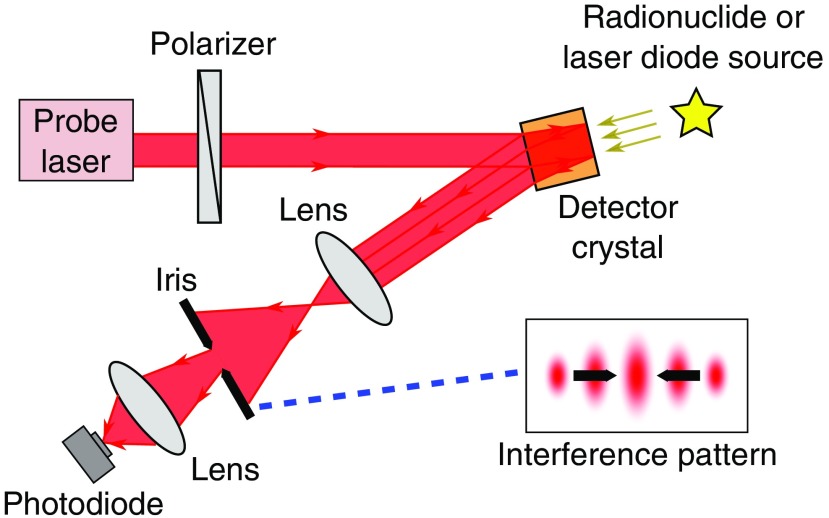
In this study, we used the same two-beam interference setup as in our previous work14 to achieve the optics pump-probe measurement. The schematic for the optical setup is shown in Fig. 1. A tunable C-band probe laser (Agilent N7714A Tunable Laser Source, with central wavelength around 1550 nm) is first linearly polarized and then illuminates the detector crystal (CdTe or BSO). The laser beams reflected from the front and rear surfaces of the crystal interfere with each other and generate an interference pattern (shown in the inset). The interference pattern is expanded with a lens. An optical iris is placed after the lens to allow only a fixed portion of the interference pattern to pass through (shown by the black arrows in the inset). The light transmitted through the iris is further focused by another lens and detected with a photodiode detector. The detected light intensity is the signal being monitored during the experiment. The detector crystal is DC biased and the entire setup is put in a light tight box during the experiment.
Fig. 1.
Schematic of optical setup. The “signal” is represented by a spatial shift in the interference pattern caused by the creation of charge carriers in the crystal.
The ionization-induced optical property modulation mechanism employed in this work is the linear electro-optic effect (i.e., Pockels effect) in the detector crystal. Both CdTe and BSO are Pockels cells.18,19 The refractive index of a Pockels cell can be expressed as17
| (1) |
where is the material’s index of refraction with an electric field applied on the crystal, is the applied electric field amplitude, is the index with no electric field applied, and is the Pockels coefficient or linear electro-optic coefficient. The refractive index of a Pockels cell is linearly dependent on the applied electric field strength.
The optical phase difference between the two interfering beams in the experimental setup can be expressed as
| (2) |
where is the optical phase difference, is the refractive index of the detector crystal (CdTe or BSO), is the vacuum wavelength of the probe laser, and is the geometric path length difference between the two interfering beams, which is a fixed value and approximately equals twice the detector crystal thickness here.
When ionizing radiation photons interact with the detector crystal, charge carriers are created through impact ionization. These carriers drift toward the two electrodes at the crystal surface due to applied bias voltage. Consequently, local charge separation and current flow occur, and thus a change in the local electric field strength is generated. According to Eq. (1), the refractive index of the detector crystal is changed as a result. This also modifies the optical phase difference between the two interfering beams according to Eq. (2). Since the interference pattern is determined by the optical phase difference, interference fringes (see Fig. 1) shift in space accordingly and then shift back as the space charge clears. The detected intensity of the light passing through the iris is modulated in response. Therefore monitoring the detected light intensity modulations allows us to detect the interaction of ionizing radiation photons.
2.3. Measuring Current–Voltage Curve
The resistivity of the detector crystal is an important influencing factor for the experiment. Therefore we first measured the current–voltage characteristic (or curve) for the two detector crystals. A Keithley Femtoamp Sourcemeter was used to achieve the detection of weak current flow in the detector crystals.
2.4. Testing Setup Feasibility
To test the feasibility of using the detector crystals in the two-beam interference setup, we started the experiment with no radiation source present. We first kept the bias voltage fixed (zero bias voltage) and studied the dependence of the signal magnitude (transmitted laser intensity through the optical iris as shown in Fig. 1) on the probe laser wavelength, then measured the signal magnitude dependence on the bias voltage at a fixed operating wavelength (1550.000 nm).
2.5. Using Laser Diode as the Source of Ionization
We first used a 405-nm laser diode (CEL NV4V31SF) as a controllable source of ionization to observe the optical modulation signal. We recorded the optical signal level change when the detector crystal was illuminated by laser diode light pulses. The oscilloscope (Agilent DSO90404A) that we used to record the optical signal was triggered by the drive voltage of the laser diode. In addition, we measured the dependence of the modulation signal amplitude on detector crystal bias voltage.
2.6. Using Ge-68 as the Source of Ionization
We then studied how the detector crystals would react to annihilation photons. A Ge-68 source, which emits 511-keV photons, was used for the experiment. The source was repetitively placed close to the detector crystal and then removed. We recorded the optical signal level change between the situations when the source was present and when the source was removed. For each measurement, we recorded the stable optical signal level observed at 1 min after placing or removing the source. This is because during the transition between placing the source close to the detector crystal and taking the source away, the signal did not change instantaneously. Instead, the response to the presence or removal of the source took several seconds to several minutes depending on the source activity. After this settling time, the signal level would remain stable around a fixed value. Therefore, we choose to wait 1 min for the signal to stabilize and then read each data point as the stable signal level, which was done similarly in our previous work.14 Each data point (the stable signal level) was recorded as a histogram of the optical signal magnitude for 1 min. The value corresponding to the histogram peak was taken as the magnitude of the stable signal level, and the peak width (full width at half maximum) was used as the error bar. All the data points were taken successively in time. Additionally, we also studied the dependence of the modulation signal amplitude on detector crystal bias voltage.
3. Results
3.1. Current–Voltage Curve
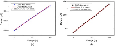
The curves for CdTe and BSO crystals are shown in Fig. 2. From the measurements, we estimated the resistivity for the two crystals as for CdTe and for BSO. We can see that the resistivity of the BSO crystal is much higher than CdTe. With the same dimensions, BSO crystal therefore has a much larger resistance.
Fig. 2.
curves for (a) CdTe and (b) BSO.
3.2. Setup Feasibility Tests
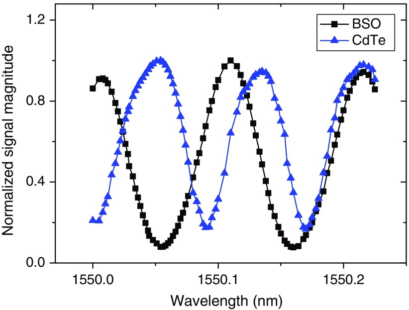
The dependence of the signal magnitude on the probe laser wavelength at zero bias voltage is shown in Fig. 3. The signal magnitude is normalized for clear comparison. This figure looks different from the probe laser wavelength dependence figure in our previous work14 since the data were taken at different crystal bias voltage conditions and with a different crystal orientation and laser alignment. According to Eq. (2), the optical phase difference between the two interfering beams is modulated as the probe laser wavelength is tuned. This modulation results in a spatial shift of the transmitted interference fringes as discussed in Sec. 2.2. Therefore, bright and dark fringes pass through the optical iris successively and are detected. This explains the oscillating pattern in Fig. 3. From the graph, we can see that both crystals can work in the interference setup since tuning the operating wavelength generates an oscillating pattern of the transmitted light intensity for both crystals. The similar oscillation period is due to the identical dimensions and similar refractive indices of the crystals. The slightly longer period of BSO crystal is related to its lower refractive index. We can see this from Eq. (2) since a crystal with a lower refractive index will require a longer wavelength tuning range to reach the same phase shift. Different fringe extinction ratios (intensity ratio between bright and dark fringe or the ratio between the highest and lowest signal magnitude as shown in Fig. 3) are related to crystal surface finish quality.
Fig. 3.
Dependence of signal magnitude on probe laser wavelength.
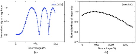
The dependence of the signal magnitude on the crystal bias voltage at 1550-nm probe laser wavelength is shown in Fig. 4. The signal magnitude is normalized for clear comparison. To facilitate an informative comparison, this figure presents the same set of data as used for the crystal bias dependence figure in our previous work.14 According to Eq. (1), changing the bias voltage (thus the electric field) changes the refractive index of the detector crystal. According to Eq. (2), this further modulates the optical phase difference between the two interfering beams. Therefore oscillations in the signal magnitude were observed corresponding to crystal bias voltage tuning as shown in Fig. 4 similar to Fig. 3. This result proves the Pockels effect in both CdTe and BSO crystals. It also shows the feasibility of using this setup (see Fig. 1) for detecting a modulation in the refractive index of the detector material. The longer oscillation period of BSO crystal is related to its higher resistivity, which is discussed in detail in Sec. 4.
Fig. 4.
Dependence of signal magnitude on crystal bias voltage for (a) CdTe and (b) BSO.
3.3. Results with Laser Diode as the Source of Ionization
The optical modulation signal induced by a laser diode as the source of ionization is shown in Fig. 5 for CdTe and BSO. The data for CdTe were taken under a crystal bias voltage at 1000 V, and the data for BSO were taken at 3500 V. Here, we show the modulation signal for the two crystals at different bias voltages in order to clearly show the shape of the modulation signal. The amplitude comparison of the modulation signal induced in the two crystals at different crystal bias voltages will be shown next. The blue dashed line in Fig. 5 shows the drive voltage of the laser diode, and the red solid line shows the optical signal level being modulated. Since the modulation signal is a small AC signal on top of a large DC signal (which is the average optical signal level) and since the modulation amplitude is proportional to the average optical signal level (which is also proportional to the probe laser intensity), here, we have normalized the modulated optical signal level to the average signal level in order to exclude the influence of different probe laser intensity and to show a clearer comparison between the two crystals. We have also normalized the laser diode drive voltage since the exact drive voltage value is not important here. From Fig. 5, we can see that the optical signal level is modulated by each light pulse of the laser diode due to refractive index modulation in the detector crystal. The relatively long decay edge of BSO signal is related to the low carrier mobility of the crystal, which is discussed in detail in Sec. 4.
Fig. 5.
Optical modulation signal induced by laser diode as the source of ionization for (a) CdTe and (b) BSO.
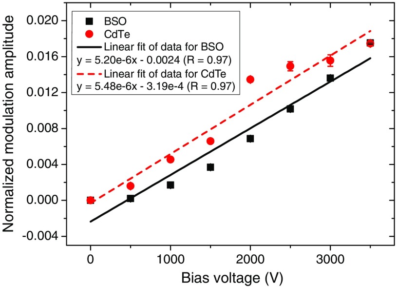
The dependence of the modulation signal (induced by laser diode) amplitude on crystal bias voltage is shown in Fig. 6 for both CdTe and BSO crystals. As explained above, the modulation signal is a small AC signal on top of a large DC signal (the average optical signal level) and the modulation amplitude is proportional to the average optical signal level (which is also proportional to the probe laser intensity). Therefore in Fig. 6, we have normalized the modulation amplitude (amplitude of the small AC signal) to the average optical signal level (magnitude of the large DC signal) in order to exclude the influence of different probe laser intensity and to show a clearer comparison between the two crystals. We can see that the modulation signal amplitude increases linearly with the crystal bias voltage. Increasing the crystal bias voltage leads to stronger optical modulation strength.
Fig. 6.
Dependence of laser diode induced modulation signal amplitude on crystal bias voltage.
3.4. Results with Ge-68 as the Source of Ionization
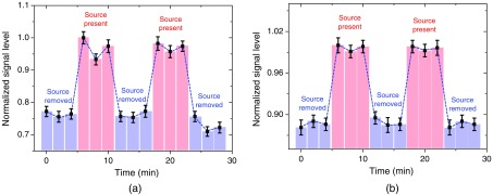
The optical modulation signal induced by Ge-68 as the source of ionization is shown in Fig. 7 for CdTe and BSO. For similar reasons as discussed in Sec. 3.3, here we show the data for CdTe taken under a crystal bias voltage at 1000 V and the data shown for BSO were taken at 3500 V. We have also normalized the modulated optical signal magnitude to the average optical signal level for clear comparison. The (higher) red shaded regions represent the optical signal magnitude when the Ge-68 source is placed close to the detector crystal and the blue (lower) shaded regions represent the signal level when the source is removed. We can see that both CdTe and BSO crystals can respond to 511-keV photon irradiation and the optical signal level is modulated by the presence of Ge-68 due to refractive index modulation in the detector crystal.
Fig. 7.
Optical modulation signal induced by Ge-68 as the source of ionization for (a) CdTe and (b) BSO.
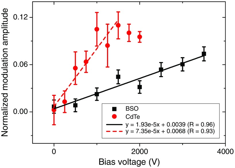
The dependence of the modulation signal (induced by Ge-68) amplitude on crystal bias voltage is shown in Fig. 8 for both CdTe and BSO crystals. For similar reasons as discussed in Sec. 3.3, the modulation signal amplitude is normalized to the average optical signal level in the graph. We can see that increasing the crystal bias voltage also leads to stronger optical modulation strength for Ge-68 induced modulation signal. The modulation signal induced in CdTe tends to saturate at bias voltage larger than 1500 V and thus the last two data points were not included in the linear fitting. We will discuss this point in Sec. 4.
Fig. 8.
Dependence of Ge-68 induced modulation signal amplitude on crystal bias voltage.
4. Discussion
We can see from Fig. 3 that the wavelength dependence curve of BSO crystal is smoother than that of CdTe crystal and has a higher fringe extinction ratio (defined in Sec. 3.2). This is because the BSO crystal has a better surface finish quality. It was also observed from the experiment that the interference fringes generated with the BSO crystal were clearer (with higher fringe extinction ratio) and easier to experiment with. These properties could be advantageous if we can integrate BSO crystals into a real detector module.
From Fig. 4, we can see that the low resistivity CdTe crystal experienced three oscillation periods from 0 V to 1500 V. The high resistivity BSO only went over less than a quarter oscillation period from 0 V to 3500 V. It was also found during the experiment that when limiting the output current of the crystal bias voltage power supply, even when we continued to increase the output voltage, the optical signal level was not modulated any more. We can conclude that the induced current flow (by tuning the crystal bias voltage here) in the detector crystal determines the strength of the optical modulation, not the absolute bias voltage.
We can see from Fig. 5 that the modulation signal induced by a laser diode in the BSO crystal has a longer decay edge. This signal decay is due to the charge carrier clearing process in the detector crystal and thus the decay speed is related to the carrier drift velocity, which further depends on the carrier mobility in the detector crystal. If we focus on electrons here, the electron mobility in CdTe is approximately 18 and the electron mobility in BSO is around .20 Taking into account the bias voltage difference (1000 V for CdTe and 3500 V for BSO), we can estimate that the electron drift velocity in CdTe is about 50 times larger than that in BSO. By analyzing the decay edge of the modulation signals in Fig. 5,21 we can calculate that the decay time constant is around for the CdTe crystal and approximately 8.5 ms for BSO. Therefore the decay time constant in BSO is about 50 times longer than that in CdTe, which matches the ratio between the electron drift velocities in the two crystals. We have thus concluded that the relatively long decay edge of BSO signal is related to the low carrier mobility of the crystal. The ideal detector material needs to have high carrier mobility, thus a short detector dead time, in order to achieve the detection of individual 511-keV photon interactions and accommodate for high count rate.
Figure 6 shows that CdTe and BSO crystals can achieve similar sensitivity under laser diode illumination at the same crystal bias voltage condition. However, the long decay edge of BSO crystal’s modulation signal as shown in Fig. 5(b) might lead to a relatively long dead time when using BSO as the detector material.
From Fig. 8, we can see that the BSO crystal is not as sensitive to 511-keV photons as the CdTe crystal under the same crystal bias voltage. The different detection sensitivity of the two crystals is a combined result caused by the differences between their properties including the electro-optic coefficient, 511-keV photon attenuation coefficient, and bandgap energy as shown in Table 1. The CdTe crystal has a larger electro-optic coefficient, which can lead to stronger optical modulation signal. However, the BSO crystal has a higher 511-keV photon attenuation coefficient, which enables it to absorb more energy from the ionizing radiation photons and generate more charge carriers. A larger number of ionization-induced charges will increase the optical modulation strength. The bandgap energy of the crystal, which is indirectly related to the carrier creation energy, also affects the number of charge carriers created by 511-keV photon interactions and thus influences the optical modulation strength. The CdTe crystal has a lower bandgap energy and it is expected that more carriers are created in this crystal. These factors in combination result in the difference between the material’s detection sensitivity.
During the experiment, we also observed that the signal level tended to drift more severely with the low resistivity CdTe crystal than the high resistivity BSO crystal under high crystal bias. This is believed to be related to the large dark current induced in the CdTe crystal under high crystal bias voltage, which further explains the larger error bars for CdTe in Fig. 8. In addition, the modulation signal with CdTe tends to saturate at bias voltage larger than 1500 V while the signal with BSO still goes up after 3500 V. This is also related to the lower resistivity (and thus larger dark current) in the CdTe crystal. Since the current flow induced by ionizing radiation photon interactions in the detector crystal determines the strength of the optical modulation, a large dark current will interfere with this radiation-induced current and make further increase in the optical modulation strength undetectable. With a high resistivity, the BSO crystal does not suffer from signal saturation up to 3500 V. Based on the linear relation between the optical modulation strength and crystal bias voltage, we believe that further increasing the bias voltage for BSO could potentially further increase the modulation strength and thus improve its detection sensitivity. Due to experimental equipment limit, this assumption was not tested out here but will be studied in our future work. We will also further study if the electron multiplication effect with even higher crystal bias voltage can be used to significantly boost the optical modulation strength in order to improve detection sensitivity. In addition to the high resistivity, the low cost and better crystal surface finish quality of the BSO crystal are also desirable for building a real PET detector module with the detection approach discussed in this work.
5. Conclusion and Future Work
In this work, we have compared the performance of CdTe and BSO as two detector crystals for the optical property modulation-based radiation detection method for PET and discussed desired properties of an ideal detector material. Both crystals can work for this approach and we have observed the modulation signal induced by either a laser diode or a Ge-68 source as the source of ionization with both crystals. The BSO crystal has a lower cost, better crystal surface finish quality, and higher resistivity, thus lower dark current noise, than the CdTe crystal. However, the CdTe crystal has higher carrier mobility, thus shorter detector dead time, than the BSO crystal. The CdTe and BSO crystals can achieve the same detection sensitivity under laser diode illumination at the same crystal bias voltage condition. However, the BSO crystal is not as sensitive to 511-keV photons as the CdTe crystal under the same crystal bias voltage before saturation. Further increasing the bias voltage for BSO could potentially further enhances the modulation strength and thus its detection sensitivity.
For the future work, we will focus on advancing the sensitivity of our experimental setup to be able to see the effects of single 511-keV photons with temporal resolution in the range of picoseconds. In addition to identifying more suitable detector materials based on the results presented in this work, we will also explore other aspects to achieve this goal. First of all, as discussed in Sec. 4, we will further study if the electron multiplication effect with even higher crystal bias voltage can be exploited to significantly boost the optical modulation signal strength. Additionally, we plan to make use of the optical amplification effect with high quality factor (high-) optical cavities to dramatically improve the detection sensitivity of the experimental setup.22 In order to prove that the optical modulation effects in detector materials occur within picosecond or even femtosecond scale, we will make use of ultrafast laser and X-ray sources to probe the intrinsic material properties and possible ultrafast optical modulation processes.
Acknowledgments
This work was funded in part by the National Institutes of Health-National Institute of Biomedical Imaging and Bioengineering (NIH-NIBIB) Grant No. R21EB015155.
Biographies
Li Tao is a graduate student at the Molecular Imaging Instrumentation Laboratory, Stanford University. She received her BS degree in optics from Fudan University, China, in 2012. Her current research interests focus on probing radiation-induced optical property modulations in photorefractive materials for faster timing in time-of-flight-positron emission tomography systems.
Henry M. Daghighian has over 29 years of experience in industry with specialization in device physics, microwave electronics, and photonics. He is a senior member of IEEE and holds 22 US patents.
Craig S. Levin is currently a professor of the Department of Radiology and has courtesy appointments with the Departments of Electrical Engineering, Physics, and Bioengineering at Stanford University. He is a founding member of the Molecular Imaging Program at Stanford and faculty member of the Bio-X Program, Cancer Institute, Neuroscience Institute, and Cardiovascular Institute, Stanford. He is also the director of the Molecular Imaging Instrumentation Laboratory (miil.stanford.edu) at Stanford University.
Disclosures
No conflicts of interest, financial or otherwise, are declared by the authors.
References
- 1.Gambhir S. S., “Molecular imaging of cancer with positron emission tomography,” Nat. Rev. Cancer 2(9), 683–693 (2002). 10.1038/nrc882 [DOI] [PubMed] [Google Scholar]
- 2.Bailey D. L., et al. , Positron Emission Tomography, Springer, London: (2005). [Google Scholar]
- 3.Juweid M. E., Cheson B. D., “Positron-emission tomography and assessment of cancer therapy,” N. Engl. J. Med. 354(5), 496–507 (2006). 10.1056/NEJMra050276 [DOI] [PubMed] [Google Scholar]
- 4.Karp J. S., et al. , “Benefit of time-of-flight in PET: experimental and clinical results,” J. Nucl. Med. 49(3), 462–470 (2008). 10.2967/jnumed.107.044834 [DOI] [PMC free article] [PubMed] [Google Scholar]
- 5.Surti S., et al. , “Investigation of time-of-flight benefit for fully 3-D PET,” IEEE Trans. Med. Imaging 25(5), 529–538 (2006). 10.1109/TMI.2006.871419 [DOI] [PubMed] [Google Scholar]
- 6.Fazel R., et al. , “Exposure to low-dose ionizing radiation from medical imaging procedures,” N. Engl. J. Med. 361(9), 849–857 (2009). 10.1056/NEJMoa0901249 [DOI] [PMC free article] [PubMed] [Google Scholar]
- 7.Pratx G., et al. , “Fast, accurate and shift-varying line projections for iterative reconstruction using the GPU,” IEEE Trans. Med. Imaging 28(3), 435–445 (2009). 10.1109/TMI.2008.2006518 [DOI] [PMC free article] [PubMed] [Google Scholar]
- 8.Levin C. S., Hoffman E. J., “Calculation of positron range and its effect on the fundamental limit of positron emission tomography system spatial resolution,” Phys. Med. Biol. 44(3), 781–799 (1999). 10.1088/0031-9155/44/3/019 [DOI] [PubMed] [Google Scholar]
- 9.Lecoq P., et al. , Inorganic Scintillators for Detector Systems: Physical Principles and Crystal Engineering, Springer Science & Business Media, Berlin Heidelberg: (2006). [Google Scholar]
- 10.Lecoq P., Korzhik M., Vasiliev A., “Can transient phenomena help improving time resolution in scintillators?” IEEE Trans. Nucl. Sci. 61(1), 229–234 (2014). 10.1109/TNS.2013.2282232 [DOI] [Google Scholar]
- 11.Cates J. W., Vinke R., Levin C. S., “Analytical calculation of the lower bound on timing resolution for PET scintillation detectors comprising high-aspect-ratio crystal elements,” Phys. Med. Biol. 60(13), 5141–5161 (2015). 10.1088/0031-9155/60/13/5141 [DOI] [PMC free article] [PubMed] [Google Scholar]
- 12.Keiser G., Optical Fiber Communications, Wiley Online Library, Hoboken, New Jersey: (2003). [Google Scholar]
- 13.Almeida V. R., et al. , “All-optical control of light on a silicon chip,” Nature 431(7012), 1081–1084 (2004). 10.1038/nature02921 [DOI] [PubMed] [Google Scholar]
- 14.Tao L., Daghighian H. M., Levin C. S., “A promising new mechanism of ionizing radiation detection for positron emission tomography: modulation of optical properties,” Phys. Med. Biol. 61(21), 7600–7622 (2016). 10.1088/0031-9155/61/21/7600 [DOI] [PMC free article] [PubMed] [Google Scholar]
- 15.Esseling M., et al. , “Opto-electric particle manipulation on a bismuth silicon oxide crystal,” Appl. Phys. Lett. 100(16), 161903 (2012). 10.1063/1.4704361 [DOI] [Google Scholar]
- 16.Tan W., et al. , “High time-resolved three-dimensional imaging using ultrafast optical Kerr gate of bismuth glass,” IEEE Photonics Technol. Lett. 23(8), 471–473 (2011). 10.1109/LPT.2011.2109704 [DOI] [Google Scholar]
- 17.Saleh B. E., Teich M. C., Saleh B. E., Fundamentals of Photonics, Vol. 22, Wiley, New York: (1991). [Google Scholar]
- 18.Bell R., “Review of optical applications of CdTe,” Rev. Phys. Appl. 12(2), 391–399 (1977). 10.1051/rphysap:01977001202039100 [DOI] [Google Scholar]
- 19.Mullen R., Hellwarth R., “Optical measurement of the photorefractive parameters of ,” J. Appl. Phys. 58(1), 40–44 (1985). 10.1063/1.335694 [DOI] [Google Scholar]
- 20.Biaggio I., Hellwarth R. W., Partanen J. P., “Band mobility of photoexcited electrons in ,” Phys. Rev. Lett. 78(5), 891–894 (1997). 10.1103/PhysRevLett.78.891 [DOI] [Google Scholar]
- 21.Pierret R. F., et al. , Semiconductor Device Fundamentals, Addison-Wesley Reading, Massachusetts: (1996). [Google Scholar]
- 22.Armani A. M., et al. , “Label-free, single-molecule detection with optical microcavities,” Science 317(5839), 783–787 (2007). 10.1126/science.1145002 [DOI] [PubMed] [Google Scholar]


