Abstract
The influences of annealing temperature in N2 atmosphere on interfacial chemical properties and band alignment of AlN/Si structure deposited by atomic layer deposition have been investigated based on x-ray photoelectron spectroscopy and spectroscopic ellipsometry. It is found that more oxygen incorporated into AlN film with the increasing annealing temperature, resulting from a little residual H2O in N2 atmosphere reacting with AlN film during the annealing treatment. Accordingly, the Si–N bonding at the interface gradually transforms to Si–O bonding with the increasing temperature due to the diffusion of oxygen from AlN film to the Si substrate. Specially, the Si–O–Al bonding state can be detected in the 900 °C-annealed sample. Furthermore, it is determined that the band gap and valence band offset increase with increasing annealing temperature.
Background
AlN is considered to be a promising semiconductor material because of its wide direct band gap, high piezoelectric response and small mismatches of lattice constant, and thermal expansion coefficient with Si substrate. It is these advantages of AlN material that has made it an attractive candidate material for numerous applications in various optoelectronic and microelectronic devices on Si substrate [1–3]. Bulk AlN has a high dielectric constant of 9, and the interface between AlN and Si is established to be thermally stable. Preparing AlN/Si metal-insulator-semiconductor (MIS) structures with acceptable qualities will thus open the path to co-integration of light emitting nitrides with silicon microelectronics [4, 5]. Silicon field-effect transistors using AlN as gate dielectric have been demonstrated by several studies with good performance [6, 7]. So far, many deposition methods have been pursued to obtain AlN films, such as molecular beam expitaxy (MBE) [8], metal-organic chemical vapor deposition (MOCVD) [9], and sputtering [10]. Considering a promising deposition method for AlN film, atomic layer deposition (ALD) has its unique advantage in uniformity, conformality, and thermal budget. Besides these properties mentioned above, ALD is also an excellent deposition method to control the thickness of the AlN film at a single atom layer scale.
In addition, AlON is also a promising material as gate insulator with a dielectric constant as high as 13. Furthermore, it is reported that the AlON layer can provide a prevention of silicon diffusion to the gate insulator [11, 12]. Inserting AlON layer between HfO2 gate oxide and Si substrate can suppress the interlayer between AlON and Si resulting in a high quality channel layer [13, 14]. As is known, film properties of AlON can be tailored between those of pure aluminum nitride (AlN) and aluminum oxide (Al2O3), depending on different applications [15].
Experimentally, the as-deposited AlN thin films usually not only possess a little of oxygen, but also easily form AlON compounds with the subsequent high temperature thermal treatments [16–18]. However, the annealing temperature dependence on the interfacial chemical properties and band alignment of the ALD-AlN/Si structure has not been thoroughly investigated, which plays an important part in the electronic properties of the corresponding device. As a result, thermal ALD system is used to grow thin AlN film on Si substrate in this work. The effect of annealing temperature under N2 ambient on the interfacial chemical bonding states of the obtained AlN/Si structure have been investigated by x-ray photoelectron spectroscopy (XPS) in detail. Furthermore, the electronic energy band alignment of the heterojunction structure is also determined as a function of N2 annealing temperature.
Methods
Thin AlN film with 70 cycles (~6.5 nm) was deposited on p-type silicon wafer with crystal orientation of (100) and sheet resistivity of 2~4 Ω cm using atomic layer deposition (ALD) at 370 °C. The precursors trimethylaluminum (TMA) and NH3 have been utilized as Al and N sources, respectively. Prior to the growth of AlN films, the Si substrates were cleaned using the Radio Corporation of America (RCA) cleaning process and then dipped into a 2% hydrofluoric acid (HF) aqueous solution for 2 min to remove the native oxides. To investigate the effect of the high temperature annealing on the interfacial chemical properties of the AlN/Si structure, ex situ post-deposition rapid thermal annealing (RTA) was conducted under N2 ambient condition with a temperature range of 600–900 °C for 60 s. An ex-situ SPECS XPS system with a monochromatic Al Kα source (hv = 1486.6 eV) for the excitation of photoelectrons was utilized for data acquisition. The source power was 150 W (10 kV, 15 mA) and the analysis region was a round spot with a radius of 500 μm, an incident angle of 58o, and a takeoff angle of 90o. Broad band scans with a step of 0.5 eV and pass energy of 25 eV are performed twice in order to acquire the binding energy of specific elements. Charge neutralization was performed with an electron flood gun. Narrow scans with a step of 0.05 eV and pass energy of 25 eV are performed for 20 times for binding energy of specific elements. Furthermore, the valence band scans with a step of 0.05 eV and pass energy of 25 eV are performed for 30 times to obtain the valence band spectra. Charge correction is performed using the position of C 1 s spectra at 284.6 eV. Moreover, the XPS spectrometer energy scale was calibrated using Ag 3d 5/2, Cu 2p 3/2, and Au 4f 7/2 photoelectron lines located at 368.06, 932.47, and 83.78 eV, respectively. Spectral deconvolution was performed by Shirley background subtraction using a Voigt function convoluting the Gaussian and Lorentzian functions. Spectroscopy ellipsometry measurements were also performed using a commercial instrument (Sopra GES5E, SOPRA, Courbevoie, France) to obtain the band gap and thickness of AlN film where the incident angle was fixed at 75°, and the wavelength region from 190 to 900 nm was scanned with 5-nm steps.
Results and Discussion
In order to investigate the evolution of the interfacial chemical states of AlN/Si structures related with the annealing temperature, the profiles of Al, N, and Si chemical states were examined using XPS. Figure 1 shows the Al 2p XPS spectra with the thermal annealing treatment. It is evident that the Al 2p for all of the samples can be fitted by two subpeaks located at 73.5 ± 0.1 and 74.6 ± 0.1 eV, corresponding to Al–N and Al–O bonds, respectively. The binding energy positions are in good agreement with the reported results [19]. For the as-deposited sample, the Al–O bonds can be attributed to surface oxidation of AlN layer due to the exposure to air during transporting the sample to the XPS system. Similar results were reported for AlN films deposited by PEALD using NH3 plasma on Si substrate [20]. Moreover, the intensity of the Al–N subpeak attenuates and the Al–O subpeak increases relatively with increasing the annealing temperature, suggesting that more oxygen incorporated into AlN film, leading to formation of more Al–O at higher annealing temperature in the N2 ambient. The oxygen concentration is originated from the trace amounts of residual H2O contained in the N2 atmosphere. The increase in the Al–O/Al–N intensity ratio after RTA can be attributed to the breakage of Al–N bonds which are metastable with respect to O. In order to understand the oxidation of AlN film, the atomic ratio of N/Al was calculated to be 0.76, 0.32, 0.31, 0.23, and 0.14 for the as-deposited, 600, 700, 800, and 900 °C annealed sample, respectively. It suggests that the breakage of Al–N bonds is more intense with the increasing annealing temperature. This is in good agreement with reported results, where a strong N loss from the previously N-rich AlN film was observed after vacuum and O2 RTAs [11]. Figure 2 shows the N 1 s spectra of the as-deposited and subsequently annealed AlN samples at 600, 700, 800, and 900 °C, respectively. For the as-deposited sample, the fitted three peaks located at binding energies of 396.4, 398.0, and 394.6 eV are attributed to N–Al, N–Al–O, and N–N bonding states, respectively. It shall be noticed that the dominant N–Al bonding and N–Al–O bonding can be detected in all the samples, but the N–N bonding only exists in the as-deposited one. With the annealing temperature increasing, the N–Al–O subpeak is observed to decrease in intensity as the annealing temperature increases. It suggests that the three-component system of N–Al–O decomposed into Al–N and Al–O under higher temperature. This is in good accordance with the result of the situation of AlN/AlGaN/GaN system annealing in N2 atmosphere [21]. In fact, both N–Al and N–Al–O subpeaks are observed to decrease in intensity as the annealing temperature increases. Nevertheless, the decomposition of N–Al bonds is more intense than the one of N–Al–O when the annealing temperature reaches to 900 °C. Therefore, it looks like the intensity of N–Al–O bonds enhanced relative to the N–Al bonds.
Fig. 1.
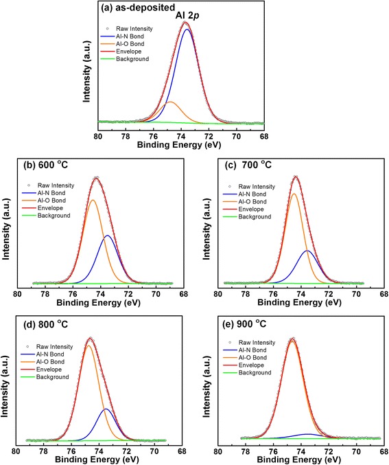
Al 2p photoelectron spectra of AlN/Si structures: a as-deposited, b annealed at 600 °C, c annealed at 700 °C, d annealed at 800 °C, and e annealed at 900 °C for 60 s in N2 ambient
Fig. 2.
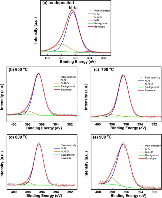
N 1 s photoelectron spectra of AlN/Si structures: a as-deposited, b annealed at 600 °C, c annealed at 700 °C, d annealed at 800 °C, and e annealed at 900 °C for 60 s in N2 ambient
The Si 2p core-level spectra for the AlN/Si structures taken at normal emission setup for as-deposited and annealing samples are shown in Fig. 3. It can be noted for all the samples that the subpeak located at lower binding energy side is composed of two spin-orbit split peaks Si 2p 1/2 and Si 2p 3/2 owing to Si substrate. The two peaks are located at 99.8 and 99.2 eV, respectively, with a spin orbit split (S.O.S) of 0.6 eV and an intensity ratio of 1:2. For the as-deposited sample and 600 °C annealing sample, the Si 2p subpeak located at 101.8 eV is correlated to Si–N bond states, which is in good agreement with the reported results [22]. The Si–N bonding at the interface of AlN/Si heterostructure is beneficial to the surface passivation of the Si substrate and proved to be chemically stable. When the annealing temperature increases to 700 and 800 °C, it can be seen that the Si–N bonding disappears completely. However, a new Si 2p subpeak with a binding energy of 102.7 ± 0.1 eV can be detected, which can be assigned to the formed interfacial SiOx (x < 2) layer during thermal annealing [23]. With the increase of annealing temperature from 700 to 800 °C, the intensity of Si–O subpeak increases and shifts toward high binding energy sides, resulting from the complete oxidation of the suboxides involved in the interfacial layer. The formation of Si–O bonds during annealing treatment is caused by the diffusion of the oxygen contained in the AlN film and the trace amount of residual H2O contained in the N2 atmosphere. Comparing the 600 °C annealing sample with the as-deposited sample, it can be seen that the Al–O/Al–N intensity ratio increases dramatically. But for Si 2p spectrum, there are still Si–N bondings but not any Si–O bonds at the interface, suggesting that at 600 °C the AlN film protected the Si substrate from oxidation near the interface. In addition, after the sample annealed at 900 °C, another new peak at 103.33 eV corresponding to the Si–O–Al bonds can be found, confirming the formation of silicate layer. It suggests that the interfacial property of AlN/Si structure has degraded significantly after 900 °C annealing [24].
Fig. 3.
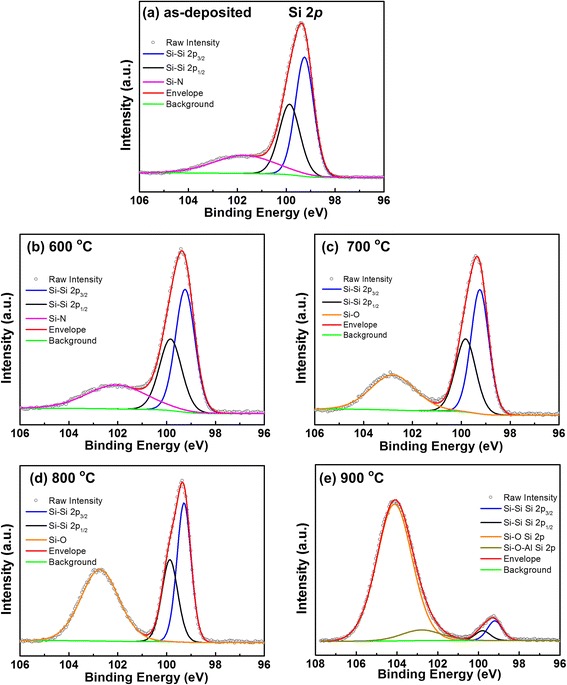
Si 2p photoelectron spectra of AlN/Si structures. a As-deposited, b annealed at 600 °C, c annealed at 700 °C, d annealed at 800 °C, and e annealed at 900 °C for 60 s in N2 ambient
In addition to the interfacial analysis, the band offsets of the AlN/Si samples with thermal treatment are also investigated based on the fact that the band alignment is one of the most fundamental physical properties for the application of semiconductor device. To determine the band offsets of the AlN/Si under different annealing temperatures, the bandgap (E g) of the as-prepared films will be determined firstly. In the case of AlN, the value of E g can be extracted from the experimental absorption coefficient assuming a direct transition of electrons from the valence band to the conduction band. Generally, the E g can be estimated by using the so-called Tauc’s method [25]
| 1 |
where α is the absorption coefficient, hυ is the incident photon energy, and A is a constant. The absorption coefficient α is related to the extinction coefficient (k) of the sample via α = 4πk/λ where λ is the wavelength of the incident light. The bandgap energy can be found by drawing relatively a linear fit line with a maximum negative slope in the curve. The tangent intersects with the horizontal axis and the crossing point gives the band gap value. It can be observed from Fig. 4, the band energies of the as-deposited and annealed samples from 600 to 900 °C are 5.75, 5.79, 5.80, 5.9,1 and 5.95 eV, respectively. The bandgap value of Al2O3 (6.8 eV) is larger than the one of AlN (6.0 eV) [26, 27]. With the increase in annealing temperature, the band energies of AlN increase owning to the incorporation of O element into the AlN film and the formation of Al2O3. It must be pointed out that the band gap value of as-deposited sample is less than the bulk AlN band gap value. It can be attributed to a variety of crystal defects in the prepared AlN layer, which may induce intermediate energy levels that merge with the conduction band, and lower the bandgap [17].
Fig. 4.
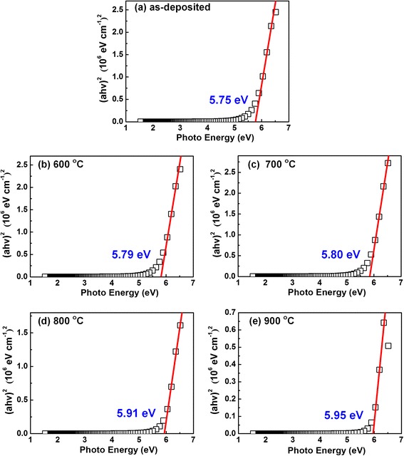
The bandgap energy of AlN films under various annealing temperature
Figure 5 presents the valence band spectra of AlN/Si structures determined by linear extrapolation method. Two slopes have been observed clearly, in which the slope in the lower binding energy regime is corresponding to the Si valence band onset and the one in the higher energy regime is corresponding to the AlN film valence band onset. The values of the valence band maximum (VBM) for the AlN film deposited on Si substrate under various annealing temperature are then determined to be 1.71, 3.44, 4.07, 4.34, and 5.07 eV, respectively. On the other hand, the valence band spectrum for the Si substrate is found to be located at 0.13 eV in Fig. 6. According to Kraut’s method [28], the valence band offset (ΔEv) and the conduction band offset (ΔEc) of AlN/Si interface can be described to the following equations:
| 2 |
| 3 |
Fig. 5.
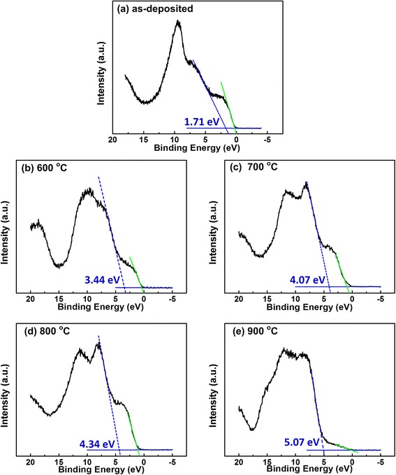
Valence band spectra of AlN/Si structures determined by extrapolation of the leading edge to the base line
Fig. 6.
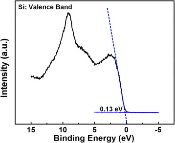
Valence band spectra of bulk Si determined by linear extrapolation method
where is the valence band maximum of AlN, is the valence band maximum of bulk Si, is the band gap of AlN, is the valence band offset, and band gap of the Si wafer. Based on the above equations, the valence band offset for the as-deposited AlN film is determined to be 1.58 eV. With the increase of the annealing temperature, the valence band offsets of 3.31, 3.94, 4.21, and 4.94 eV for the annealed samples on Si substrate has been also detected, respectively. It is observed that the valence band offset shifts toward higher energy with increasing the annealing temperature. As is well known, the predominant contribution to the AlN valence band is from the N 2p orbital [29], and the valence band maximum of Al2O3 is mainly determined by O 2p [30]. Therefore, the shift toward higher energy in the valence band maximum of AlN film with the annealing temperature is mainly on account of the generation of Al2O3. With the knowledge of the Si band gap value of 1.12 eV, ΔEc values for as-deposited and annealed from 600 to 900 °C samples are calculated to be 3.05, 1.36, 0.74, 0.58, and −0.11 eV, respectively. Figure 7 shows a summary of the schematic band diagram of the as-deposited and annealed AlN/Si structures at different temperatures. For the as-deposited and 600 °C annealed sample, both ∆Ec and ∆Ev values are over 1 eV, which satisfies the requirement to guarantee the sufficient barrier height in metal-insulator-semiconductor (MIS) application. When the temperature comes to 700 and 800 °C, and the ΔEc values are all found to be less than 1 eV, which could be utilized in optoelectronic device applications. Furthermore, for 900 °C annealed sample, the band structure changed to be type II band alignment. The feasibility to tune the band alignment of AlN/Si structure by selecting a proper annealing temperature shows advantage for AlN/Si structure used in different applications,where requires different band alignment types.
Fig. 7.
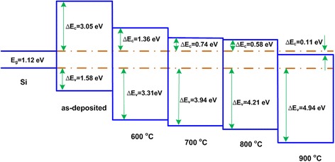
Schematic band diagram of the as-deposited and annealed AlN/Si structures
Conclusions
In summary, the influences of annealing temperature in N2 atmosphere on interfacial chemical properties and band alignment of AlN/Si structure prepared by thermal atomic layer deposition have been investigated. It has been found that more oxygen incorporated into AlN film with the increasing annealing temperature, resulting from a little residual H2O existed in N2 atmosphere reacting with AlN film during the annealing process. The Si–N bonding at the AlN/Si interface gradually transforms to Si–O bonding with the increasing temperature, due to the diffusion of oxygen from AlN film to the Si substrate. The band gap and valence band offset increase with increasing annealing temperature. These results indicate that the modification of the band structure of the AlN/Si heterojunction can be realized by properly selecting the annealing temperature.
Acknowledgements
This work is supported by the National Natural Science Foundation of China (No. 51102048, 61376008, 61376119, and U1632121), State Key Laboratory of Luminescence and Applications (Grant No. SKLA-2016-16), and the Innovation Program of Shanghai Municipal Education Commission (14ZZ004).
Authors’ Contributions
LS and HLL designed the study. LS, HYC, and TW carried out the deposition along with its characterization (XPS, SE) and interpretation of characterization. XMJ, WJL, SJD, DXZ, AD, and DWZ participated in the analysis and discussion of the results obtained from the experiments. HLL and DWZ supervised this study. The manuscript was prepared by LS, and HLL helped with draft editing. All authors approved and have equal contribution in drafting the final manuscript.
Competing Interests
The authors declare that they have no competing interests.
References
- 1.Zhao JL, Tan ST, Iwan S, Sun XW, Liu W, Chua SJ. Blue to deep UV light emission from a p-Si/AlN/Au heterostructure. Appl Phys Lett. 2009;94(9):093506. doi: 10.1063/1.3093489. [DOI] [Google Scholar]
- 2.Dubois M, Muralt P. Properties of aluminum nitride thin films for piezoelectric transducers and microwave filter applications. Appl Phys Lett. 1999;74(20):3032–3034. doi: 10.1063/1.124055. [DOI] [Google Scholar]
- 3.Witte H, Rohrbeck A, Günther KM, Saengkaew P, Bläsing J, Dadgar A, Krost A. Electrical investigations of AlGaN/AlN structures for LEDs on Si(111) Phys Status Solidi A. 2011;208(7):1597–1599. doi: 10.1002/pssa.201001146. [DOI] [Google Scholar]
- 4.Simeonov S, Bakalova S, Kafedjiiska E, Szekeres A, Grigorescu S, Sima F, Socol G, Mihailescu IN. Al/AlN/Si MIS structures with pulsed-laser-deposited AlN films as gate dielectrics: electrical properties. Rom J Inf Sci Technol (ROMJIST) 2007;10(3):251–259. [Google Scholar]
- 5.Adam T, Kolodzey J, Swann CP, Tsao MW, Rabolt JF. The electrical properties of MIS capacitors with AlN gate dielectrics. Appl Surf Sci. 2001;175:428–435. doi: 10.1016/S0169-4332(01)00091-5. [DOI] [Google Scholar]
- 6.Stevens KS, Kinniburgh M, Schwartzman AF, Ohtani A, Beresford R. Demonstration of a silicon field-effect transistor using AlN as the gate dielectric. Appl Phys Lett. 1995;66(66):3179–3181. doi: 10.1063/1.113715. [DOI] [Google Scholar]
- 7.Ingjar H (2014) Sputtering-deposited AlN film as the gate dielectric for n-MOSFETs Applications. J Info Tech Appl 8(1):20–23
- 8.Landré O, Fellmann V, Jaffrennou P, Bougerol C, Renevier H, Cros A, Daudin B. Molecular beam epitaxy growth and optical properties of AlN nanowires. Appl Phys Lett. 2010;96(6):061912. doi: 10.1063/1.3315943. [DOI] [Google Scholar]
- 9.Zang KY, Wang LS, Chua SJ, Thompson CV. Structural analysis of metalorganic chemical vapor deposited AlN nucleation layers on Si (1 1 1) J Cryst Growth. 2004;268(3–4):515–520. doi: 10.1016/j.jcrysgro.2004.04.083. [DOI] [Google Scholar]
- 10.Signore MA, Bellini E, Taurino A, Catalano M, Martucci MC, Cretì P, Quaranta F. Structural and morphological evolution of aluminum nitride thin films: influence of additional energy to the sputtering process. J Phys Chem Solids. 2013;74(10):1444–1451. doi: 10.1016/j.jpcs.2013.05.003. [DOI] [Google Scholar]
- 11.Soares GV, Bastos KP, Pezzi RP, Miotti L, Driemeier C, Baumvol IJR, Hinkle C, Lucovsky G. Nitrogen bonding, stability, and transport in AlON films on Si. Appl Phys Lett. 2004;84(24):4992–4994. doi: 10.1063/1.1763230. [DOI] [Google Scholar]
- 12.Henkel K, Karavaev K, Torche M, Schwiertz C, Burkov Y, Schmeißer D. Al-oxynitride interfacial layer investigations for PrXOY on SiC and Si. J Phys Conf Series. 2008;94:E349–E353. doi: 10.1088/1742-6596/94/1/012004. [DOI] [Google Scholar]
- 13.Choi W, Lee J, Yang J, Kim C, Hong J, Nahm TU, Byun B, Kim M. Analysis of chemical bond states and electrical properties of stacked AlON/HfO2 gate oxides formed by using a layer-by-layer technique. J Korean Phys Soc. 2006;48(6):1666–1669. [Google Scholar]
- 14.Choi W, Lee J, Yang J, Kim J, Hong J. Enhanced electrical and structural properties of stacked AlON∕HfO2 gate oxides on p-type Si substrates. J Vac Sci Technol B. 2007;25(4):400–405. doi: 10.1116/1.2756546. [DOI] [Google Scholar]
- 15.Bunjongpru W, Porntheeraphat S, Somwang N, Khomdet P, Hruanun C, Poyai A, Nukeaw J. Oxygen control on nanocrystal-AlON films by reactive gas-timing technique R.F. magnetron sputtering and annealing effect. Adv Mater Res. 2008;55-57:573–576. doi: 10.4028/www.scientific.net/AMR.55-57.573. [DOI] [Google Scholar]
- 16.Alevli M, Ozgit C, Donmez I, Biyikli N. Structural properties of AlN films deposited by plasma-enhanced atomic layer deposition at different growth temperatures. Phys Status Solidi A. 2012;209(2):266–271. doi: 10.1002/pssa.201127430. [DOI] [Google Scholar]
- 17.Motamedi P, Cadien K. Structural and optical characterization of low-temperature ALD crystalline AlN. J Cryst Growth. 2015;421:45–52. doi: 10.1016/j.jcrysgro.2015.04.009. [DOI] [Google Scholar]
- 18.Dalmau R, Collazo R, Mita S, Sitar Z. X-ray photoelectron spectroscopy characterization of aluminum nitride surface oxides: thermal and hydrothermal evolution. J Electron Mater. 2007;36(4):414–419. doi: 10.1007/s11664-006-0044-x. [DOI] [Google Scholar]
- 19.Rosenberger L, Baird R, Mccullen E, Auner G, Shreve G. XPS analysis of aluminum nitride films deposited by plasma source molecular beam epitaxy. Surf Interface Anal. 2008;40(9):1254–1261. doi: 10.1002/sia.2874. [DOI] [Google Scholar]
- 20.Van Bui H, Wiggers FB, Gupta A, Nguyen MD, Aarnink AAI, De Jong MP, Kovalgin AYJ. Initial growth, refractive index, and crystallinity of thermal and plasma-enhanced atomic layer deposition AlN films. Vac Sci Technol A. 2015;33(1):01A111–01A111-6. [Google Scholar]
- 21.Cao D, Cheng X, Xie Y, Zheng L, Wang Z, Yu X, Wang J, Shen D, Yu Y. Effects of rapid thermal annealing on the properties of AlN films deposited by PEALD on AlGaN/GaN heterostructures. RSC Adv. 2015;5(47):37881–37886. doi: 10.1039/C5RA04728E. [DOI] [Google Scholar]
- 22.Pélisson-Schecker A, Hug HJ, Patscheider J. Charge referencing issues in XPS of insulators as evidenced in the case of Al-Si-N thin films. Surf Interface Anal. 2012;44(1):29–36. doi: 10.1002/sia.3765. [DOI] [Google Scholar]
- 23.Wei HH, He G, Chen XS, Cui JB, Zhang M, Chen HS, Sun ZQ. Interfacial thermal stability and band alignment of Al2O3/HfO2/Al2O3/Si gate stacks grown by atomic layer deposition. J Alloys Compd. 2014;591:240–246. doi: 10.1016/j.jallcom.2013.12.152. [DOI] [Google Scholar]
- 24.Anderson PR, Swartz WE. X-ray photoelectron spectroscopy of some aluminosilicates. Inorg Chem. 1974;5(45):2293–2294. doi: 10.1021/ic50139a057. [DOI] [Google Scholar]
- 25.Tauc J (1966) Optical properties of semiconductors. The Optical Properties of Solids
- 26.Lu HL, Yang M, Xie ZY, Geng Y, Zhang Y, Wang PF, Sun QQ, Ding SJ, Zhang DW. Band alignment and interfacial structure of ZnO/Si heterojunction with Al2O3 and HfO2 as interlayers. Appl Phys Lett. 2014;104(16):161602. doi: 10.1063/1.4872175. [DOI] [Google Scholar]
- 27.Taniyasu Y, Kasu M, Makimoto T. An aluminium nitride light-emitting diode with a wavelength of 210 nanometres. Nature. 2006;441(7091):325–8. doi: 10.1038/nature04760. [DOI] [PubMed] [Google Scholar]
- 28.Kraut EA. Precise determination of the valence-band edge in x-ray photoemission spectra: application to measurement of semiconductor interface potentials. Phys Rev Lett. 1980;44(24):1620–1623. doi: 10.1103/PhysRevLett.44.1620. [DOI] [Google Scholar]
- 29.Choi J, Puthenkovilakam R, Chang JP. Band structure and alignment of the AlN/SiC heterostructure. Appl Phys Lett. 2005;86(19):192101. doi: 10.1063/1.1923187. [DOI] [Google Scholar]
- 30.Li XF, Fu YY, Liu XJ, Li AD, Li H, Wu D. Band alignment and interfacial properties of atomic layer deposited (TiO2)x(Al2O3)1−x gate dielectrics on Ge. Appl Phys A. 2011;105(3):763–767. doi: 10.1007/s00339-011-6511-0. [DOI] [Google Scholar]


