Abstract
Current lithography approaches underpinning the fabrication of microfluidic devices rely on UV exposure of photoresists to define microstructures in these materials. Conventionally, this objective is achieved with gas discharge mercury lamps, which are capable of producing high intensity UV radiation. However, these sources are costly, have a comparatively short lifetime, necessitate regular calibration, and require significant time to warm up prior to exposure taking place. To address these limitations we exploit advances in solid state sources in the UV range and describe a fast and robust wafer-scale laboratory exposure system relying entirely on UV-Light emitting diode (UV-LED) illumination. As an illustration of the potential of this system for fast and low-cost microfluidic device production, we demonstrate the microfabrication of a 3D spray-drying microfluidic device and a 3D double junction microdroplet maker device.
I. INTRODUCTION
Photolithography techniques that rely on transferring small scale structures from photomasks onto flat substrates using light represent one of the main fabrication routes in microelectronics and micro-devices,1,2 including microfluidics.3–5 Generally, radiation in the UV range is used to activate photoresists and the illumination is achieved commonly with gas-discharge lamps using mercury vapour. Such sources produce a wide spectrum of light and are coupled with filters to select the desired wavelength. Appropriate optics can then be used to collimate the light over the entire exposure area. However, such lamps require significant time to warm up, have a limited life time of typically 2000 hours for laboratory sources, and require regular calibration.
In an attempt to optimise the laboratory scale fabrication of microfluidic devices, we have explored solutions to simplify the photolithography step by exploiting progress in solid-state light emitting diode (LED) sources operating in the UV range. There are several requirements for an effective and accurate UV exposure source for lithography applications. First, the light used for photolithography should be uniform over a wafer scale to maintain compatibility with standard wafer substrates and to ensure that each area is exposed to the same dose of energy. Second, the emission spectrum should have a small bandwidth since the absorption in the photoresist is wavelength dependent. Finally, the illumination should be well collimated to ensure sharply defined features in the fabricated microstructures. All of these features can be achieved using light emitting diodes (LEDs) and UV transparent optical lenses. LEDs possess clear advantages over mercury lamps as they consume less electricity, they can be turned on and off within seconds, their life time is 20 000 hours, and they are cheap and extremely simple to use. However, until recently, the main limitation was their low power in the UV spectrum, which hindered their routine use for photolithography applications. This technical limitation has been overcome by assembling several LEDs into arrays.6–9 As such, new generation LED light sources have a high power source with integrated heat sink to keep the power at stable values, allowing their use for photolithography. We combine the exposure system with a micrometer positioning stage to allow multilayer lithography to be performed.
In view of the considerations above, we present here a highly versatile lab-scale UV-LED based photolithography set-up, with a mask aligner comprised of micrometric XYZ and rotation stages. The set-up addresses the main issues of conventional mercury lamp based mask aligners while retaining the resolution required for conventional microfluidic applications. In this paper, we describe the entire set-up in Section II and its characterisation in Section III. We show some examples of the features obtained, and in particular, we show polydimethylsiloxane (PDMS) based microfluidic devices fabricated with the set-up in Section IV.
II. UV-LED LITHOGRAPHY PLATFORM
A. Optical set-up
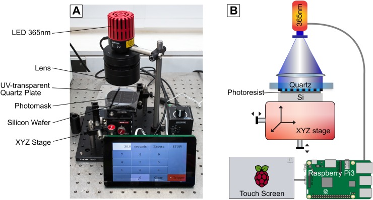
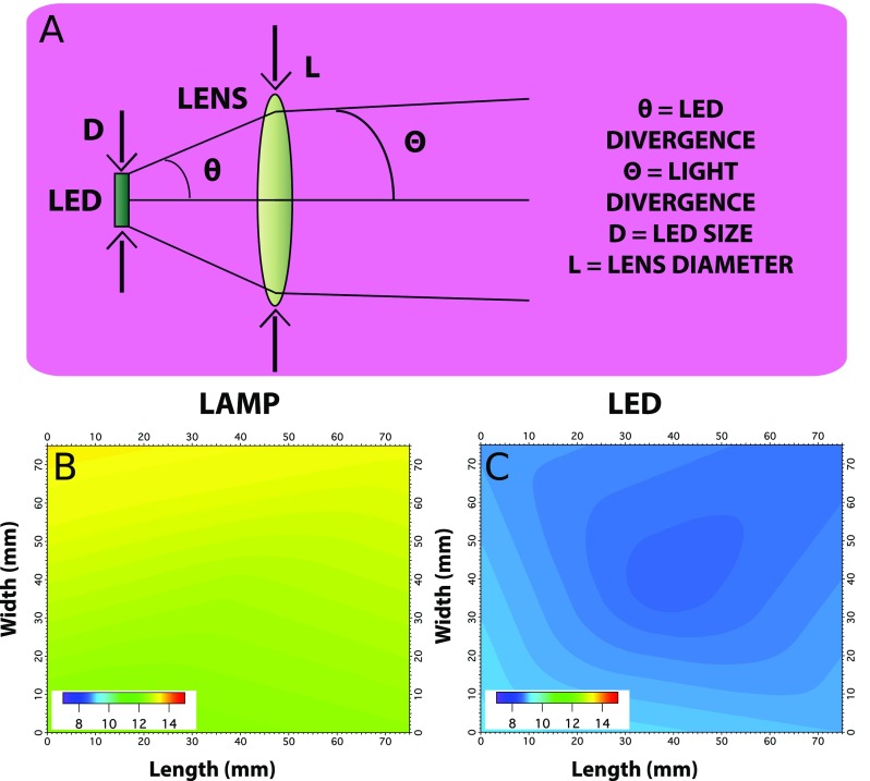
The UV-LED (Thorlabs M365LP1) outputs the maximum power of about 1000 mW when driven by a LED Driver (Thorlabs LEDD1B) set on an external trigger mode supplied with a constant current of 1.2 A. The LED is triggered by a general purpose input/output (GPIO) pin from a Raspberry Pi 3 single board computer, connected to a 7 in. Touchscreen Monitor for user input and control (see Fig. 1 for details). A custom python based graphical user interface (GUI) was developed that allows the user to change the exposure time and start the illumination. An emergency stop button was also included. Even though Python is not a real-time programming language, variability in the timing of the order of 1 ms characteristic of such systems does not represent an issue for exposure times in the range of seconds. In the platform, the LED is positioned 210 mm from the bottom exposure area (table level) and the lens is positioned 60 mm from the LED (Fig. 1). For single layer patterning, when no alignment is necessary, the wafer is positioned on the bottom exposure plane, but it is mounted on the 90 mm high mask aligner when relative alignment of multiple features is necessary. To ensure good resolution, it is crucial that the beam is collimated. In order to collimate the diverging light from the LED, we use an aspheric condenser lens of focal length 60 mm (Thorlabs ACL7560U) as shown in Fig. 2(a). Geometric constraints imply that the divergence angle of light after the lens Θ can be approximated by the relation Θ = θD/L, where D is the size of the LED active area, θ is the LED divergence angle, and L is the diameter of the collimating lens. This factor plays a role in the level of collimation that affects the resolution of the exposure system. For our platform, this value [0.023 rad] is comparable with commercial gas discharge mercury lamp based photolithography systems.
FIG. 1.
Description of the system. (a) Photograph of the UV-LED lithography platform describing the main components used in the platform. (b) Schematic of the Optical and electronic set-up.
FIG. 2.
(a) Figure illustrates the divergence angle of the LED after the collimating lens, (b) 2D map of lamp intensity, and (c) 2D map of LED intensity at the wafer surface for a fixed height of 15 cm from the platforms.
In order to characterise the uniformity of the illumination on a waver scale, we measured the intensity using a detector (Thorlabs S401C) connected to a power meter (Thorlabs PM100A). The power of the light source is an important parameter, which defines the radiation dose that the photoresist is exposed to. Irradiance, the light energy at the wafer surface, has to be calculated to optimise the curing conditions and the light source has thus in general to be calibrated to achieve reproducible results. In the case of a mercury lamp, the intensity decreases over the life time of the lamp whereas it remains appreciably constant for a LED. Upon calibration of our system—using the maximum power of the LED driver—we have evaluated the uniformity of the beam by positioning the detector over the active exposure area (approximately 100 mm2) and compared the results with a conventional mercury lamp (Optical Associated Inc., 200 W NUV). Figures 2(b) and 2(c) show the power map (measured in mW) obtained on the active area. In this case, the detector was 150 mm away from the light source. Our results show that the uniformity in the irradiance is comparable between the LED system and the commercial mercury vapour based system. In particular, the exposure area achieved using our approach is sufficient to uniformly expose a standard 3 in. wafer. The collimation of the beam was also checked by measuring the beam diameter at different heights (40 and 80 mm from the table level) and no major differences were observed.
B. Mask aligner
To allow the use of the exposure source for multi-layer lithography, we combine it with a mask aligner. The mask aligner consists of micrometric XYZ and rotation stages and a holder for a quartz window as shown in Fig. 3(a). The mask alignment procedure consists of 4 steps (Figs. 3(a)–3(c)), described below:
-
1.
Positioning of the wafer on the micrometer stage. The wafer is held in place at the centre of the stage using vacuum grease.
-
2.
Placement of the mask on the wafer. The acetate mask with the features to be transferred is taped to the quartz window. The window is brought into contact with the wafer by sliding it along the vertical posts. The window is clamped into place. Note, for higher resolution features, a chrome mask could also be used instead of the acetate mask tapped onto a quartz window.
-
3.
Positioning of the mask on the wafer. The micrometer stage is brought down (Z-axis) so that the mask is not in contact with the wafer any more and the XY and rotation stages are adjusted to align the registrations marks. The positioning takes place under a binocular. Once the alignment is satisfactory, the Z-stage is brought back up into contact with the quartz window.
-
4.
Exposure. Once the alignment steps are completed, the mask aligner is brought under the UV-LED for exposure. After exposure, the Z-stage is brought back down and the quartz window is removed to release the wafer. The vacuum grease is removed from under the wafer before further processing.
FIG. 3.
Schematic of the mask aligner for lab-scale exposure system and the alignment process. Mask alignment steps to make multilayer devices: (a) Silicon wafer with cured structures and alignment marks is attached onto the XYZ, θ stage, (b) alignment marks on photomask attached to quartz plate are aligned by adjusting the translating and rotation knobs of the XYZ, θ stage, and (c) expose the wafer with UV-LED light.
III. CHARACTERISATION OF THE SET-UP
In this section, we discuss the characterisation of the set-up and show that the features obtained compare well with those obtained using a conventional mercury lamp, but with the advantages of low-cost, convenient and reliable operation characteristic of LED sources. To validate the performance of the UV-LED lithography platform, we have micro-fabricated structures into the negative SU8 3000 series(Microchem) i-line photoresist. The photoresist is spun onto a silicon wafer and soft baked according to the manufacturer's protocols. The photomask with the desired patterns is then placed on the wafer and the whole assembly is positioned under our home built LED-lithography platform. Upon exposure, the UV light crosslinks the exposed SU8 photoresist and the unexposed SU8 is dissolved using appropriate solvents during the development step. After the post exposure bake, the SU8 patterns are visible on the wafer. The patterns obtained using our set-up were examined using a Scanning Electron Microscope and compared with patterns generated using a gas discharge mercury lamp.
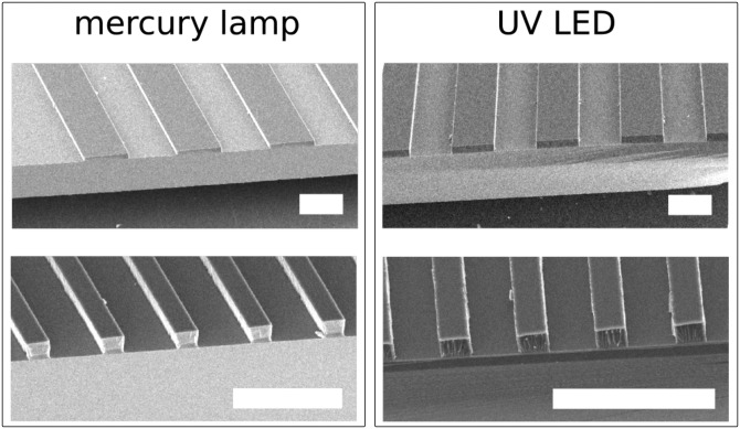
LEDs present a range of advantages compared to mercury lamps. One of them is the stability of the light it produces. Owing to the very nature of mercury lamps—high current intensities degrade the electrode—the intensity of the emitted light decreases over time and as such the lamp should be calibrated regularly. There are a number of specific factors that influence the resolution of the photolithography process. Resolution of features formed through exposure through acetate film masks is commonly limited by the resolution of the printing of the masks themselves, which is commonly of the order of 5–10 μm. However, this can be improved by the use of chrome masks provided the application requires better resolutions. The level of collimation of the light source plays a key role in the resolution of an exposure system. For our system, assuming the feature size of the mask to be S, then the change in size ΔS due to the level of collimation is given by ΔS = , where d is the distance between wafer and mask and Θ is the divergence angle of the light. For our system, the values are 1 μm and 4 μm for resist thicknesses of 25 μm and 100 μm, respectively. These are the typical values that are obtained with lamp based systems. Figure 4 shows a comparison between structures obtained using a mercury lamp and an LED. Observation of the micrographs reveals that the structures (100 μm and 20 μm wide channels of 20 μm height) are comparable.
FIG. 4.
Comparison of SU8 structures obtained using a conventional mercury lamp and a LED. The SEM micrographs show channels (100 μm and 20 μm wide of 20 μm height) fabricated using each light source. The scale bar is 100 μm.
The resolution of the printing on the acetate mask is visible at these scales through slight corrugations in the sides of the channels, both in the UV-LED exposed devices and the ones produced using conventional mercury lamp illumination. Channels with higher resolutions could be obtained using high-resolution chrome mask. The features in the bottom left panel of Fig. 4 are typical of under exposure on the 20 μm wide channels. In particular, it can be seen that the channels are wider at the top of the structure than at the bottom. This image reveals that the mercury lamp used for the experiment needs calibration as its intensity has decreased significantly since the last time it was calibrated. On the other hand, an LED, whose output is largely constant throughout its lifetime, does not require frequent calibration. It can therefore be expected that, under the same conditions, we will obtain more readily the vertical wall structures observed in Fig. 4 with the UV LED set-up.
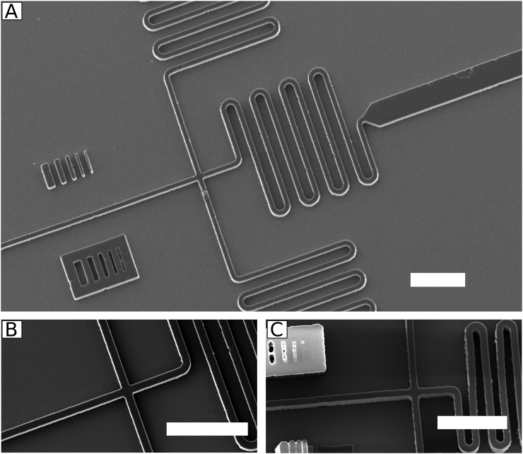
Figure 5 shows typical SU8 structures of droplet maker devices (see Refs. 10 and 11) for examples of experiments exploiting this technology) obtained with the UV LED set-up. Structures of 25 μm height, obtained using a 21 s exposure at full power, are shown in Figs. 5(a) and 5(b). It can be seen that the structures are well resolved in this case and compare well with features obtained using conventional mercury lamps (see Fig. 4). In order to verify the efficiency of the system, we have tested high aspect ratio structures. Channels of 20 μm width and 100 μm height can be seen in Fig. 5(c). In this case, a 40 s exposure time at full power was necessary to obtain well resolved features. Shorter exposure time (and hence a lower UV dose) resulted in a thinner structure that collapsed under their own weight (not shown). If SU8 is underexposed, it is slightly softer12 and, therefore, the structure may collapse. The hard baking time has to be longer than usual to attain a reasonable strength. The height of the 100 μm channels is best seen from the collapsed evaluation feature at the bottom of the image.
FIG. 5.
Evaluation of SU8 features obtained using the UV LED. The scale bar of the SEM micrographs is 200 μm. (a) Structures of 25 μm height obtained after a 21 s exposure time at full power. (b) Details of the structures shown in (a). (c) High aspect ratio structures (100 μm high, 20 μm wide) obtained after a 40 s exposure time at full power.
IV. MICROFLUIDIC DEVICES
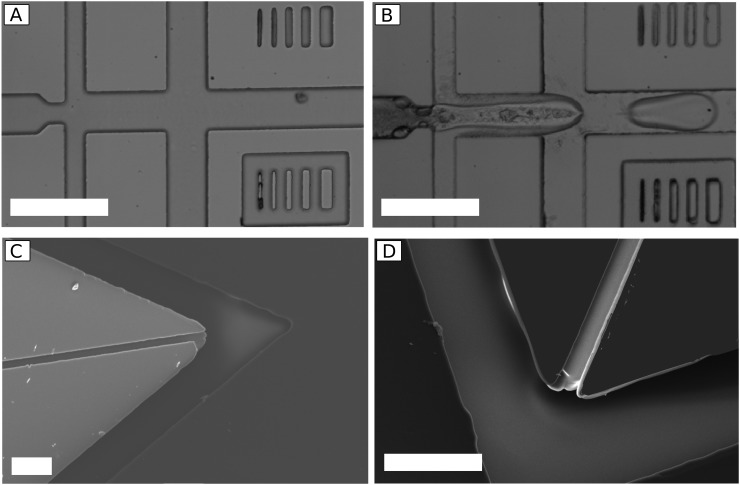
We have designed a double junction droplet maker shown in Fig. 6(a) to demonstrate the functionality of the PDMS cast devices made with the SU-8 masters fabricated using our set-up. The microfluidic channels were treated with Aquapel (PPG Industries) by filling the channels with the solution as received and subsequently washing them with isopropanol prior to the experiments to remove the debris. The treatment improved the wetting of the channels with fluorinated oil.13 Ethanol and water solutions were mixed on the chip to form a solution of 10% (v/v) ethanol in water, and microdroplets were formed in an oil phase of Fluorinert FC-40 (Sigma-Aldrich) and 2.0% (w/w) block-copolymer surfactant. Such a two component mixer on chip devices has been previously used to study peptide self-assembly.14,15 Fig. 6(b) shows the droplet maker while in operation and the two phase mixing within the droplet. As a second example, we have fabricated a non-planar microfluidic device with a 3D junction. By exploiting the alignment procedure described above, we fabricated two layer lithography masters for the replication of PDMS devices. Figures 6(c) and 6(d) show an example of a PDMS replica layer obtained from a master fabricated using a two mask process. The first side of a two-layer 3D flow focusing device is in nature very similar to devices that have been previously used to produce double emulsion droplets.13 The micrograph (Figs. 6(c) and 6(d)) shows that the thin (20 μm wide, 25 μm high) channel is well positioned with respect to the thick channels (50 μm wide, 50 μm high). The rugged edges seen on the PDMS replica are due to the low resolution of the acetate masks. Additional irregularities can be due to the fact that we have a 2-layer master. In this case, it is more difficult to remove uncured photoresists (from the second layer) during the development step. This situation is clearly seen at the intersection between the small and large channels in (Fig. 6(d)). It can also be observed with conventional mask aligners/lamps. In addition, such variations do not affect significantly the performance of the microfluidic device in the cases presented since we are operating in a laminar regime. In case an application requires higher resolution channels, a high-resolution mask should be chosen. Taken together, these results demonstrate the potential of our LED exposure system for single and double layer UV lithography.
FIG. 6.
[Top] Optical Microscope images of double junction droplet maker device and [Bottom] SEM micrographs of features obtained using a two layer photolithography process. (a) Image of droplet maker device, (b) water-ethanol droplets were formed using a block-copolymer surfactant, (c) and (d) show PDMS replica of well aligned channels obtained using the alignment procedure detailed in the paper. The scale bar is 100 μm.
V. CONCLUSIONS
Photolithography, a common patterning technique used in microfabrication, traditionally relies on the use of gas discharge mercury lamps with limited reliability and lifetime. In this paper, we have presented a simple and robust photolithography set-up, comprised of a UV-LED platform with micrometric positioning stages. The resolution of the features obtained by the platform matches that of those required for microfluidics applications. In addition, the system does not suffer from the drawback of conventional gas discharge lamps used in mask aligners that need frequent calibration. The use of LEDs allows for a robust and reliable processing. The alignment procedure presented here by using a combination of micrometric positioning stage was used to produce 2-layer masters. Using soft-lithography, we have reproduced the negative features into PDMS and shown that the devices compare well with devices obtained using a conventional mercury lamp and mask aligner. In summary, LED exposure platforms have the potential to provide the basis for reliable, robust micrometer size lithography applications.
ACKNOWLEDGMENTS
This work was supported by the ERC, the BBSRC, the EPSRC, the Welcome Trust and the Newman Foundation.
Note: The contents of this paper were initially presented at the 8th International Symposium on Microchemistry and Microsystems (ISMM2016).
References
- 1. Bryzek J., Peterson K., and McCulley W., IEEE Spectrum , 20 (1994). 10.1109/6.278394 [DOI] [Google Scholar]
- 2. Barrett C. R., MRS Bull. , 3 (1993). 10.1557/S0883769400037453 [DOI] [Google Scholar]
- 3. Xia Y. and Whitesides G. M., Annu. Rev. Mater. Sci. , 153 (1998). 10.1146/annurev.matsci.28.1.153 [DOI] [Google Scholar]
- 4. Duffy D. C., McDonald J. C., Schueller O. J. A., and Whitesides G. M., Anal. Chem. , 4974 (1998). 10.1021/ac980656z [DOI] [PubMed] [Google Scholar]
- 5. Xia Y. and Whitesides G. M., Angew. Chem. Int. Ed. , 550 (1998). [DOI] [PubMed] [Google Scholar]
- 6. Yapici M. K. and Farhat I., Proc. SPIE , 90521T (2014). 10.1117/12.2046123 [DOI] [Google Scholar]
- 7. Huntington M. D. and Odom T. W., Small , 3144 (2011). 10.1002/smll.201101209 [DOI] [PubMed] [Google Scholar]
- 8. Guijt R. M. and Breadmore M. C., Lab Chip , 1402 (2008). 10.1039/b800465j [DOI] [PubMed] [Google Scholar]
- 9. Suzuki S. and Matsumoto Y., Microsyst. Technol. , 1291 (2008). 10.1007/s00542-007-0544-5 [DOI] [Google Scholar]
- 10. Mashaghi S., Abbaspourrad A., Weitz D. A., and van Oijen A. M., TrAC Trends Anal. Chem. , 118 (2016). 10.1016/j.trac.2016.05.019 [DOI] [Google Scholar]
- 11. Knowles T. P. J., White D. A., Abate A. R., Agresti J. J., Cohen S. I. A., Sperling R. A., De Genst E. J., Dobson C. M., and Weitz D. A., Proc. Natl. Acad. Sci. , 14746 (2011). 10.1073/pnas.1105555108 [DOI] [PMC free article] [PubMed] [Google Scholar]
- 12. Chan-Park M. B., Zhang J., Yan Y., and Yue C., Sens. Actuators, B , 175 (2004). 10.1016/j.snb.2004.02.049 [DOI] [Google Scholar]
- 13. Koster S., Angile F. E., Duan H., Agresti J. J., Wintner A., Schmitz C., Rowat A. C., Merten C. A., Pisignano D., Griffiths A. D., and Weitz D. A., Lab Chip , 1110 (2008). 10.1039/b802941e [DOI] [PubMed] [Google Scholar]
- 14. Levin A., Michaels T. C. T., Adler-Abramovich L., Mason T. O., Muller T., Zhang B., Mahadevan L., Gazit E., and Knowles T. P. J., Nat. Phys. , 926 (2016). 10.1038/nphys3808 [DOI] [Google Scholar]
- 15. Levin A., Mason T. O., Adler-Abramovich L., Buell A. K., Meisl G., Galvagnion C., Bram Y., Stratford S. A., Dobson C. M., Knowles T. P. J., and Gazit E., Nat. Commun. , 5219 EP (2014). 10.1038/ncomms6219 [DOI] [PubMed] [Google Scholar]


