Abstract
Complementary power field effect transistors (FETs) based on wide bandgap materials not only provide high-voltage switching capability with the reduction of on-resistance and switching losses, but also enable a smart inverter system by the dramatic simplification of external circuits. However, p-channel power FETs with equivalent performance to those of n-channel FETs are not obtained in any wide bandgap material other than diamond. Here we show that a breakdown voltage of more than 1600 V has been obtained in a diamond metal-oxide-semiconductor (MOS) FET with a p-channel based on a two-dimensional hole gas (2DHG). Atomic layer deposited (ALD) Al2O3 induces the 2DHG ubiquitously on a hydrogen-terminated (C-H) diamond surface and also acts as both gate insulator and passivation layer. The high voltage performance is equivalent to that of state-of-the-art SiC planar n-channel FETs and AlGaN/GaN FETs. The drain current density in the on-state is also comparable to that of these two FETs with similar device size and VB.
In an ideal inverter system (Fig. 1) for next-generation power conversion systems, a combination of n-channel and p-channel power field-effect transistors (FETs) with equivalent power switching performance is required to achieve complementary operation for power compact systems such as simple gate drive circuits. Diamond, in addition to having the highest reported breakdown field and thermal conductivity, also has the highest hole mobility1, the highest p-type conductivity2,3 and a two-dimensional hole gas (2DHG)4 that makes it a unique and fascinating p-channel material for complementary inverter applications (Fig. 1). In wide bandgap semiconductors, such as III-nitrides, p-type conductivity is much less prevalent than n-type conductivity. The superior p-type nature of diamond enables its use in p-channel FETs; the highest drain current density was reported in wide bandgap p-channel FETs at more than 1 A/mm5 and an on-resistance of 4 Ωmm at a submicron gate length that is comparable to that of n-channel AlGaN/GaN FETs6, because the surface density of the 2DHG is as high as 1012,13 cm−2 7,8. The 2DHG appears where there is a hydrogen-terminated (C-H) diamond surface that has appropriate adsorbates9,10 or film coatings9 to induce holes (Supplementary Fig. S1).
Figure 1. System of complementary wide bandgap semiconductor devices such as that used for power inverters, where the source potentials of the n-channel FETs in the lower arm and the p-channel FETs in the upper arm are fixed at ground level and at a high level, respectively.
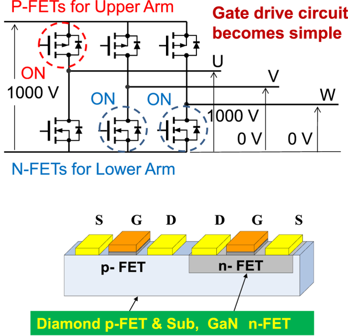
This is an almost ideal circuit and is much simpler than that used in current inverter circuits, in which n-channel FETs are used in both the upper and lower arms, and the source potential in the upper arm is not fixed and thus must be changed by on-off switching. An extra gate drive circuit is needed in the current inverter circuit to apply the appropriate gate-source voltage, but is not required in the complementary system shown.
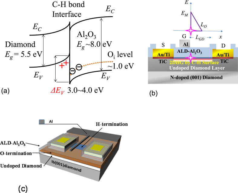
The reliability of C-H diamond FETs has been improved by the passivation11,12 of the adsorbates on C-H diamond by Al2O3 atomic layer deposition (ALD). Recently, the high-temperature stability of a 2DHG13 was reported after ALD of Al2O3 at 450 °C on a cleaned C-H diamond surface by in situ removal of the adsorbates immediately before the ALD process. The 2DHG is generated by the ALD Al2O3 itself, and not necessarily by the adsorbates. The ALD Al2O3 film induces hole accumulation on the n-type Si (n-Si) surface, i.e., a p-type inversion layer14 is produced by the negative charging (electron occupation) of Al2O3 near its interface with n-Si. At the C-H diamond surface, hole accumulation is caused by the negative charging of unoccupied levels such as the interstitial oxygen point defects Oi15,16 or the aluminium vacancies VAL15. These levels are located below the C-H diamond valence band edge, as shown in Fig. 2a. The Oi level (unoccupied states) is located 1.0 eV16 above the valence band edge and the valence band offsets between C-H diamond and Al2O3 are 2.9 eV17 and 3.9 eV18, respectively. When the Oi states near the interface are occupied by electrons with a density of more than 1012 cm−2, 2DHG formation with an equivalent hole density near the interface in C-H diamond satisfies the charge neutrality condition.
Figure 2.
(a) Energy band diagram of interface between Al2O3 and H-terminated (C-H) diamond. The band offset at the valence band edge is 3.0–4.0 eV17,18. Oi is the unoccupied energy level of the interstitial oxygen located at 1.0 eV from the valence band edge of Al2O3. Oi is negatively charged and holes thus accumulate at the C-H diamond surface. (b) Cross-sectional and (c) 3D structure representations of C-H diamond FET with 200-nm-thick Al2O3 gate insulator and drift passivation layer with an asymmetric source and drain structure, where the gate-drain distance LGD was varied from 1 μm up to 25 μm. Electric field distribution along the Al2O3/C-H diamond interface is schematically shown in (b), where a cross symbol indicates the point of the highest electric field on the diamond side.
Using the high temperature (450 °C) ALD Al2O3 as gate oxide and passivation of gate-drain region (drift region), a C-H diamond metal oxide semiconductor (MOS) FET was uniquely designed for high-voltage and high-temperature operation. It is shown schematically as a cross-sectional structure in Fig. 2b and as a 3D image in Fig. 2c. The MOSFET shows clear pinch-off and saturation characteristics with a high on-off ratio in the temperature range from −263 °C (10 K) to 400 °C (673 K) (Supplementary Figs S2 and S3).
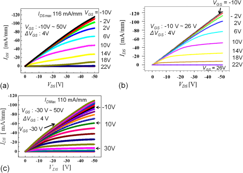
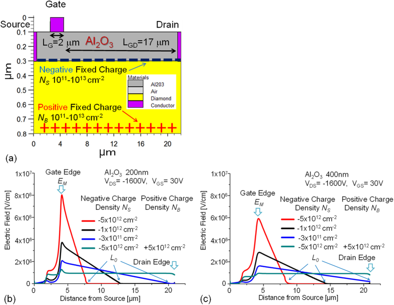
We consider two typical MOSFETs, which both have Al2O3 gates; the first has a passivation oxide thickness of 200 nm, a gate length (LG) of 2 μm, a source-gate distance (LSG) of 2 μm and a gate-drain distance (LGD) of 17 μm, while the second has an oxide thickness of 400 nm, an LG of 9 μm, an LSG of 3 μm and an LGD of 16 μm, and their maximum drain current densities (IDS) were 116 mA/mm and 110 mA/mm, according to their IDS-VDS characteristics (Fig. 3a and c), respectively. The two MOSFETs exhibited breakdown voltages (VB) of 1538 V and 1662 V (Fig. 4a, Fig. 5), respectively. Using a device simulation based on the two-dimensional negatively charged sheet model (Fig. 2a, Fig. 6a, Supplementary Fig. S4), the IDS-VDS characteristics shown in Fig. 3a were reproduced almost exactly in terms of their VGS dependence in Fig. 3b using a negative charge areal density (NS) of 5 × 10¹² e cm−2 with a hole channel mobility of 80 cm2V−1 s−1 at the Al2O3/C-H diamond interface. In general, the charge sheet model is successful in reproducing the characteristics of an AlGaN/GaN FET, where the interface polarization produces the positive charge sheet that is responsible for the two-dimensional electron gas. At the Al2O3/C-H diamond interface, a 2DHG might be formed by the negatively charged sites near the interface as shown in Fig. 2a.
Figure 3. IDS-VDS characteristics at low drain bias and various gate voltages for a diamond FET with breakdown voltages of 1538 V and 1662 V.
Saturation behaviour is observed at VGS > 0 V and pinch-off is obtained at VGS = 30 V. (a) LG = 2 μm, LGD = 17 μm, and oxide thickness of 200 nm, (b) Simulation of (a); (c) LG = 9 μm, LGD = 16 μm, and oxide thickness of 400 nm.
Figure 4. Logarithmic ID-VDS characteristics showing the blocking behaviour of C-H diamond MOSFETs with a common gate width (25 μm) in the off-state for various LGD values of 9, 16, 17, 20 and 22 μm.
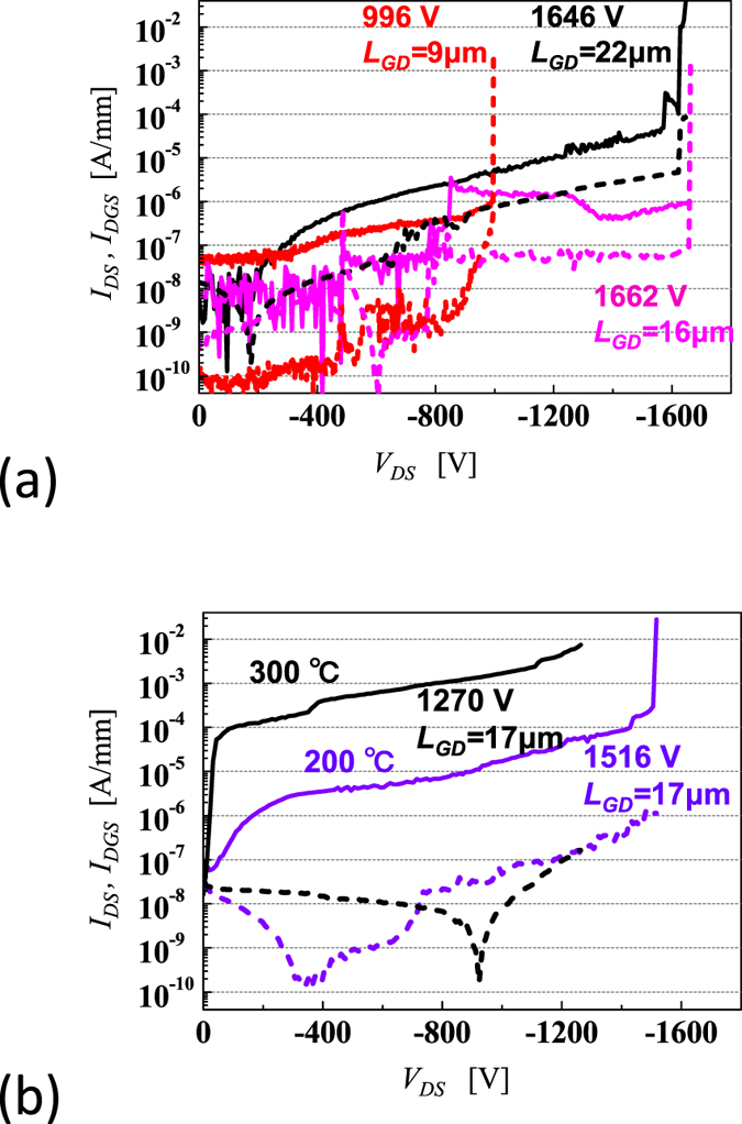
Solid lines represent the source-drain current (IDS) and dotted lines represent the source-gate-drain current (IDGS).(a) For LGD values of 9, 16, and 22 μm, the breakdown voltages are VB = 996, 1662, and 1646 V at room temperature, respectively. (b) For LGD of 17 μm, the breakdown voltages are VB = 1516 and 1270 V at 200 °C and 300 °C, respectively.
Figure 5. Maximum breakdown voltage (VB) as a function of gate-drain length (LGD).
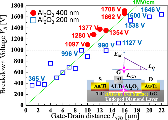
The MOSFETs are composed of a 200-nm-thick Al2O3 layer as the gate insulator and 200- or 400-nm-thick Al2O3 layers acting as a passivation layer between the gate metal and drain metal. VGS for the off-states are +20- + 60 V.
Figure 6.
(a) Simulation model for a MOSFET displaying the IDS-VDS characteristics shown in Fig. 3a. A MOS structure is composed of metal, Al2O3 and undoped diamond. Source and drain metals contact with the undoped diamond at both edges with 0 eV Schottky barrier height. Negative and positive charge sheets are spaced at the Al2O3/diamond interface and at the bottom of undoped diamond, respectively. (b) Electric field distributions along the Al2O3/C-H diamond interface that were calculated using the model shown in (a), where the Al2O3 thickness is 200 nm. (c) The same electric field distributions, calculated when the Al2O3 thickness is 400 nm.
The off-state characteristics before breakdown of the diamond MOSFETs of Al2O3 (mostly 200 nm in thickness) with a common gate width (25 μm) and different gate-drain length (LGD) values of 9, 16, 17, and 22 μm were investigated at room temperature (RT) and at higher temperatures until breakdown started to occur, and the results are shown in Fig. 4. VGS for the off-states are +20- + 60 V. The maximum VB at each LGD are 996 V (LGD = 9 μm), 1270 V (20 μm, 300 °C), 1512 V (17 μm, 200 °C), 1646 V (22 μm), and 1662 V (16 μm, with a thicker oxide layer of 400 nm). The source-drain current (drain leakage current) IDS gradually increases at higher temperatures. At 800 V, the leakage currents at room temperature range from 2 × 10⁻⁷ to 5 × 10⁻⁶ A/mm (Fig. 4a) and the corresponding values at 200 and 300 °C are 8 × 10⁻⁶ A/mm and 10−3 A/mm (Fig. 4b), respectively. In general, the drain leakage current increases gradually at a high voltage (high electric field) and breakdown starts to occur. These values are acceptable for power device applications. In contrast, the source-gate-drain current (or gate leakage current) IDGS is one to two orders of magnitude less than IDS, as shown in Fig. 4. At the start of the breakdown process, when IDGS reaches IDS, gate-drain breakdown through the gate oxide may be a main cause. One such example is a FET with LGD = 9 μm and VB = 996 V (see Fig. 4a). In other cases, however, IDGS is less than IDS by more than an order of magnitude at breakdown. Most breakdown processes are initiated at the drift region near the gate.
The maximum breakdown voltage VB at each LGD is shown in Fig. 5 with two different passivation thicknesses (200 nm and 400 nm). When LGD is 1 μm, VB = 365 V is obtained (Supplementary Fig. S5). For a short LGD of 1 μm, the punch-through condition (under which the difference between the electric fields along the Al2O3 /C-H diamond interface on the gate and drain sides is small) has been applied based on the electric field distribution that can be calculated via device simulations, as discussed later in this work. The averaged electric field is simply calculated to be VB/LGD = 3.6 MV/cm. This value is equivalent to that of the breakdown fields of SiC and GaN. As LGD increases to 9 μm, VB also increases and reaches 996 V at LGD = 9μm. As LGD increases further, VB also increases correspondingly until LGD = 22 μm. VB values of 1600 V and 1646 V are obtained at LGD = 20 and 22 μm (Fig. 5), respectively. With a thicker (400 nm) Al2O3 passivation layer between the gate and the drain, VB values from 1097 to 1708 V are obtained from LGD = 11 to 16 μm (Fig. 5). When a thicker oxide layer is used, VB increases above 1000 V up to 1700 V with increasing LGD. The peak electric field at diamond side with thicker passivation layer (400 nm) is decreased by 25–30% compared with that of 200 nm thickness (discussed later). The VB of 1708 V (Supplementary Fig. S6) is the highest value ever reported for a diamond FET with on-state IDS~100 mA/mm, and is comparable to that of SiC19 or AlGaN/GaN20,21 FETs with similar LGD (Table 1).
Table 1. Comparison of maximum breakdown voltages VB Max and maximum drain current density ID Max at a particular LGD less than 20 μm in planar FETs of SiC, AlGaN/GaN, AlGaN/AlGaN, and diamond.
| Wide Bandgap Planar FETs | VB MAXBreakdow Voltage | LGD Gate Drain Distance | VB/LGDBreakdown Field | ID MAXDrain Current Density |
|---|---|---|---|---|
| SiC n-FET19 | 1600 V | 20 μm | 0.8 MV/cm | 90 mA/mm |
| AlGaN/GaN20,21 n-FET | 1500 V | 15 μm | 1.0 MV/cm | 300-600 mA/mm |
| AlGaN/AlGaN22 n-FET | 1700 V | 10 μm | 1.7 MV/cm | 200 mA/mm |
| C-H Diamond p-FET | 1700 V | 16 μm | 1.0 MV/cm | 110 mA/mm |
In the off-state of the MOSFET with the two-dimensional negative charge sheet (Fig. 2a, Fig. 6a), the electric field along the Al2O3/C-H diamond interface in the lateral direction contains a peak that occurs near the gate edge, as indicated by the cross shown in Fig. 2b, with a maximum value denoted by EM. The electric field along the Al2O3/diamond interface decreases with increasing distance from the gate edge, and almost reaches zero at a distance L0 from the gate edge. The electric field distribution along the Al2O3/diamond interface is evaluated using MOSFET device simulations with various densities (NS) of the 2D negative charges (1 × 1011 × 1013 cm−2) that were distributed homogeneously at the Al2O3/C-H diamond interface (Fig. 6a). In Fig. 6b and c, along the Al2O3/diamond interface, several of the electric field distributions that are responsible for VDS = 1600 V are shown for various NS. The reason why VDS = 1600 V was selected as an example here is that it is approximately equal to the frequently observed value of the highest operating voltage that is available in FETs at present. The VGS for the off-state is maintained at 30 V, so the gate-drain voltage drop is higher than the source-drain voltage drop. However, the gate potential does not have a major effect on the electric field or the potential distribution between the source and the drain. EM is effectively reduced by the thicker Al2O3 (400-nm-thick) layer at each NS. At NS = 5 × 1012 cm−2, which reproduces an experimental IDS-VDS characteristic in the on-state (Fig. 3a and b), the EM and L0 values with the 200-nm-thick Al2O3 layer are calculated to be 8.1 MV/cm and 3.5 μm at VDS = 1600 V (Fig. 6b), respectively. The corresponding values when using a 400-nm-thick Al2O3 layer are calculated to be 5.9 MV/cm and 4.5 μm at 1600 V, respectively (Fig. 6c). Because the voltage drop of 1600 V occurs within the calculated L0 (<5 μm), MOSFETs with VB ~1600 V are expected to be realized at an LGD of just over 5 μm, but are actually obtained experimentally at LGD > 16 μm (Fig. 5). This inconsistent result indicates that that the real value of L0 is greater and the real EM is smaller than the values calculated based on NS = 5 × 1012 cm−2. It is reasonable that the effective value of NS is much lower than 5 × 1012 cm−2. At NS = 3 × 1011 cm−2, L0 reaches 16 μm, as shown in Fig. 6b and c. The fact that VB ~1600 V is obtained at an LGD of more than 16 μm indicates that NS < 3 × 1011 cm−2. As shown in Fig. 5, the maximum value of VB is roughly proportional to LGD. This behaviour may also be caused by a lower effective charge density, such as NS < 3 × 1011 cm−2.
The original negative charge density can be either reduced or cancelled in one of two main ways. The first involves hole injection into the Al2O3 layer on an undoped diamond layer. Energetic (hot) holes that are accelerated by a high electric field can enter the Al2O3 layer beyond the large band offset between the Al2O3 layer and C-H diamond (2.9–3.9 eV) (Fig. 2a)17,18. This effect on the electric field distribution can also be simulated using smaller NS values such as NS = 1 × 10¹² and 3 × 1011 cm−2, as shown in Fig. 6b and c. The other way involves use of positively ionized nitrogen donors in a nitrogen-doped diamond substrate (nitrogen concentration of 1019 cm−3) under the undoped diamond layer (Fig. 2b). Substitutional nitrogen atoms that act as deep donors can be positively ionized via hole recombination with an electron from a neutral nitrogen donor. The deep donor level (1.7 eV) means that this positive charge can be maintained for a long time because of the very low density of the conduction electrons. The ionized donors are randomly distributed in a nitrogen-doped substrate beneath the undoped layer. For simplicity, we assume here that the donors are distributed as a positive charge sheet with a charge areal density of NB. In the device simulations, it is varied from 1–6 × 1012 cm−2 at the bottom of the undoped diamond (Fig. 6a) and NS is fixed at 5 × 1012 cm−2 (NS0), then NB compensates NS0 to produce NS0 − NB. When NS0 − NB produces values of 1 × 10¹² and 3 × 1011 cm−2, the corresponding electric field distributions (which are not shown here) are calculated to be almost the same as those shown at NS = 1 × 10¹² and 3 × 1011 cm−2 in Fig. 6b and c. When NS0 − NB = 0, perfect charge compensation occurs and the electric field distribution becomes flat, as shown in Fig. 5b and c (indicated by the green lines). This is an ideal situation for high-voltage device structures such as super-junctions. When 1 × 1012 cm−2 > NS0 − NB > −1 × 1012 cm−2. the maximum IDS is preserved at 60–90% of the value obtained by the NS0 (Fig. 3b), indicating that the positively charged embedded layer does not reduce the channel and drift hole conduction so greatly near the surface.
The drain current density (IDS) of the diamond FET with the breakdown voltage of 1538 V and 1662 V exceeds 100 mA/mm, according to the IDS-VDS characteristics at low drain bias shown in Fig. 3. Saturation behaviour is observed at VGS > 0 V and pinch-off is obtained at VGS = 50 V. At VGS < 0 V, the drain current increases and becomes linear. Finally, the drain current does not increase further upon application of a more negative gate bias. The saturated slope of the IDS-VDS characteristic is mainly due to the gate-drain resistance, because it is the main resistive part of the high voltage device. However, the total drain on-current for a source-to-drain distance of 25–30 μm is more than 100 mA/mm, which is comparable to the corresponding currents of SiC lateral MOSFETs (90 mA/mm)19, AlGaN/GaN HFETs (300–600 mA/mm)20,21 and AlGaN/AlGaN HFETs (200 mA/mm)22 with an equivalent device size and VB (Table 1). A higher on-current can be achieved at a lower VDS by increasing either the hole areal density or the sub-surface mobility.
The maximum IDS was investigated as a function of temperature for diamond FETs with the C-H channel (2DHG) and with a boron-doped channel (Fig. 7). The IDS of the C-H channel only changes by approximately 40% from −263 °C to 300 °C. In the C-H channel MOSFETs, which show VB of more than 1000 V, IDS is approximately 20 mA/mm at VDS = 10 V and approximately 100 mA/mm at VDS = 50 V at room temperature. At higher temperatures, IDS decreases slightly because of the reduction in hole mobility caused by phonon scattering. In contrast, the boron-doped channel FETs with a high VB of more than 600 V show a rapid increase in IDS by more than one order of magnitude over the range from room temperature to 200–300 °C. This is caused by the activation of boron as a relatively deep acceptor (0.37 eV), with doping levels of 5 × 10¹⁵ and 1 × 1017 cm−3 in the metal-semiconductor field-effect transistor (MESFET)23 and the junction FET (JFET)24,25, respectively. The drain current densities of the 2DHG channel are more than two orders and one order of magnitude higher than those of the boron-doped channel at room temperature and in 200–300 °C range, respectively.
Figure 7. Temperature dependence of maximum drain current density (IDS) of diamond FETs.
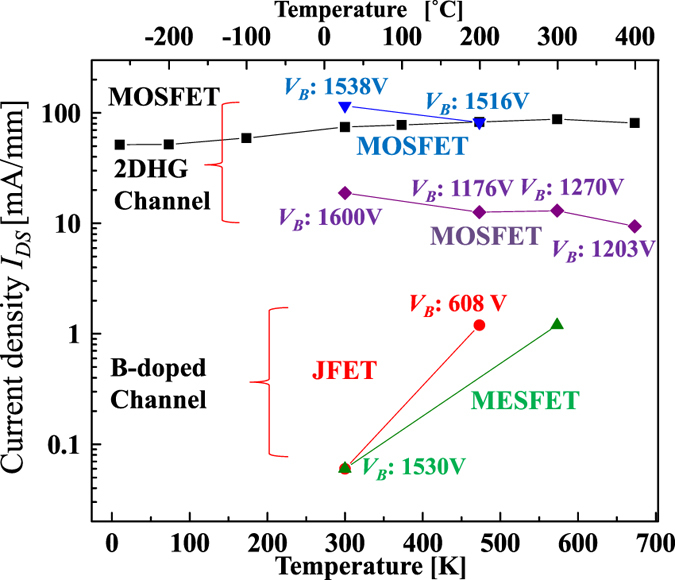
The current density is normalized with respect to the gate width. The temperature dependence of a MOSFET under drain source bias of 10 V and 50 V and that of a junction FET25 and a MESFET23 with a boron-doped channel at VDS = 10 V are also shown.
Junction FETs, including MESFETs, regulate their depletion layer fronts far away from their p-n or MES junctions to control their bulk p-type channel thicknesses. Therefore, the drain current controllability in these FETs is low, but the current is stable because the channel carriers are not affected by the junction charge. Because a MOSFET can control surface band bending, the current response of its gate is efficient, but it is also sensitive to interface charge. The 2DHG that occurs at the Al2O3/C-H diamond interface may originate from the electric field (band bending) that is induced by the negative charges in Al2O3 near the interface and the applied gate voltage. The drain current can be increased or reduced effectively, because the C-H surface has a very low surface state density when compared with that of the C-O surface that is normally used in MESFETs.
High performance 2DHG diamond MOSFETs with submicron gate lengths have already obtained maximum current densities of 1.2–1.3 A/mm5,26, on-resistances of 4–6 Ωmm5, and transconductances of 200–480 mS/mm5. These values are comparable to those of AlGaN/GaN devices of the same size. In the long LGD diamond FETs that are used for high voltage applications, however, the drain current density and the transconductance become more than one order of magnitude lower because of the low mobility (70–100 cm2 V−1 s−1) in the 2DHG drift layer. Mobility enhancement of the 2DHG layer by up to 500 cm2 V−1 s−1 or the discovery of a shallow acceptor with an acceptor level that is lower than 0.2 eV will dramatically improve the specific on-resistance for high voltage applications.
Conclusions
By creation of a 2DHG using a high-temperature ALD Al2O3 layer on a C-H bond diamond surface, the following p-channel MOSFET characteristics have been obtained.
1) Off-state. When LGD increases from 1 μm to 22 μm, VB increases up to roughly 1600 V in the off-state with the increasing LGD. The maximum breakdown voltage is 1700 V at room temperature, 1500 V at 200 °C and 1200 V at 300 °C and 400 °C.
2) On-state. In the high voltage FET with VB of 1600 V, the maximum current density in the on-state when normalized with respect to the channel width is 100 mA/mm and is nearly constant from −200 °C (73 K) to 400 °C (673 K).
These high-voltage breakdown characteristics in the off-state and the drain current density per unit gate width in the on-state are comparable to those characteristics of lateral SiC and III-nitride FETs. Because the 2DHG at the C-H diamond surface is ubiquitous and was stably covered with ALD Al2O3, the above FET performance can easily be transferred to vertical power devices such as trench gate MOSFETs. These results demonstrates the potential for application of a diamond p channel FET as a smart power inverter using complementary power FETs (Fig.1).
Method
The C-H diamond MOSFET for high voltage and high temperature operation is shown schematically as a cross-sectional structure in Fig. 2b and as a 3D image in Fig. 2c. The MOSFET fabrication process without deterioration of the C-H bonds is briefly described in the following. The starting substrate is synthetic diamond (001), which was formed under high-pressure and high-temperature (HPHT) conditions. In this HPHT synthetic diamond, nitrogen atoms are incorporated as deep donors at a concentration of 1019 cm−3. On this substrate, a nominally undoped diamond layer is homoepitaxially grown by microwave plasma-assisted chemical vapour deposition to a thickness of 0.5 μm (Supplementary Fig. S7a). Source and drain metal contacts are then formed by Au/Ti deposition (Supplementary Fig. S7b). Most of the surface area, except for the source and drain contacts, is then H-terminated by remote plasma treatment at 600 °C (Supplementary Fig. S7c). During that time, TiC is formed to erode the diamond layer to a depth of a few nm and subsequently form a stable contact to the diamond. The H-terminations are replaced with O-terminations through a local oxidation process to form an isolated region, and thus an H-terminated channel remains between the source and drain (Supplementary Fig.S7d). Al2O3 is then deposited at 450 °C by ALD to simultaneously form the gate insulator and the passivation layer (Supplementary Fig. S7e). During Al2O3 formation, the conditions required for the 2DHG are satisfied. Finally, the gate metal (Al) is deposited and the gate is patterned using a lift-off process (Fig. 2c, Supplementary Fig. S7f).
Additional Information
How to cite this article: Kawarada, H. et al. Durability-enhanced two-dimensional hole gas of C-H diamond surface for complementary power inverter applications. Sci. Rep. 7, 42368; doi: 10.1038/srep42368 (2017).
Publisher's note: Springer Nature remains neutral with regard to jurisdictional claims in published maps and institutional affiliations.
Supplementary Material
Acknowledgments
This work was supported in part by a Grant-in-Aid for Fundamental Research S (Grant No. 26220903) from the Ministry of Education, Culture, Sports, Science and Technology (MEXT), Japan, and by the Advanced Low Carbon Technology Research & Development Program (ALCA) from the Japan Science and Technology Agency (JST).
Footnotes
The authors declare no competing financial interests.
Author Contributions H.K. conceived the idea. M.I. optimized CVD diamond growth. T.Y., D.X., H.T., Y.K., and T.K. fabricated FETs and measured their characteristics. M.S. performed device simulation, D.M. formed gate insulator and characterized it. A.H. analysed the leakage current through gate insulator of FETs. H.K. wrote the manuscript with the help of all co-authors.
References
- Isberg J. et al. High carrier mobility in single-crystal plasma-deposited diamond. Science 297, 1670–1672 (2002). [DOI] [PubMed] [Google Scholar]
- Ekimov E. et al. Superconductivity in diamond. Nature 428, 542–545 (2004). [DOI] [PubMed] [Google Scholar]
- Yokoya T. et al. Origin of the metallic properties of heavily boron-doped superconducting diamond. Nature 438, 647–650 (2005). [DOI] [PubMed] [Google Scholar]
- Nebel C. E. Chemistry. Surface-conducting diamond. Science 318, 1391–1392 (2007). [DOI] [PubMed] [Google Scholar]
- Kawarada H. High-current metal oxide semiconductor field-effect transistors on H-terminated diamond surfaces and their high-frequency operation. Jpn. J. Appl. Phys. 51, 090111 (2012). [Google Scholar]
- Mishra U. K., Parikh P. & Wu Y. AlGaN/GaN HEMTs-an overview of device operation and applications. PROCEEDINGS-IEEE 90, 1022–1031 (2002). [Google Scholar]
- Kawarada H. Hydrogen-terminated diamond surfaces and interfaces. Surf. Sci. Rep. 26, 205–259 (1996). [Google Scholar]
- Nebel C. et al. Hydrogen-induced transport properties of holes in diamond surface layers. Appl. Phys. Lett. 79, 4541–4543 (2001). [Google Scholar]
- Strobel P., Riedel M., Ristein J. & Ley L. Surface transfer doping of diamond. Nature 430, 439–441 (2004). [DOI] [PubMed] [Google Scholar]
- Chakrapani V. et al. Charge transfer equilibria between diamond and an aqueous oxygen electrochemical redox couple. Science 318, 1424–1430 (2007). [DOI] [PubMed] [Google Scholar]
- Kueck D., Schmidt A., Denisenko A. & Kohn E. Analysis of passivated diamond surface channel FET in dual-gate configuration—Localizing the surface acceptor. Diam. Relat. Mater. 19, 166–170 (2010). [Google Scholar]
- Kasu M., Sato H. & Hirama K. Thermal stabilization of hole channel on H-terminated diamond surface by using atomic-layer-deposited Al2O3 overlayer and its electric properties. Appl. Phys. Express 5, 025701 (2012). [Google Scholar]
- Hiraiwa A., Daicho A., Kurihara S., Yokoyama Y. & Kawarada H. Refractory two-dimensional hole gas on hydrogenated diamond surface, J. Appl. Phys. 112, 124504 (2012). [Google Scholar]
- Werner F. & Schmidt J. Manipulating the negative fixed charge density at the c-Si/Al2O3 interface. Appl. Phys. Lett. 104, 091604 (2014). [Google Scholar]
- Matsunaga K., Tanaka T., Yamamoto T. & Ikuhara Y. First-principles calculations of intrinsic defects in Al2O3. Phys. Rev. B 68, 085110 (2003). [Google Scholar]
- Yang M. Y., Kamiya K. & Shiraishi K. Interstitial oxygen induced Fermi level pinning in the Al2O3-based high-k MISFET with heavy-doped n-type poly-Si gates. AIP Adv. 3, 102113 (2013). [Google Scholar]
- Liu J., Liao M., Imura M. & Koide Y. Band offsets of Al2O3 and HfO2 oxides deposited by atomic layer deposition technique on hydrogenated diamond. Appl. Phys. Lett. 101, 252108 (2012). [Google Scholar]
- Takahashi K., Imamura M., Hirama K. & Kasu M. Electronic states of NO2-exposed H-terminated diamond/Al2O3 heterointerface studied by synchrotron radiation photoemission and X-ray absorption spectroscopy. Appl. Phys. Lett. 104, 072101 (2014). [Google Scholar]
- Noborio M., Suda J. & Kimoto T. 1580-V–40-double-RESURF MOSFETs on 4H-SiC. IEEE Electron Device Lett. 30, 831–833 (2009). [Google Scholar]
- Lu B. & Palacios T. High Breakdown (>1500 V) AlGaN/GaN HEMTs by Substrate-Transfer Technology. IEEE Electron Device Lett. 31, 951–953 (2010). [Google Scholar]
- Lee J. et al. High Breakdown Voltage (1590 V) AlGaN/GaN-on-Si HFETs with Optimized Dual Field Plates (CS MANTECH Conference, April 23rd-26th, 2012).
- Nanjo T. et al. AlGaN channel HEMT with extremely high breakdown voltage. IEEE Trans. Electron Dev. 60, 1046–1053 (2013). [Google Scholar]
- Umezawa H., Matsumoto T. & Shikata S. Diamond metal–semiconductor field-effect transistor with breakdown voltage over 1.5 kV. IEEE Electron Device Lett 35, 1112–1114 (2014). [Google Scholar]
- Iwasaki T. et al. High-temperature operation of diamond junction field-effect transistors with lateral pn junctions. IEEE Electron Device Lett. 34, 1175–1177 (2013). [Google Scholar]
- Iwasaki T. et al. 600 V diamond junction field-effect transistors operated at 200 °C. IEEE Electron Device Lett., 35, 241–243 (2014). [Google Scholar]
- Hirama K., Sato H., Harada Y., Yamamoto H. & Kasu M. Diamond field-effect transistors with 1.3 A/mm drain current density by Al2O3 passivation layer. Japanese Journal of Applied Physics 51, 090112 (2012). [Google Scholar]
Associated Data
This section collects any data citations, data availability statements, or supplementary materials included in this article.


