Abstract
Great efforts have been devoted to achieving efficient Si-based light-emitting devices. Here we report new light-emitting devices fabricated with Tb2O3 on Si substrates. Intense green electroluminescence was observed, with a turn-on voltage of about 8 V. The green emission is attributed to the characteristic transitions of Tb3+ ions in Tb2O3. The electroluminescence mechanisms of the Tb2O3 light-emitting devices are discussed. In addition, visible and near infrared electroluminescence was observed in rare-earth (Eu3+, Sm3+ and Yb3+) doped Tb2O3 light-emitting devices.
Si-based photonics have been regarded as an effective way to improve data transfer rates of information processing systems1. In the past decades, great efforts have been devoted to achieving efficient Si-based light sources2,3,4,5,6. Rare-earth (RE) doped SiO2 has attracted a lot of interest due to their high luminescence efficiency and wide spectral range extending from ultraviolet (UV) to infrared (IR) ranges7,8,9. Previously, efficient visible light-emitting devices (LEDs) based on RE-doped metal-oxide-semiconductor (MOS) structures have been demonstrated10,11,12. However, both the light emission yield and the reliability of the RE-doped oxides devices are limited by charge trapping and RE clustering effects13.
Tb2O3 is a very attractive member of RE oxides since it is a direct and wide-band-gap semiconductor (~3.8 eV), and its lattice constant (~10.73 Å) matches Si (~5.431 Å)14. Haugsrud et al. reported that Ca-doped Tb2O3 is a p-type semiconductor15. In particular, Tb3+ ions have been widely used as ideal activator ions for green display devices, detectors, and lasers16. In these applications, different emission wavelengths have been achieved owing to the energy transfer between Tb3+ and other RE ions (such as Eu3+, Sm3+, Nd3+, Yb3+)17,18,19,20. However, so far, there has been no reports on electroluminescence (EL) of Tb2O3.
Here we demonstrate, for the first time, new green LEDs using Tb2O3 on Si substrates. Tb2O3 thin films were prepared by magnetron sputtering and annealed in an O2 ambient. Strong green emission was observed, with a turn-on voltage of 8 V. EL mechanisms of the Tb2O3 LEDs are also discussed. In addition, intense red, orange, and near IR emissions are obtained from RE3+ (Eu3+, Sm3+ and Yb3+) doped Tb2O3 LEDs on Si substrates, respectively. Our results show that Tb2O3 LEDs can be potentially used in display, optical communication, and other Si-based optoelectronics.
Results and Discussion
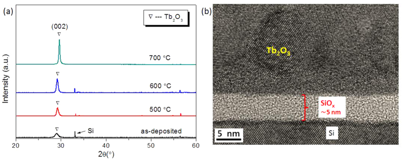
The crystalline phases of as-deposited and annealed Tb2O3 films were investigated by X-ray diffraction (XRD). As shown in Fig. 1(a), the as-deposited film shows a weak diffraction peak at 2θ ≈ 29.0°, which corresponds to (002) plane of hexagonal Tb2O3. This peak increases and narrows with increasing the annealing temperature. Strong peak of (002) plane of Tb2O3 is observed when the annealing temperature is further raised to above 700 °C. The lattice structure of the films is investigated by using a transmission electron microscope (TEM). The high-magnification TEM image shows the presence of crystalline areas in the Tb2O3 film. As shown in Fig. 1(b), there is an amorphous SiOx layer at the Tb2O3/Si interface, with a thickness of about 5 nm.
Figure 1. Lattice structure of the films.
(a) XRD of as-deposited and annealed Tb2O3 films (~200 nm) at 500, 600, and 700 °C for 1 hour, respectively. (b) High-magnification TEM image of a Tb2O3 film.
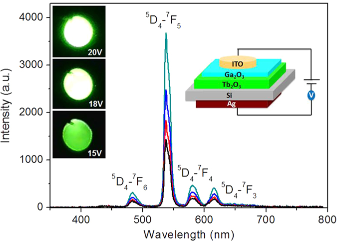
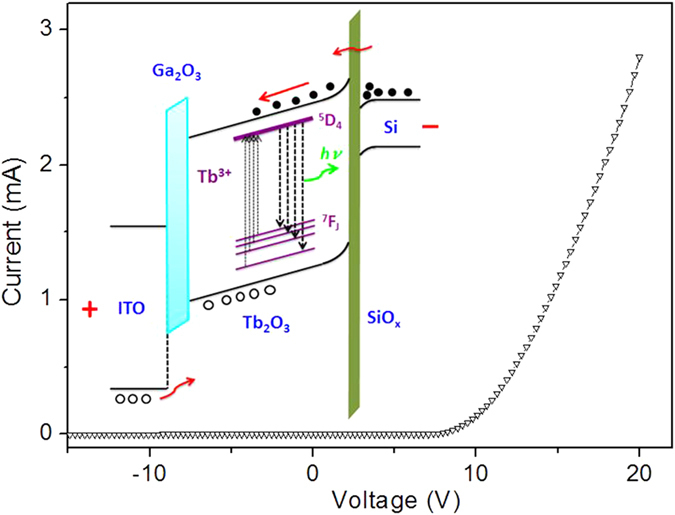
A Tb2O3 LED was fabricated with the structure diagram shown in the inset of Fig. 2. Intense green EL is observed when a positive voltage is applied on the indium tin oxide (ITO) layer, while no EL is detectable under reverse biases. The turn-on voltage of the device is as low as 8 V. The emission is bright enough to be observed by naked eyes under normal room light. The EL spectrum shows peaks at 484, 540, 582, and 616 nm, which correspond to 5D4–7F6, 5D4–7F5, 5D4–7F4, and 5D4–7F3 transitions of Tb3+, respectively16. The 5D4–7F5 transition is the most intense one and features a double-peak structure, which can be attributed tothe crystal field splitting of the ground state. When increasing the forward bias, the EL spectral shape remains unchanged, with the intensity increasing with the applied voltage from 8 V up to 20 V. The forward current of the device reaches 2.8 mA when the forward bias is 20 V, while the reverse leakage current is minimal. These results show that the Tb2O3 LED has excellent rectification performance.
Figure 2. EL performance of the Tb2O3 LED.

EL spectra of the LED at the voltage of 12–20 V, the insets show the structure diagram of the LED and EL photos of the device at different voltages.
The EL mechanism is schematically illustrated in the inset of Fig. 3. When a sufficiently high forward bias is applied, the energy bands of both Tb2O3 and SiOx bend upward along the electric field direction. According to Zhu et al.21,22,23, a trap-assisted tunneling (TAT) mechanism dominates the conduction mechanism at the EL-enabling voltages. When a sufficiently high forward bias voltage is applied between the two electrodes, a large number of electrons in Si accumulate in Si/SiOx interface and then reach the conduction band of Tb2O3 by tunneling through the SiOx barrier. Meanwhile, holes are injected from ITO electrode into the Ga2O3 layer and then enter the Tb2O3. The holes accumulate at Tb2O3/SiOx interface due to the SiOx barrier. Thus, direct impact excitation of Tb3+ ions are exerted when the kinetic energies exceeds the threshold energy.
Figure 3. Electrical characterization of Tb2O3 LED.

Current-voltage characteristic of the device. The inset shows the energy band diagram of the devices and the charge transfer process.
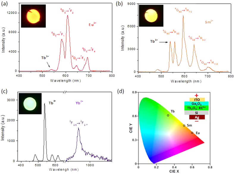
We have demonstrated a bright green EL device based on Tb2O3. To further explore the possibility of using Tb2O3 as a host material to RE ions to achieve devices of other colors, we further fabricated EL devices with RE-doped Tb2O3. Intense red EL is observed from Eu3+ doped Tb2O3 LED. As shown in Fig. 4(a), the emission peaks are at about 582, 619, 646, and 694 nm, corresponding to 5D0–7FJ (J = 1, 2, 3, and 4) transitions of Eu3+. The highest peak at 619 nm corresponds to the Eu3+ electric dipole transitions of 5D0–7F217. In Fig. 4(b), strong orange EL is observed from Sm3+ doped Tb2O3 LED. The characteristic of the 4G5/2–6HJ (J = 5/2, 7/2, 9/2, and 11/2) transitions of Sm3+ ions are appeared. The Sm3+ emission peaks are from transitions of 4G5/2–6H5/2 (558 nm), 4G5/2–6H7/2 (593 nm), 4G5/2–6H9/2 (640 nm), and 4G5/2–6H11/2 (701 nm)18. In Fig. 4(c), both green emission of Tb3+ and near IR emission of Yb3+ are obtained. The characteristic peak of Yb3+ is attributed to the transition from 2F5/2 to 2F7/219. As shown in Fig. 4(d), The CIE coordinates of the green-, red- and orange-emitting devices are (0.33, 0.61), (0.60, 0.39) and (0.51, 0.48), respectively.
Figure 4. EL performance of the LEDs.
(a–c) EL spectra of the red-, orange- and near IR-emitting devices from Eu3+, Sm3+, Yb3+ doped LED at forward biases of 20 V, respectively. (d) CIE coordinates of the green-, red- and orange-emitting devices.
In summary, new LEDs from Si-based Tb2O3 are fabricated. Intense green EL was observed, with a turn-on voltage of about 8 V. The green emission centered at 484, 540, 582, and 616 nm, corresponding to the 5D4–7FJ transitions of Tb3+ in Tb2O3, where J = 6, 5, 4, and 3. The EL intensity increases with the applied voltage up to 20 V. In addition, red, orange, and near infrared EL were observed from RE3+ (Eu3+, Sm3+ and Yb3+) doped Tb2O3 LEDs, respectively. Our results could provide a possible route for achieving stable and highly efficient Si-based LEDs.
Methods
About 200 nm Tb2O3 films and RE-doped Tb2O3 films were deposited on n-type Si (100) substrates by magnetron co-sputtering technique. The Si substrates were cleaned by dipping in a dilute HF solution (HF:H2O = 1:7) for 60 s. Tb (99.95%) target was sputtered in Ar:O2 = 15:5 atmosphere, at a substrate temperature of 150 °C. The deposition rate was 0.4 Å/s. RE ions (RE = Sm, Eu, and Yb) were doped in Tb2O3 films by sputtering with Sm (99.95%), Eu (99.95%) and Yb (99.95%) targets, respectively. Ga2O3 layer (~20 nm) was deposited by sputtering with Ga2O3 target. The as-deposited samples were annealed in O2 ambient at 500, 600, or 700 °C for 1 hour, respectively. We fabricated the LEDs as schematically illustrated in the inset of Fig. 2. ITO and Ag electrodes were deposited on the surface of the film and the back side of the Si substrate, respectively, both by magnetron sputtering.
The crystal structure characterization was carried out by using Bruker D8 ADVANCE XRD with Cu-Ka radiation, and the morphology of the samples was determined by TEM (Hitachi, H8100 200 kV). The EL spectra of the devices and I–V characteristics were measured by a system of an ACTON 150 CCD spectrometer and a Keithley 2410 source meter, respectively.
Additional Information
How to cite this article: Li, L. et al. Multicolor light-emitting devices with Tb2O3 on silicon. Sci. Rep. 7, 42479; doi: 10.1038/srep42479 (2017).
Publisher's note: Springer Nature remains neutral with regard to jurisdictional claims in published maps and institutional affiliations.
Acknowledgments
This work was financially supported by the National Science Foundation of China (Grant no. 60977017, 61275058) and the Fundamental Research Funds for the Central Universities (2013JBM101, 2015JBC028).
Footnotes
The authors declare no competing financial interests.
Author Contributions L. X. Y. conceived the idea and designed the study. L. L. carried out the experiment and prepared the manuscript. L. L., S. W. W., G. Y. M., X. Y. and L. X. Y. discussed the results and commented the manuscript.
References
- Hirschman K. D., Tsybeskov L., Duttaguptap S. P. & Fauchet M. Silicon-based visible light-emitting devices integrated into microelectronic circuits. Nature 384, 338–341 (1996). [Google Scholar]
- Pavesi L., Negro L. D., Mazzoleni C., Franzò G. & Priolo F. Optical gain in silicon nanocrystals. Nature 408, 440–444 (2000). [DOI] [PubMed] [Google Scholar]
- Yuan C. K., Anthony R., Kortshagen U. R. & Holmes R. J. High-efficiency silicon nanocrystal light-emitting devices. Nano Lett. 10, 1952–1956 (2011). [DOI] [PubMed] [Google Scholar]
- Nguyen H. P. T. et al. p-Type modulation doped InGaN/GaN dot-in-a-Wire white-light-emitting diodes monolithically grown on Si(111). Nano Lett. 11, 1919–1924 (2011). [DOI] [PubMed] [Google Scholar]
- Hsieh Y. P. et al. Electroluminescence from ZnO/Si-nanotips light-emitting diodes. Nano Lett. 9, 1839–1843 (2009). [DOI] [PubMed] [Google Scholar]
- Triviño N. V. et al. Integrated photonics on silicon with wide bandgap GaN semiconductor. Appl. Phys. Lett. 102, 081120 (2013). [Google Scholar]
- Izeddin I., Moskalenko A. S., Yassievich I. N., Fujii M. & Gregorkiewicz T. Nanosecond Dynamics of the Near-Infrared Photoluminescence of Er-Doped SiO2 Sensitized with Si Nanocrystals. Phys. Rev. Lett. 97, 207401 (2006). [DOI] [PubMed] [Google Scholar]
- Li L. et al. Investigation on white light emissions from CeO2/Dy2O3 multilayer films based on silicon substrates. Vacuum 112, 38–41 (2015). [Google Scholar]
- Li L. et al. Investigation on photoluminescence properties of CeO2/Sm2O3 multilayer films based on Si substrates. Phys. Status Solidi B. 251, 737–740 (2014). [Google Scholar]
- Sun J. M. et al. Efficient ultraviolet electroluminescence from a Gd-implanted silicon metal-oxide-semiconductor device. Appl. Phys. Lett. 85, 3387–3389 (2004). [Google Scholar]
- Rebohle L. et al. Strong electroluminescence from SiO2-Tb2O3-Al2O3 mixed layers fabricated by atomic layer deposition. Appl. Phys. Lett. 104, 251113 (2014). [Google Scholar]
- Li L. et al. A novel violet/blue light-emitting device based on Ce2Si2O7. Sci. Rep. 5, 16659 (2015). [DOI] [PMC free article] [PubMed] [Google Scholar]
- Polman A. et al. Erbium in crystal silicon limits. J. Appl. Phys. 77, 1256–1262 (1995). [Google Scholar]
- Svetlana V. et al. MOCVD synthesis of terbium oxide films and their optical properties. Chem. Vap. Deposition, 21, 150–155 (2015). [Google Scholar]
- Haugsrud R., Larring Y. & Norby T. Proton conductivity of Ca-doped Tb2O3. Solid State Ionics, 176, 2957–2961 (2005). [Google Scholar]
- Kulakcia M. & Turan R. Improvement of light emission from Tb-doped Si-based MOS-LED using excess Si in the oxide layer. J. Lumin. 137, 37–42 (2013). [Google Scholar]
- Gupta A., Brahme N. & Bisen D. P. Electroluminescence and photoluminescence of rare earth (Eu, Tb) doped Y2O3 nanophosphor. J. Lumin. 155, 112–118 (2014). [Google Scholar]
- Mani K. P. et al. Spectroscopic investigation on tunable luminescence by energy transfer in Tb2-xSmx(MoO4)3 nanophosphors. Opt. Mater. 42, 237–244 (2015). [Google Scholar]
- Terra I. A. A. et al. Analysis of energy transfer processes in Yb3+-Tb3+ co-doped, low-silica calcium aluminosilicate glasses. J. Appl. Phys. 110, 083108 (2011). [Google Scholar]
- Charu C. D., Joshi B. C., Upreti D. K. & Bhawana K. Non-radiative energy transfer from Tb3+ to Ho3+ ions in zinc phosphate glass. Indian J. Pure Appl. Phys. 49, 398–400 (2011). [Google Scholar]
- Zhu C. et al. Multicolor and near-infrared electroluminescence from the light-emitting devices with rare-earth doped TiO2 films. Appl. Phys. Lett. 107, 131103 (2015). [Google Scholar]
- Lv C. et al. Electroluminescence from metal-oxide-semiconductor devices with erbium-doped CeO2 films on silicon. Appl. Phys. Lett. 106, 141102 (2015). [Google Scholar]
- Rebohle L. et al. Strong electroluminescence from SiO2-Tb2O3-Al2O3 mixed layers fabricated by atomic layer deposition. Appl. Phys. Lett. 104, 251113 (2014). [Google Scholar]


