Abstract
In this work we studied the impact of pulse electroplating parameters on the cross-sectional and surface microstructures of blanket copper films using electron backscattering diffraction and x-ray diffraction. The films evaluated were highly (111) textured in the direction perpendicular to the film surface. The degree of preferential orientation was found to decrease with longer pulse on-times, due to strain energy driven growth of other grain orientations. Residual biaxial stresses were also measured in the films and higher pulse frequencies during deposition led to smaller biaxial stresses in the films. Film stress was also found to correlate with the amount of twinning in the copper film cross-sections. This has been attributed to the twins’ thermal stability and mechanical properties.
Keywords: Copper, Microstructure, Electrodeposition, Twins, Stress
1. Introduction
Pulse electrochemical deposition (PED) is often used to deposit copper (Cu) interconnects and 3D structures for microelectronic applications due to its low cost and ability to deposit low defect density structures [1–3]. Highly textured and nanotwinned Cu interconnects are desirable for these applications as they may help reduce stresses caused by thermal fluctuations in 3D integrated circuits, increase their reliability, and electromigration resistance [4–7]. PED has been shown to enable more control over the deposition process than conventional direct circuit (DC) electroplating due to the tunable on- and off-times of the current pulse waves. During DC electroplating, a diffusion layer builds up around the cathode, impeding potential adatoms from reaching the surface of the electrode, thus slowing the growth rate and the mechanical properties of the deposits. The pulse off-time in PED serves to dissipate this blocking layer and distribute ions uniformly throughout the bath, allowing higher deposition efficiencies and uniformity [8–11].
Multiple prior studies in pulsed deposition have focused on peak current density (PCD) effects on resulting Cu microstructure. For example, smaller grains have been observed in Cu films with higher PCD, since the higher current densities result in faster nucleation rates from increased cathodic overpotential [12–15]. Increased bath temperature also gives rise to larger grain sizes in Cu films [14,15]. Furthermore, metal grain size and twinning have been found to be correlated in pulse electrodeposited copper films [12,16].
While in-situ deposition stress measurements have been conducted via wafer curvature techniques by D. Xu et. al. [17–19], the resulting Cu microstructure has not been studied extensively with such PED pulse parameters as frequency and duty cycle. As shown in these studies and in the present effort, such deposition process variables can not only impact stress, but can also affect the extent of twinning in the deposited film, a desirable attribute. For example, bath additives and high stir rates can lead to the production of nanotwins in Cu [20,21]. Furthermore, increasing current density has been shown to create more densely packed nanotwins [22–24]. These nanotwinned Cu microstructures have high mechanical strength characteristics without sacrificing Cu’s low electrical resistance [5,21,24]. Twin boundaries differ from grain boundaries since they do not adversely impact electron-mobility, yet they still hinder dislocation movement similar to that of high angle grain boundaries [5,25]. The spacing of these nanotwins has also been shown to dictate the strength of the material [5,7,24] and can be tuned with PCD [20,22]. PED is capable of producing nanotwins more readily than direct current ECD [20]. The pulse wave is thought to play an important role in the development of these twins. It is theorized that stresses accumulate during the on-times and relax out during the pulse off-times from recrystallization, creating twins [17–19].
Nanotwins are typically associated with (111) oriented Cu [20,22,26]. Since most Cu nanotwins are coherent, their boundaries are 60 degree rotations about the {111} plane. While (111) oriented Cu films can be achieved, it is far more common to see (110) oriented films, especially at larger thicknesses (>5 μm) [12,16,27]. Furthermore, peak current density has also been shown to affect film orientations [23]. Cu film texture is also dependent on the deposition substrate [22,28]. Stainless steel substrates produced more evenly distributed Cu grain orientations compared to MP35N alloy substrates which resulted in preferential {111} orientations at lower PCD and {110} orientations at higher PCD [22].
Hence, while the impact of pulse current densities on the microstructure in Cu films has been studied extensively, limited research has been carried out to directly correlate the employed pulse wave parameters to the resulting microstructural features in Cu films. This study specifically relates to the resulting cross-sectional microstructure and not only the film’s surface morphology. The focus of this study is the examination of the effects of the PED’s pulse frequency and duty cycle on the resulting Cu film’s cross-sectional grain size, orientation, twinning, and stress state. Understanding and tuning of these attributes in blanket films is the first step towards fabricating advanced geometries, such as through silicon vias (TSV) [DISSERTATION]. Correlation of such process parameters with film attributes is required to enable improved reliability and electrical performance of Cu in microelectronics [29].
2. Experimental Procedure
2.1 Pulsed Electrochemical Deposition of Cu Films
Pulsed electrochemical deposition (PED) was conducted using a galvanostatic two electrode setup with a Puratronic 25×25×2 mm 99.999% pure Cu foil as the anode. Copper (Cu) films were deposited onto PED-ready silicon wafers (SKW Associates, Santa Clara, CA).1 Test substrates were comprised of unpatterned 550 nm tetraethylorthosilicate (TEOS) isolation liner, 25 nm tantalum (Ta) barrier layer, and a 100 nm Cu seed layer (shown schematically in Figure 1). PED was performed with an acid-based electrolyte bath, containing 200 g/L of CuSO4•5H2O, 50 g/L of ACS grade H2SO4, and 50 mg/L of ACS grade HCl. The bath was degassed at ~7000 Pa with Air Liquide’s 99.999 % ultra-high purity nitrogen for 30 minutes prior to deposition. Depositions were conducted at room temperature under ambient conditions at stirring rates of 200 rpm. After deposition, the films were annealed at 150 °C for 1 hour under forming gas (4 % H2/96% N2) atmosphere to stabilize the microstructure and hinder uncontrolled room temperature recrystallization.
Figure 1.
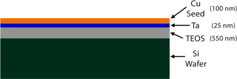
A cross-sectional illustration of the substrate before copper electroplating.
Nine deposition conditions were investigated in this study to evaluate the process parameter windows of interest (Table I). The initial deposition conditions of 80 mA/cm2 peak current density, 0.1 s on-time, and 0.5 s off-time were based off findings from Hsiao et. al., who reported a high degree of nanotwins and texture in electroplated Cu at these conditions [20]. The frequency and duty cycle were varied from this base parameter set. Three samples were deposited per condition, with a target thickness of 3000 ± 300 nm. These thicknesses were evaluated using a Zygo NewView 8300 white light interferometer. For the higher degree of accuracy required for stress measurements, Rutherford Backscattering Diffraction (RBS) and focused ion beam (FIB) cross-sectional thickness measurements were conducted. All three thickness measurement techniques produced similar results and FIB thickness measurements were used for stress approximations.
Table I.
The deposition pulse parameters used in this study.
| PED Condition # | Pulse Signature | |||
|---|---|---|---|---|
| On-Time [ms] | Off-Time [ms] | Frequency [Hz] | Duty Cycle | |
| 1 | 50 | 950 | 1 | 0.05 |
| 2 | 100 | 900 | 1 | 0.1 |
| 3 | 250 | 750 | 1 | 0.25 |
| 4 | 1 | 19 | 50 | 0.05 |
| 5 | 2 | 18 | 50 | 0.1 |
| 6 | 5 | 15 | 50 | 0.25 |
| 7 | 0.5 | 9.5 | 100 | 0.05 |
| 8 | 1 | 9 | 100 | 0.1 |
| 9 | 2.5 | 7.5 | 100 | 0.25 |
2.2 Microstructural Evaluation: EBSD and XRD
The cross-sectional microstructure of the films were evaluated via electron backscattering diffraction (EBSD) on the Hitachi SU-6600 scanning electron microscope (SEM) at Clemson University’s Electron Microscopy Laboratory (United States). To obtain the surface quality necessary for electron backscattering diffraction (EBSD), a sample preparation procedure was used from previous studies [29]. The sample’s cross sections were first polished with diamond lapping paper and finished with a 0.05 μm alumina slurry, followed by FIB milling using the Hitachi NB5000 dual beam SEM/FIB. Inverse pole figures and maps from the EBSD were examined to measure grain sizes, orientations, and twin characteristics of the film cross-sections.
X-ray diffraction (XRD) was performed on the films with the PANalytical XPert3 MRD XRD at the University of Central Florida’s Materials Characterization Facility to confirm the texture results provided by EBSD. The XRD used a 1.5406 Å Cu K-alpha source to measured from 35° to 95° 2θ with a step size of 0.01 and 0.5 s per step. The texture coefficients (TC) of the four major Cu peaks, (111), (200), (220), and (311), were calculated from the diffraction pattern using the following equation:
| (Eq. 1) |
, where is the intensity of the hkl peak of interest, is the peak intensity of randomly oriented Cu, and n is the number of peaks in the diffraction pattern. Figure 2 shows a typical XRD diffraction pattern for a Cu film used in this study.
Figure 2.
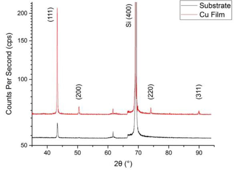
XRD gonio scan pattern of the substrate (bottom) and Cu films (top). The (111), (200), (220), and (311) Cu peaks and the Si (400) substrate peak are labelled.
2.3 Residual Stress Measurements
Biaxial stress ( ) was approximated through the Stoney formula [30] by measuring the radius of curvature of the substrate before and after deposition. The Stoney formula assumes the thickness of the substrate is much larger than that of the film and measures the added stress from its equilibrium state (before deposition). The radius of curvature was obtained through surface mapping with the Zygo NewView 8300 white light interferometer. A 725 um Si wafer thickness and Si (100) material properties [‘thin dielectric films stress extraction’] were used to approximate the biaxial stress in the Cu films.
3. Results and Discussion
3.1 Microstructural Morphology of the Blanket Cu Films
From EBSD results, the cross-sectional grain size of the Cu films for all nine conditions in Table I were determined. Figure 3 shows the grain size distribution of the Cu film cross-section deposited using the PED #5 conditions. The histogram of PED #5 is representative of all the processing conditions examined and reveals a large distribution of grain sizes throughout the films’ cross-sections. A majority of the grains have a diameter between 200 and 300 nm; however, the small and large grains contributed similarly to the overall % grain area. Most small grains were located at the substrate/film interface, while the large grains were mostly present at the film surface. Since the Cu seed layer is only 100 nm thick, it is expected for the grain size to be on the same order of magnitude or smaller than its thickness [31]. As the adatoms build onto one another during deposition, the grains become increasingly larger, as they are no longer restricted by the thickness of the Cu layer. Figure 4 shows that Cu grains larger than 2 μm appear to contribute more to the cross-sectional area of the Cu films in smaller duty cycle deposited films as well as higher pulse frequencies. The shorter on-times and larger off-times allow more recrystallization to occur and reduces the nuclei formation that occurs during the on-time. Prior efforts employing higher current densities resulted in smaller grain sizes in the surface of films [12,14], similar to the findings observed here.
Figure 3.
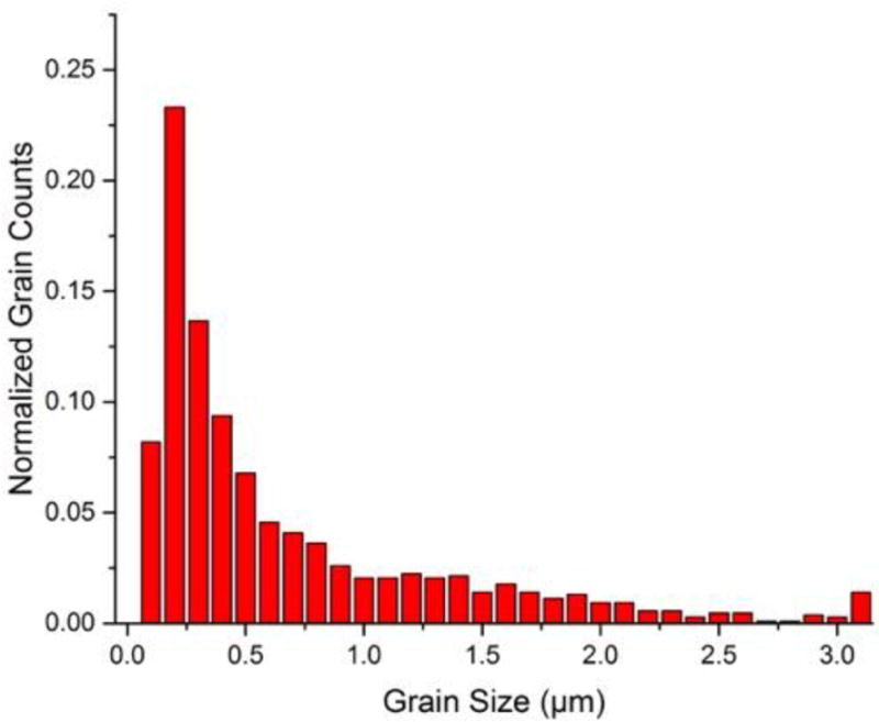
Normalized histogram of the cross-sectional grain sizes found in the Cu films deposited with 0.1 duty cycle and 50 Hz (PED #5) pulse parameters. All deposition pulse parameters produced grain size histograms similar to PED #5.
Figure 4.
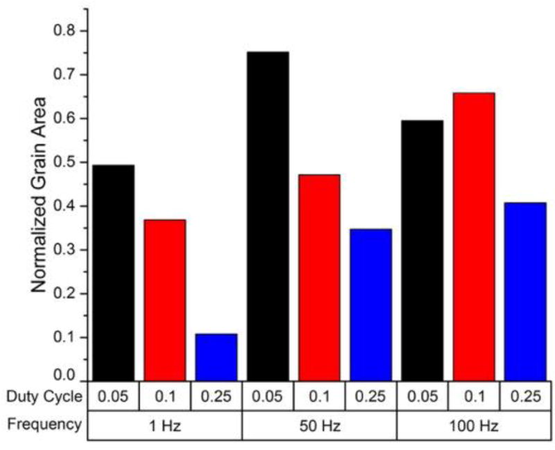
Normalized grain area of grains larger than 2 μm for all nine pulse frequency and duty cycle combinations studied. These “large” grains occupy more area in higher frequency and lower duty cycle depositions.
The roughness also gives insight into the surface morphology of the films. Films with smaller surface grains are expected to have smoother surfaces as is demonstrated in these Cu films illustrated in Figure 5. The increase in roughness with higher frequency depositions correlates with the larger surface grains shown in Figure 4. Surface roughness/grooves can also pin these grains and prevents further grain growth in the case of surface energy minimization driven growth [32–34]. The jump in roughness for the 0.25 duty cycle deposited Cu can be attributed to the significant increase in deposition rate compared to the 0.05 and 0.1 duty cycle deposited films.
Figure 5.
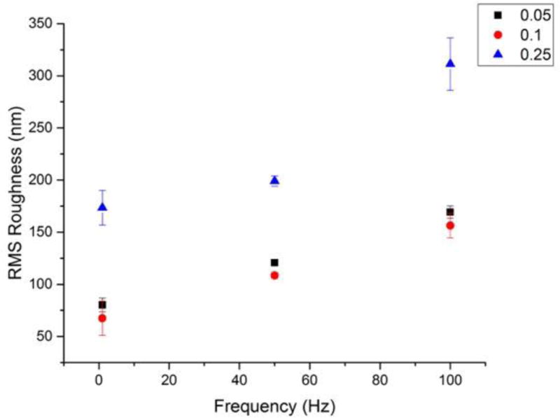
A graph showing the increase in RMS roughness with frequency of the electroplating pulse.
3.2 Texture of the Films
All Cu films exhibited a high degree of (111) preferential orientation normal to the film surface, as verified by both the EBSD and XRD results. Most of these (111)-oriented grains are located near the films’ interface with the substrate as shown in Figure 6b. This is thought to be the result of the preferential (111) orientation of the Cu seed layer. The Cu seed layer was evaluated prior to deposition using an XRD chi rocking curve (shown in Figure 7). The rocking curve measures the intensity of the peak of interest at various chi angles (rotation about the incident beam axis). The rocking curve was conducted at the 2θ position (43.2383°) of the (111) Cu seed peak. The maximum in the chi rocking curve perpendicular to the sample surface (Figure 7) shows the large presence of (111)-oriented grains in the Cu seed layer. Other Cu peaks, (200), (220), and (311), were minimal or indistinguishable in the XRD measurement of the seed layer. As seen in prior studies, the substrate can have a large impact on the orientation of Cu films [22]. While the surface of the films were preferentially oriented, the texture of the in-plane direction for the films were random. The multiple of uniform density (MUD) from the EBSD pole figures and the XRD texture coefficients in Figures 8 and 9 respectively, show similar trends in the (111) texture of the films with changes in pulse on-time. The degree of (111) texture quickly rises with increasing on-times below 5 ms and reaches a maximum at about 50 ms before slowly decreasing at longer on-times. On the other hand, the XRD study (Figure 9) reveals the increased presence of (200) and (311) oriented grains.
Figure 6.
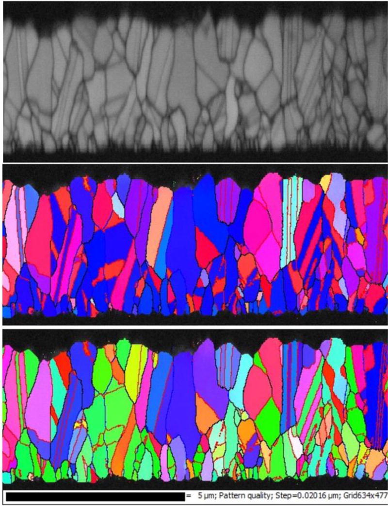
EBSD maps including the band contrast (a), inverse pole figure in the out of plane direction (b), and inverse pole figure of in-plane direction (c) for the copper film cross-sections.
Figure 7.
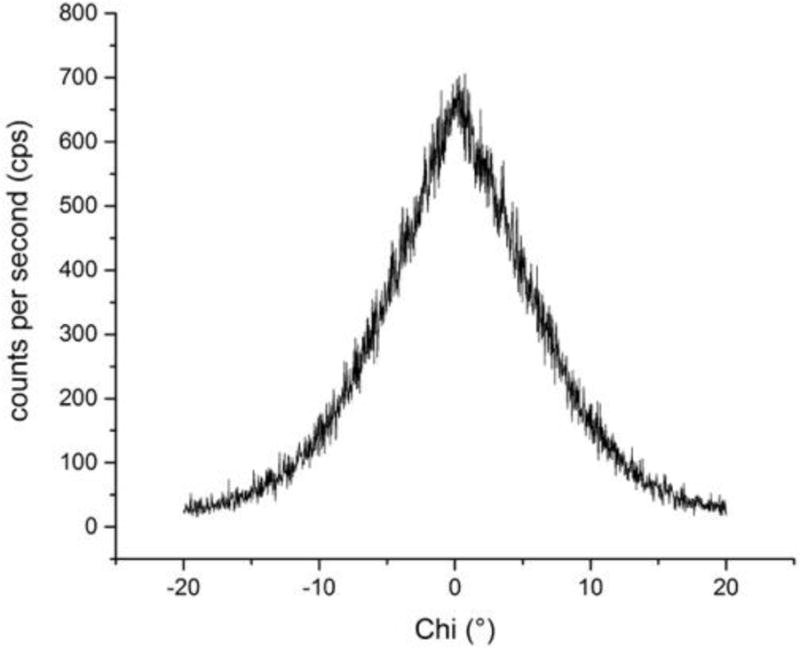
A XRD chi rocking curve of the Cu seed layer prior to deposition, positioned at 43.2383° 2θ for the (111) peak. The maximum at 0° chi indicates a preferential orientation in the (111) in the out-of-plane direction for the Cu layer.
Figure 8.
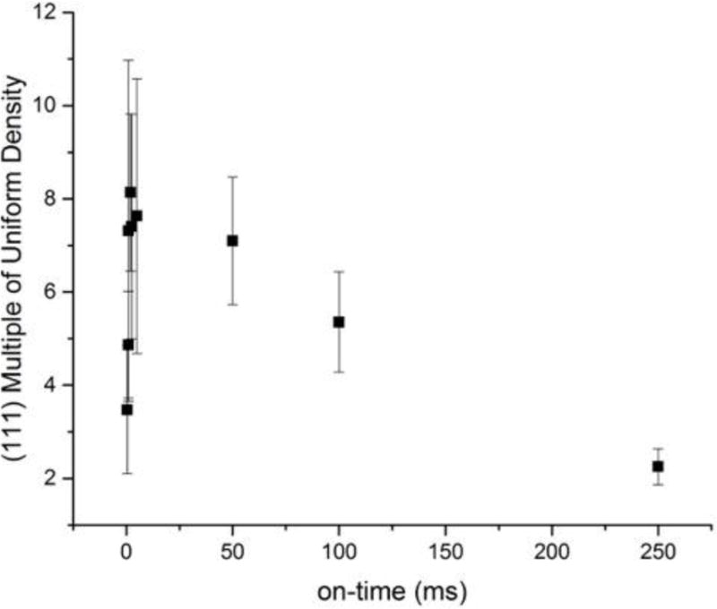
The change in (111) multiple of uniform density number from the EBSD inverse pole figures in the out-of-plane direction with pulse on-time used to deposit the Cu films.
Figure 9.
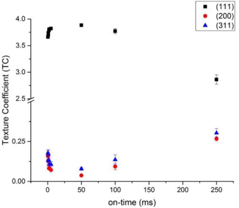
The variation in (111), (200), and (311) XRD texture coefficients calculated from their respective peaks and how they trend with pulse on-time.
Other studies have shown a dependence of the preferential orientation on the pulse current [23]. C. Thompson suggests that (111) textures are driven by surface energy minimization in FCC films, however this only holds true for columnar grains and assumes amorphous substrates, thus does not take into account the substrate texture [35]. He also stated that other orientations, notably (110), are driven by strain energy minimization [35]. While (110) texture in copper films has been derived in many studies [12,16,27], we rarely found any indication of (110)-oriented grains present in this study in the out of plane direction. However, abnormal grain growth of the (100) and (511) orientations are also strain energy driven [36]. As will be shown later, stresses were found to increase with pulse on-times. The elevated stresses enhance strain energy driven grain growth and thus the increase the (200) and (311) presence with on-time.
3.3 Residual Stress in the Films
The biaxial stress was calculated through radius of curvature measurements and the Stoney formula. Higher stresses were found in films that were deposited at lower frequencies (see Figure 10). This follows the findings of D. Xu et. al. [17], that indicated stresses build up during the on-time and anneal out during the off-time of the deposition pulse(s). It is believed, however, that the onset of stress tends to be more rapid than the dissipation of these stresses, leading to the buildup of residual stresses [17]. Figure 11 shows this increase in residual stress with increasing on-time, which occurs due to the rapid nucleation during the on-time. At long on-times (>100 ms), saturation of the nuclei on the surface results in levelling off of the residual stresses in the films. Stress also builds up due to the mismatch in coefficient of thermal expansion between the copper film and the substrate. During cooling, the copper contracts more than silicon wafer causing tensile stresses in the copper. The annealing done during this study was conducted at a low temperature (150 °C) to stabilize the microstructure, which can undergo self-annealing at room temperature [37], without having a major impact on stresses in the copper films. Twinning is one of the mechanisms for stress relief in a material. The number of twins per grain were evaluated from the EBSD band contrast maps and boundary maps of the Cu film cross-sections. A minimum of 0.35 twins/grain were found for all pulsed electroplated film depositions. Furthermore, lower biaxial stresses were found in films with higher twin densities (see Figure 12), which suggests a higher degree of recrystallization in these films. It has been theorized that the formation of nanotwins in Cu films occurs with recrystallization during the pulse off-times [17,19]. No trends were seen in the relationship between the Cu twin density and pulse off-time. Higher off-times actually produced the lowest twin densities in this study. This suggests that the twin density may not be as dependent on pulse off-times as previously thought. However, the twin density increases with increasing grain size [12,38]. As shown in Figure 13, the grain size appears to increase with increasing pulse frequency; films with larger surface grains appear to have more twins. The larger twin density found in the copper films with lower stress may be a manifestation of the thermal stability and mechanical strength of twins [24,26,39,40]. Furthermore, atomic rearrangement occurred more frequently in 50 Hz and 100 Hz deposited films, during breaks in the on-time, allowing more twins to form in these films.
Figure 10.
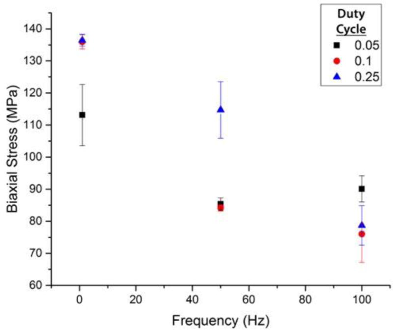
A graph showing a decrease in biaxial stress for the Cu films with increases in pulse frequency during deposition.
Figure 11.
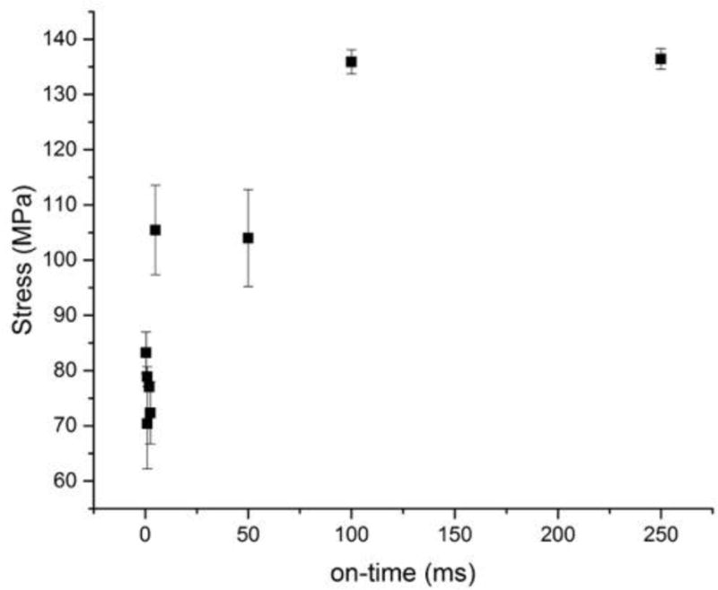
A graph showing larger biaxial stresses in Cu films that were deposited with longer pulse on-times.
Figure 12.
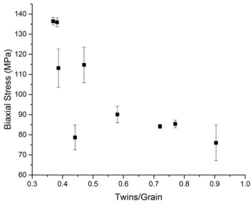
The correlation between twins per grain and biaxial stress in the Cu films.
Figure 13.
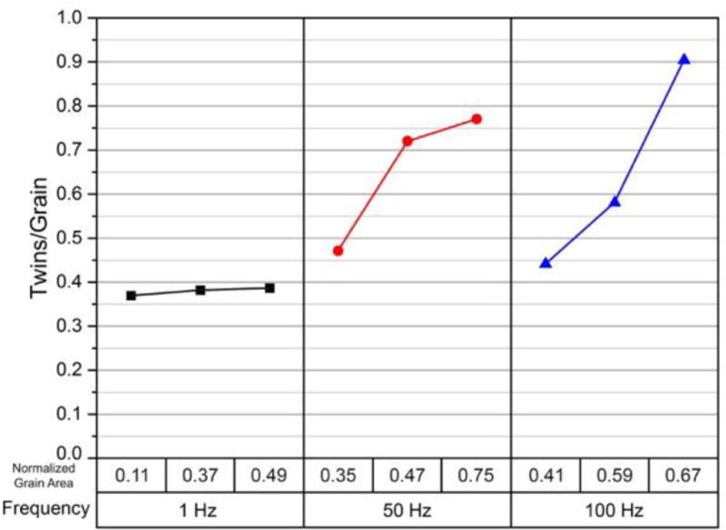
The dependence of twinning on the area of large grains (>2 μm) in the Cu films, separated by pulse frequency used during deposition.
Conclusion
The influence of pulsed electroplating frequency and duty cycle were evaluated for Cu film stress state and microstructural characteristics, including grain morphology, grain orientations, and twinning. The cross-sectional surface grain size decreased with lower frequencies and higher duty cycles due to increased nucleation rates of the Cu. The films had varying degrees of (111) preferential orientation in the out of plane direction. The decrease in (111)-oriented grains with longer pulse on-times was attributed to the increased biaxial stresses in the Cu films, resulting in strain energy minimization driven growth of the (100) and (311) oriented grains. The biaxial stresses in the Cu films were also lower for films deposited with lower on-times and films that contained higher twin densities. The twins act as stress relieving mechanisms, but also stabilize the microstructure and increase strength of the Cu films. This is further evidence that high densities of twins in Cu microstructures will increase the reliability of microelectronic interconnects.
Acknowledgments
The authors would like to thank the National Institute of Standards and Technology (NIST) for financial support of this project under grant no. 60NANB12H016N. The access and support of the Materials Characterization Facility (MCF) and their staff at the University of Central Florida is also greatly appreciated.
Footnotes
Certain commercial equipment, instruments, or materials are identified in this paper to specify experimental or theoretical procedures. Such identification does not imply recommendation by NIST nor the authors, nor does it imply that the equipment or materials are necessarily the best available for the intended purpose.
References
- 1.Pratt A. Overview of the Use of Copper Interconnects in the Semiconductor Industry. Adv Energy Ind. 2004 [Google Scholar]
- 2.Radisic A, Lühn O, Philipsen HG, El-Mekki Z, Honore M, Rodet S, Armini S, Drijbooms C, Bender H, Ruythooren W. Copper plating for 3D interconnects. Microelectronic Engineering. 2011;88:701–704. [Google Scholar]
- 3.Holmbom G, Jacobsson B. Through-hole plating of Cu by modulated current deposition. Surface and Coatings Technology. 1988;35:333–341. [Google Scholar]
- 4.Ryu C, Kwon K, Loke AL, Lee H, Nogami T, Dubin VM, Kavari RA, Ray GW, Wong SS. Microstructure and reliability of copper interconnects. Electron Devices, IEEE Transactions on. 1999;46:1113–1120. [Google Scholar]
- 5.Lu L, Shen Y, Chen X, Qian L, Lu K. Ultrahigh strength and high electrical conductivity in copper. Science. 2004;304:422–426. doi: 10.1126/science.1092905. [DOI] [PubMed] [Google Scholar]
- 6.Chen K, Wu W, Liao C, Chen L, Tu KN. Observation of Atomic Diffusion at Twin-Modified Grain Boundaries in Copper. Science. 2008;321:1066–1069. doi: 10.1126/science.1160777. [DOI] [PubMed] [Google Scholar]
- 7.Wang J, Zhang X. Twinning effects on strength and plasticity of metallic materials. MRS Bull. 2016;41:274–281. [Google Scholar]
- 8.Chandrasekar MS, Pushpavanam M. Pulse and pulse reverse plating—Conceptual, advantages and applications. Electrochim Acta. 2008;53:3313–3322. [Google Scholar]
- 9.Takahashi KM. Electroplating Copper onto Resistive Barrier Films. Journal of The Electrochemical Society. 2000;147:1414–1417. [Google Scholar]
- 10.Ponnuswamy T, Sukamto J, Reid J, Mayer S. Two step copper electroplating process with anneal for uniform across wafer deposition and void free filling on ruthenium coated wafers. 7,964,506. US Patent No. 2011
- 11.Akram S, Watkins CM, Hiatt WM, Hembree DR, Wark JM, Farnworth WM, Tuttle M, Rigg S, Oliver S, Kirby K, Wood A, Velicky L. Through-wafer interconnects for photoimager and memory wafers. 7,300,857. US Patent No. 2010
- 12.Lui G, Chen D, Kuo J. EBSD characterization of twinned copper using pulsed electrodeposition. J Phys D. 2009;42:215410. [Google Scholar]
- 13.Zeng L, Xu S, Tan J, Zhang L, Zhang W, Wang L, Qu X. Copper pulse plating on Ru/TaSiN barrier. Solid-State and Integrated Circuit Technology. 2006:345–347. [Google Scholar]
- 14.Natter H, Hempelmann R. Nanocrystalline Copper by Pulsed Electrodeposition: The Effects of Organic Additives, Bath Temperature, and pH. J Phys Chem. 1996;100:19525–19532. [Google Scholar]
- 15.Tzeng G, Wan C. The anion effect of the morphology and preferred orientation of copper deposit under pulse current conditions. Mater Chem Phys. 1991;27:77–107. [Google Scholar]
- 16.Lin YW, Kuo JC, Lui KT, Chen D. Effect of plating current density and frequency on the crystallographic texture of electrodeposited copper. Materials Science Forum. 2010;638:2841–2845. [Google Scholar]
- 17.Xu D, Sriram V, Ozolins V, Yang J, Tu K, Stafford GR, Beauchamp C. In situ measurements of stress evolution for nanotwin formation during pulse electrodeposition of copper. J Appl Phys. 2009;105:023521. [Google Scholar]
- 18.Xu D, Sriram V, Ozolins V, Yang J, Tu KN, Stafford GR, Beauchamp C, Zienert I, Geisler H, Hofmann P, Zschech E. Nanotwin formation and its physical properties and effect on reliability of copper interconnects. Microelectronic Engineering. 2008;85:2155–2158. [Google Scholar]
- 19.Xu D, Kwan WL, Chen K, Zhang X, Ozoliņš V, Tu K. Nanotwin formation in copper thin films by stress/strain relaxation in pulse electrodeposition. Appl Phys Lett. 2007;91:254105. [Google Scholar]
- 20.Hsiao H, Liu C, Lin H, Liu T, Lu C, Huang Y, Chen C, Tu K. Unidirectional Growth of Microbumps on (111)-Oriented and Nanotwinned Copper. Science. 2012;336:1007–1010. doi: 10.1126/science.1216511. [DOI] [PubMed] [Google Scholar]
- 21.Lee H, Ning W, Zhu C, Xu G, Luo L, Tian S. Fabrication and microstructure evolution of preferred oriented nanotwinned copper by pulse electroplating for RDL in WLP. Electronic Packaging Technology (ICEPT) 2013:292–295. [Google Scholar]
- 22.Cui BZ, Han K, Xin Y, Waryoba DR, Mbaruku AL. Highly textured and twinned Cu films fabricated by pulsed electrodeposition. Acta Materialia. 2007;55:4429–4438. [Google Scholar]
- 23.Zhang X, Tu K, Chen Z, Tan Y, Wong CC, Mhaisalkar SG, Li X, Tung C, Cheng C. Pulse electroplating of copper film: a study of process and microstructure. Journal of nanoscience and nanotechnology. 2008;8:2568–2574. [PubMed] [Google Scholar]
- 24.Lu L, Chen X, Huang X, Lu K. Revealing the Maximum Strength in Nanotwinned Copper. Science. 2009;323:607–610. doi: 10.1126/science.1167641. [DOI] [PubMed] [Google Scholar]
- 25.Xiang Y, Tsui TY, Vlassak JJ. The mechanical properties of freestanding electroplated Cu thin films. J Mater Res. 2006;21:1607–1618. [Google Scholar]
- 26.Zhao Y, Furnish TA, Kassner ME, Hodge AM. Thermal stability of highly nanotwinned copper: The role of grain boundaries and texture. J Mater Res. 2012;27:3049–3057. [Google Scholar]
- 27.Hong B, Jiang C, Wang X. Influence of complexing agents on texture formation of electrodeposited copper. Surface and Coatings Technology. 2007;201:7449–7452. [Google Scholar]
- 28.Kohama K, Ito K, Matsumoto T, Shirai Y, Murakami M. Role of Cu film texture in grain growth correlated with twin boundary formation. Acta Materialia. 2012;60:588–595. [Google Scholar]
- 29.Marro J, Okoro C, Obeng Y, Richardson K. Defect and microstructural evolution in thermally cycled Cu through-silicon vias. Microelectronics Reliability. 2014;54:2586–2593. [Google Scholar]
- 30.Stoney GG. The tension of metallic films deposited by electrolysis. Proceedings of the Royal Society of London. Series A, Containing Papers of a Mathematical and Physical Character. 1909;82:172–175. [Google Scholar]
- 31.Thompson C. Grain-Growth in Thin-Films. Annu Rev Mater Sci. 1990;20:245–268. [Google Scholar]
- 32.Mullins WW. The effect of thermal grooving on grain boundary motion. Acta Metallurgica. 1958;6:414–427. [Google Scholar]
- 33.Frost HJ. Microstructural evolution in thin films. Mater Charact. 1994;32:257–273. [Google Scholar]
- 34.Barmak K, Eggeling E, Kinderlehrer D, Sharp R, Ta’asan S, Rollett AD, Coffey KR. Grain growth and the puzzle of its stagnation in thin films: The curious tale of a tail and an ear. Progress in Materials Science. 2013;58:987–1055. [Google Scholar]
- 35.Thompson CV. Texture evolution during grain growth in polycrystalline films. Scripta Metallurgica et Materialia. 1993;28:167–172. [Google Scholar]
- 36.Zielinski EM, Vinci RP, Bravman JC. Effects of barrier layer and annealing on abnormal grain growth in copper thin films. J Appl Phys. 1994;76:4516–4523. [Google Scholar]
- 37.Okoro C, Vanstreels K, Labie R, Lühn O, Vandevelde B, Verlinden B, Vandepitte D. Influence of annealing conditions on the mechanical and microstructural behavior of electroplated Cu-TSV. J Micromech Microengineering. 2010;20 [Google Scholar]
- 38.Yu Q, Shan Z, Li J, Huang X, Xiao L, Sun J, Ma E. Strong crystal size effect on deformation twinning. Nature. 2010;463:335–338. doi: 10.1038/nature08692. [DOI] [PubMed] [Google Scholar]
- 39.Li H, Zhu C, Tian S, Xu G, Luo L. Thermomechanical behavior of nanotwinned copper interconnection line in wafer level packaging and the influence on wafer warpage. Electronic Components and Technology Conference (ECTC) 2015:1228–1233. [Google Scholar]
- 40.Zhang X, Misra A. Superior thermal stability of coherent twin boundaries in nanotwinned metals. Scr Mater. 2012;66:860–865. [Google Scholar]


