Abstract
This paper presents the design and feasibility study of a very-high resolution gamma camera for detecting 27–35 keV X and gamma rays emitted by I-125 labelled radiotracers. This detector consists of a newly developed Electron-multiplying CCD (EMCCD) sensor and a de-magnifier tube coupled to a thin layer of scintillator. A prototype detector was developed and experimentally evaluated. This detector has a detection area of ~ 5 cm2. It provided an intrinsic spatial resolution of < 60 µm FWHM and a high signal-to-noise ratio for detecting the 27–35 keV photons, which ensures an excellent counting efficiency. This detector will be used as the key component for a single photon emission microscope (SPEM) system that is under development.
Index Terms: De-magnifier tube, EMCCD
I. Introduction
PINHOLE and multiple pinhole gamma cameras are widely used for imaging the distribution of radio-labeled molecules in small lab animals [1]–[5]. One of the advantages of SPECT imaging is that it is possible to achieve a spatial resolution superior to that provided by Positron Emission Tomography (PET). Detectors with 1–2 mm intrinsic resolution have been used to achieve an excellent spatial resolution in reconstructed SPECT images [6]–[10]. However, these systems in general used apertures having a relatively small number of micro pinholes. This leads to a very low detection efficiency and limits their use for quantitative studies. One possible approach for improving the tradeoff between detection efficiency and spatial resolution is to start from very high resolution gamma ray sensors and use them with apertures having a large number of micro pinholes. The aperture can be placed very close to the detector to reduce data multiplexing [11], [12]. Over the past several years, advances in detector technology have pushed the intrinsic spatial resolution of gamma ray detectors down to a few hundred microns or even better. Several groups have proposed SPECT imaging systems based on these newly developed sensors [13]–[17].
We are developing a single photon emission microscope (SPEM) system for small animal imaging based on I-125 labeled radiotracers [18], [19]. It uses an ultra-high resolution gamma ray detector with a converging and non-multiplexing collimator. By confining the field-of-view to a small sub-region inside the object, we can pack a large number of micro-pinholes without any overlapping in projections through these pinholes. Therefore, a relatively good detection efficiency can be achieved along with an excellent imaging resolution. In this paper, we report the design and preliminary performances of the key component for the SPEM system, an ultra-high resolution gamma camera. This detector is based on a newly developed EMCCD sensor and a de-magnifier tube, coupled to a thin layer of scintillator. The prototype detector has an active area of ~5 × 5 cm2. An intrinsic spatial resolution of < 60 µm and an excellent signal-to-noise ratio for detecting low energy gamma rays have been experimentally demonstrated.
II. Materials and Methods
A. Requirements on Detectors for the SPEM System
Radioisotope I-125 decays via electron capture with the emission of a 35 keV gamma ray. Several K shell X-rays with photon energies ranging from 27 to 32 keV from the 125 Te daughter product can accompany the decay. The relative probabilities for photon emissions associated with I-125 decay are 53% at 27.2 keV, 100% at 27.5 keV, 28.6% at ~31 keV and 9% at 35 keV. I-125 labeled probes have found many applications in molecular biology research [20]–[22]. Due to the relatively low photon energies, it is possible to collimate and locate these photons with very high precision. The performance goal of the SPEM system is to deliver a spatial resolution of a few hundred microns in mice using I-125 labeled radiotracers. Several design considerations for the detector used are summarized as the following. First, the detector should have an excellent intrinsic spatial resolution. The design of this camera should allow an intrinsic detector spatial resolution of < 50 µm FWHM to be achieved. Secondly, for 27–35 keV photons, most of the interactions are photoelectric and the energy loss due to Compton scattering is relatively small. In this energy range, scattering rejection based on energy information is both less feasible and less important compared to SPECT imaging at higher gamma ray energies. The emphasis for this detector is to ensure a very high efficiency for detecting (or counting) true X and gamma ray interactions without counting dark events. Thirdly, in the design of the SPEM system, we used apertures with micro-pinholes of 100 µm diameter to ensure a very high imaging resolution. This leads to a relatively low photon flux reaching the detector. We expect that the maximum count rate per detector is a few thousand counts per second. For constructing a practical imaging system, the detector was designed to have an active area of greater than 5 × 5 cm2.
B. A Very-High Resolution Gamma Ray Detector
The detector that we developed for this application is essentially a single X/gamma ray photon counting camera. It is based on the newly developed electron multiplying charge-coupled devices (EMCCD). These sensors are similar, in structure, to conventional CCDs except that a series of multiplying registers are added before the readout amplifier. These multiplying registers amplify the charge signal by a factor of up to several tens of thousand using the phenomenon called “impact ionization” [23], [24]. This effectively eliminates the readout electronic noise associated with conventional CCDs (especially with fast-scan CCDs). As a result, EMCCDs can offer a readout rate of up to 35 MHz, while having an effective readout noise of < 1 electron RMS per pixel. As a comparison, standard CCDs at similar readout rates would have a readout noise of 40 electrons or more.
The combination of high spatial resolution, high frame rate and low effective readout noise has made the EMCCD a promising device for gamma ray imaging applications. Several groups have proposed or experimentally tested imaging systems based on this device. Unfortunately, currently available sensors are relatively small (typically 8 × 8 mm2 in size). To construct a detector with a reasonable active area, Nagarkar, et al. [25] have developed a detector system that used an optical lens to couple a scintillation array to an EMCCD device. The major limitation of this design is the low coupling efficiency between the scintillator and the EMCCD sensor, which was measured to be 0.7–0.07%. For our applications (of imaging at ~30 keV), each gamma ray stopped in the phosphor produces only a few hundred photons. After coupling to the EMCCD sensor, the remaining photons may also be shared between several CCD pixels, which further reduces the signal-to-noise ratio per pixel. The coupling efficiency can be improved by using fiber tapers [15], [16]. For example, a 4:1 taper coupled to the sensor would bring the active area up to 32 × 32 mm2 and provide an effective light transmission of < 5%. However, this coupling efficiency is still too low for reliably detecting single X/gamma ray interactions (at ~ 30 keV). Furthermore, using tapers with aspect ratios greater than 3:1 would also introduce considerable optical distortions.
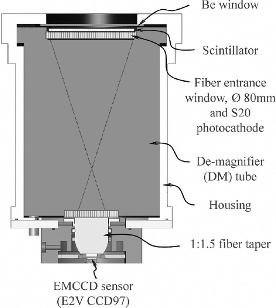
In our detector design, we used an electrostatic de-magnifier (DM) tube, instead of fiber tapers or relay lenses, for coupling scintillation light onto the EMCCD sensor. The DM tube is essentially a first generation image intensifier which has a quantum efficiency (QE) of ~7% at around 550 nm wavelength [26]. It has an active area of ~80 mm diameter on the front entrance window, which is surrounded by a dead area of ~1.5 cm wide for accommodating the tube structure. The entire active area is covered by a thin layer of phosphor. Unlike using a fiber taper, the use of the DM tube provides an enlarged active area with a fixed photon gain. So it is preferred when a large de-magnification ratio (DM ratio) is required between the actual detection area and the active area of the readout sensor used. However, the spatial resolution at the input window of the DM tube is inversely proportional to the DM ratio. A large DM ratio will also lead to significant distortions at the edge of the FOV. In our detector, we chose to use a moderate DM ratio of 4:1. The output of the DM tube is coupled to the EMCCD sensor through a 1.5:1 fiber taper. Therefore, the total detection active area on the phosphor is ~50 × 50 mm2. We can further extend the active area to cover up to 80 mm diameter, by using a larger DM ratio. This will leave a minimum dead area of ~1.5 cm wide around the detection area. A schematic of the gamma camera is shown in Fig. 1. In our prototype device, a Gadox phosphor of ~80 µm thickness is used for converting the 27–35 keV X/Gamma rays into visible photons. Several other scintillation materials, such as columnar CsI(Tl), will be tested in future studies. The EMCCD sensor used is an E2V 97 series L3 Vision Electron Multiplication CCD [27]. It has 512 × 512 pixels and each pixel is 16 × 16 µm2 in size. This sensor is a back-illuminated frame transfer device. It operates at up to 10 MHz so that an effective frame rate of 32 frames per second (fps) can be achieved at full resolution. The sensor is normally operating at −40°C to reduce dark current.
Fig. 1.
The prototype ultra-high resolution gamma camera based on an EMCCD sensor and a DM tube.
To extract gamma ray interactions from a frame acquired, we first find local maxima in the frame. An array of 3 × 3 to 5 × 5 pixels (depending on the binning scheme used) was then defined around each peak position. The energy of an interaction is derived by summing signals from all pixels in the corresponding group, while the interaction position is estimated by simply centroiding over the same group of pixels.
III. Results and Discussions
A. Signal-to-Noise Ratio and Energy Resolution
For each 27–35 keV photon energy deposited in the phosphor, ~600 scintillation photons are generated (the light yield of the Gadox phosphor was assumed to be ~22 400 photon/MeV [28]). Considering that only a relatively small portion of these photons can exit from the phosphor and the quantum efficiency (Q.E.) of the photocathode is as low as 5–7%, we expect ~10 photoelectrons to be emitted from the photocathode. The DM tube used has a gain of ~60 photons/photoelectron, which leads to around 600 photons emitted from its output window per event. After taking into account the transmission of the fiber taper and the quantum efficiency of the EMCCD sensor, the number of electrons generated on the EMCCD is a Poisson random variable with a mean of ~100 electrons. These electrons are typically spread over 4 × 4 or 5 × 5 pixels. Such a signal is rather weak for a standard CCD readout at 10 MHz, but it is more than plenty for the EMCCD sensor to handle. We have defined a conversion efficiency λ, which is the mean number of electrons generated on the EMCCD sensor for a single photoelectron on the DM photocathode. For the prototype detector, λ is ~10. Different conversion efficiency λ can be achieved by using tapers of different sizes between the DM tube and the EMCCD sensor.
The internal gain of EMCCD sensors is a stochastic process. For a fixed number (n) of electrons at the input of the multiplication stage, the number of electrons at the output (m) follows the distribution given in [29],
| (1) |
where G is the electron multiplying (EM) gain. With the input signal Sin being a Poisson random variable, the output signal Sout has a mean
| (2) |
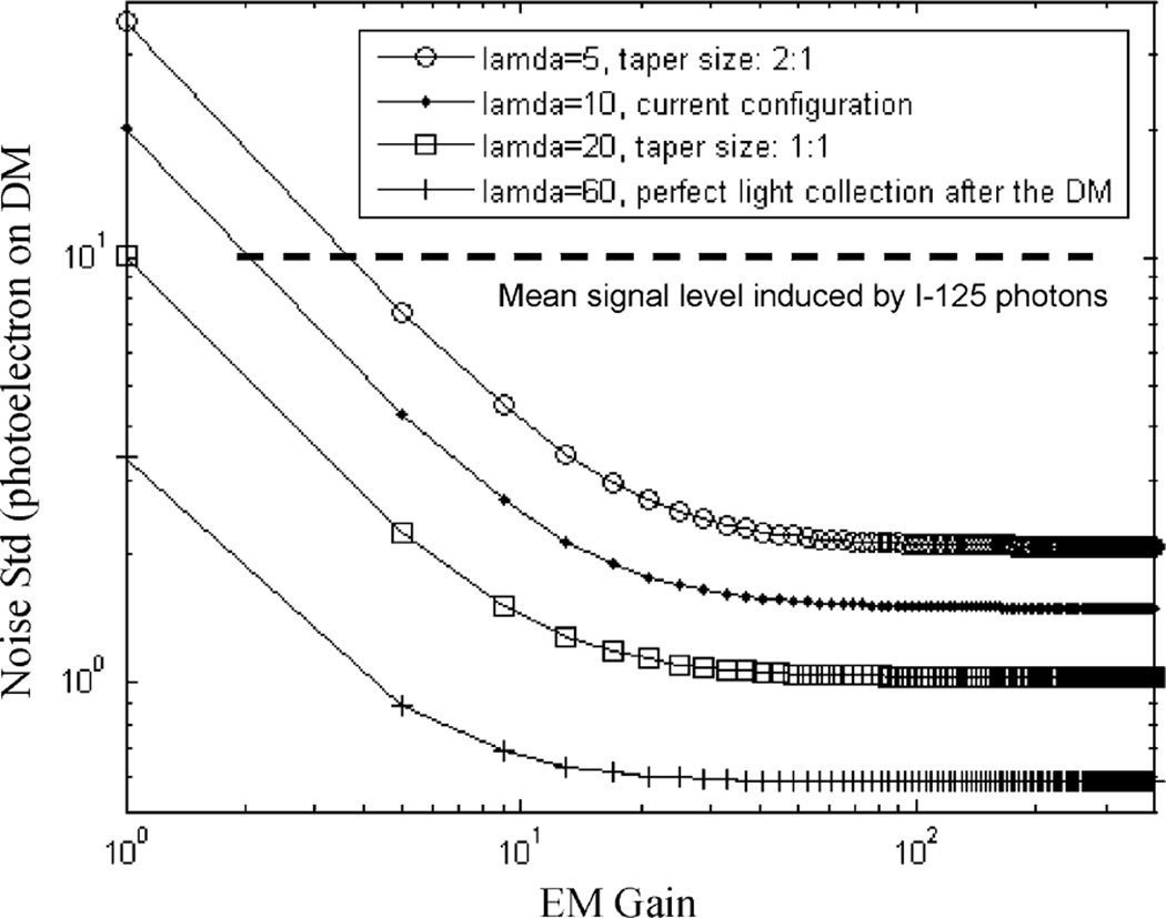
and standard deviation where N is the number of multiplying registers in the EMCCD, which is 550 in the sensor used in our detector. Now considering the spurious noise charge generated during the transfer of charge through the device (i.e., the clock-induced charge, CIC) and thermal dark noise as in standard CCDs, the overall readout noise for a given signal Ne is [29] where npix is the number of pixels included when deriving the overall signal level by summing over a local group of pixels. Nspurious and Ndark are the average noise charge per pixel within a given exposure time, typically 10–30 ms. σreadout is the readout noise of the EMCCD output amplifier. Note that CIC is a common phenomenon for all CCD sensors. It is normally lost in the CCD readout noise in even the lowest noise conventional CCDs. However for the EMCCD at high gain, even individual electrons can be seen as sharp spikes in the image and any CIC will become visible. To keep clock induced charge to a minimum, careful attention has to be paid to the clock amplitudes and edges [29]. In (4), σtotal is given in the number of electrons on the input of the CCD before multiplication. Estimated total readout noise for a given fixed signal of 10 photoelectrons, as a function on the EM gain, are shown in Fig. 2. For these calculations, we assumed that npix = 25 and σreadout = 40e−/pix. Nspurious and Ndark are both negligible when compared to typical amplitudes of true signals. With an EM gain of a few hundred, the total readout noise for the given signal level (~10 photoelectrons) was around 1 photoelectrons. Clearly, the energy resolution achievable with this detector is dominated by the Poisson fluctuation on the number of photoelectrons generated on the DM photocathode (σ > 4 photoelectrons) rather than the subsequent readout noise.
Fig. 2.
Overall readout out noise for a given signal of 10 photoelectrons on the DM photocathode. l’s are the conversion efficiency from photoelectrons (on DM) to electrons on CCD.
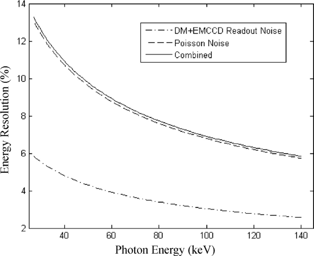
Although the emphasis of this work is to achieve an ultra-high spatial resolution of υ µm, a good energy resolution may also be obtained with detectors having similar configurations. One possible approach is to maximize the photoelectron yield on the DM tube by depositing a photocathode directly on a thin layer of scintillator and using it as the entrance window. D’Ambrosio, et al. [31] have shown that a photoelectron yield of > 4 photoelectron/keV can be achieved with a thin YAP window. In principle, the photoelectron yield can be further improved by the use of new scintillators such as LaBr (Ce) (light-yield: 65000 ph/MeV). Pani et al. [32] have recently reported an energy resolution of 6% at 140 keV in an gamma camera, using a commercially available 2” × 2” LaBr3 (Ce) scintillator coupled to a PSPMT. Even with a perfect scintillator (free of non-linearity and light-yield dependency on interaction location), it would take at least 1500 photons at 140 keV to achieve a resolution of 6%. So we would expect that > 10 photoelectrons/keV was achieved with their setup. If we use a DM tube that has a thin quartz entrance window with a similar photocathode and all other configurations kept the same as in our current prototype detector, we should get a light pool containing > 300 photoelectrons for each 30 keV deposited in the crystal. This should greatly improve the SNR for detecting I-125 interactions. In Fig. 3, we showed the estimated contributions to the overall energy resolution from the Poisson fluctuation on the number of photoelectrons and the subsequent readout noise.
| (3) |
| (4) |
From this data, it should be possible to achieve an energy resolution of ~20% FWHM at ~30 keV and ~60% at 140 keV with the gamma camera based on DM tube and EMCCD readout.
Fig. 3.
Estimated energy resolution with Poisson noise and readout noise only. A photoelectron yield of 10 photoelectrons/keV was assumed for these calculations.
B. X and Gamma Ray Photon Counting Capability
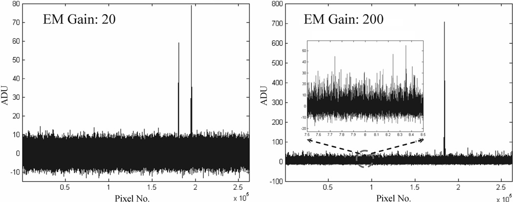
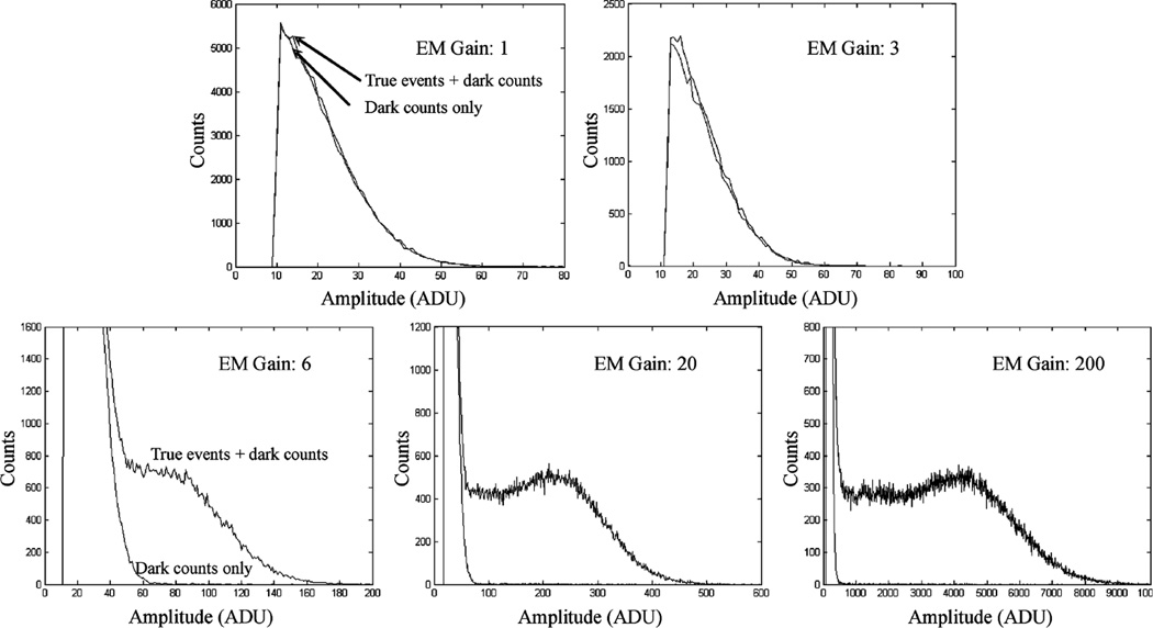
Some examples of detected I-125 interactions are shown in Fig. 4. With a reasonable electron multiplying gain, the resulting signal amplitudes from true interactions are well above the noise. At a gain of 200, we can see some low amplitude spikes on top of the remaining readout noise, for pixels without true signal. These are caused by thermally generated photoelectrons on the DM photocathode, at a rate of ~50 photoelectrons/sec.cm2. For gamma ray photon counting applications, we set a threshold on the summed signal from a local group of 4 × 4 or 5 × 5 pixels. At a frame rate of 30 f/s or higher, the chance of two thermally generated photoelectrons falling onto the same group of pixels and within the same frame is negligible. Therefore one can set a threshold on summed signals that is just above a signal photoelectron level to pick up true I-125 events. As previously discussed, the mean signal level for I-125 events is ~10 photoelectrons, which should be well-separated from the signal level for dark events.
Fig. 4.
Two experimentally derived frames that contain true I-125 interactions. Note that the low amplitude spikes corresponding to thermally generated photoelectrons from the DM photocathode are visible at an EM gain of 200.
To further verify the X and gamma photon-counting capability of this prototype detector, we used a collimated I-125 source to irradiate the detector. One third of its 5 × 5 cm2 active area was exposed to the source, while the rest of the active area was shielded by tungsten sheets of 1 mm thickness. Measured energy spectra with events from both shielded and open areas (normalized to the same size and exposure time) are compared in Fig. 5. Note that there is a severe low-energy tailing effect in measured spectra with true events. This is mostly caused by the variation in light yield (depending on where the gamma ray energy is deposited in the scintillator). In the Gadox phosphor used, absorption material is added to reduce light spread. As a result, scintillation photons generated further away from the exiting surface would suffer more attenuation. We expect that this effect can be reduced using scintillators with a more uniform light yield. With an EM gain of 200, one can set an energy threshold at around 1/8 of the signal amplitude for photopeak events. This should give a > 90% counting efficiency for true events, with almost complete rejection of dark events. This excellent gamma ray photon counting efficiency is critical for the SPEM application because the true count rate may be as low as a few tens of counts per second.
Fig. 5.
Measured energy spectra for true events plus dark counts (blue) and dark counts only (red).
C. Intrinsic Spatial Resolution
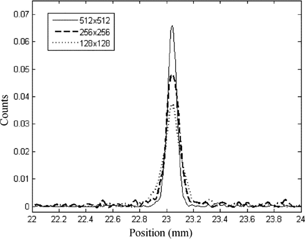
The intrinsic spatial resolution of the prototype detector was measured with an I-125 spherical source of 500 µm diameter, placed 10 cm away from the detector. A slit collimator made of 1 mm thick tungsten sheet was placed right on top of the scintillator. The slit opening on the collimator was ~25 µm wide. For this measurement, we used different binning schemes when reading out the EMCCD sensor. The use of 2 × 2 and 4 × 4 binning improve the readout frame rate from the standard 32 fps to 50 fps and 95 fps, respectively. This helps to reduce the probability of event overlapping at high count rate. However, binning does lead to poorer spatial resolution due to the enlarged optical pixel size on the detector. The measured line response functions are shown in Fig. 6. The measured intrinsic spatial resolution of the detector is shown in Table I. The effect of slit width was subtracted in quadrature from the measured FWHM of LSF.
Fig. 6.
Measured line spread functions with 1 × 1, 2 × 2 and 4 × 4 binning.
TABLE 1.
Measured Detector Intrinsic Spatial Resolution
| EMCCD Binning |
Readout Frame Rate (fps) |
Optical Pixel Size (µm) |
FWHM (µm) |
FWTM (µm) |
| 512×512 | 32 | 96 | 60 | 123 |
| 256×256 | 54 | 192 | 92 | 190 |
| 128×128 | 95 | 384 | 119 | 227 |
Note that when reading out the detector with 512 × 512 pixels, the intrinsic spatial resolution achieved was around 60 µm FWHM, which is slightly worse than the target (< 50µm). In this prototype detector, we used a Gadox phosphor for converting gamma rays into visible photons. This scintillator is wet powder applied on the input window of the DM tube. Its polycrystalline structure leads to a relatively wide light spread. Results in Table I showed that even with 4 × 4 binning and the resultant 384 × 384 µm pixel size, one can still get a good spatial resolution of 119 µm FWHM. This indicated that the light spread in the scintillator must be wide enough to cover at least 2 × 2 pixels or an area of 800 × 800 µm To further improve the spatial resolution, we will test other scintillators that are either brighter or have less light spread, such as columnar CsI(Tl) or a thin disk of YAP or LaBr (Ce). As we previously discussed, it is possible to achieve more than 10 photoelectrons/keV, in contrast to the 0.3–0.5 photoelectrons/keV that we are currently getting. These should help to achieve a better detector intrinsic spatial resolution.
D. Preliminary Pinhole Imaging Studies
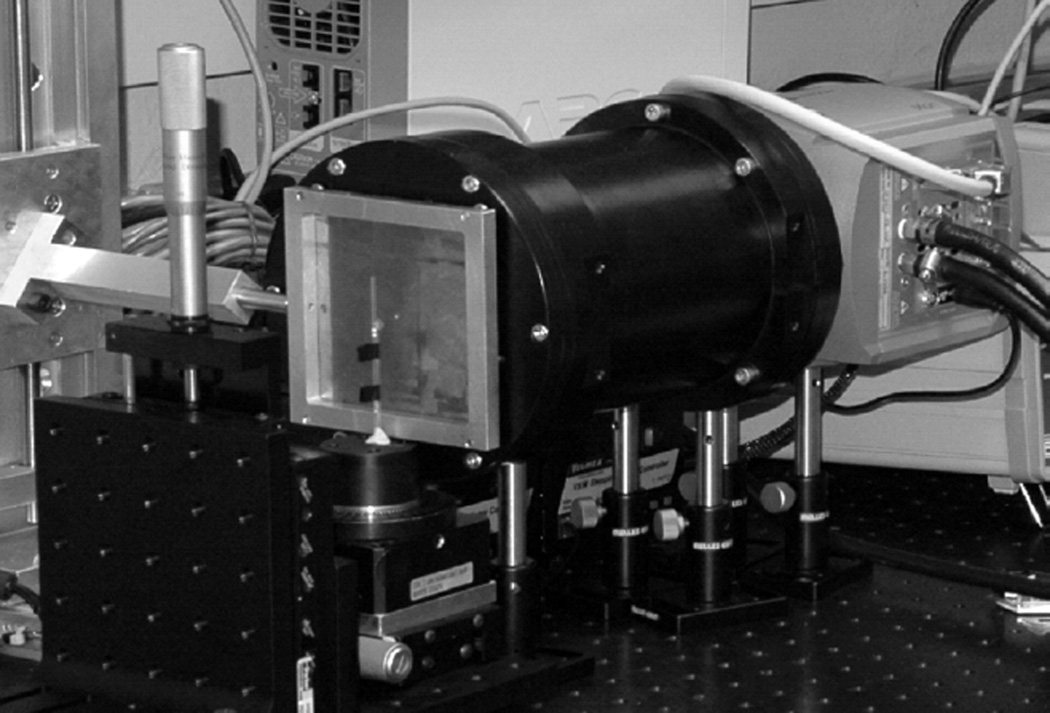
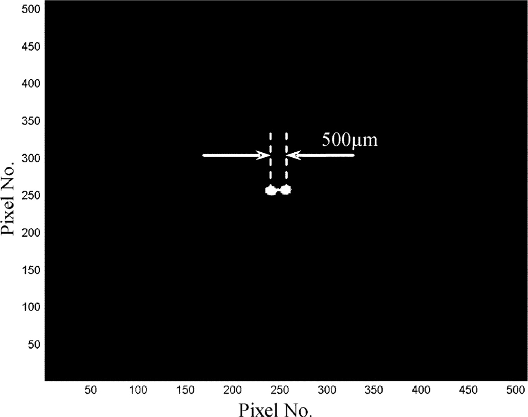
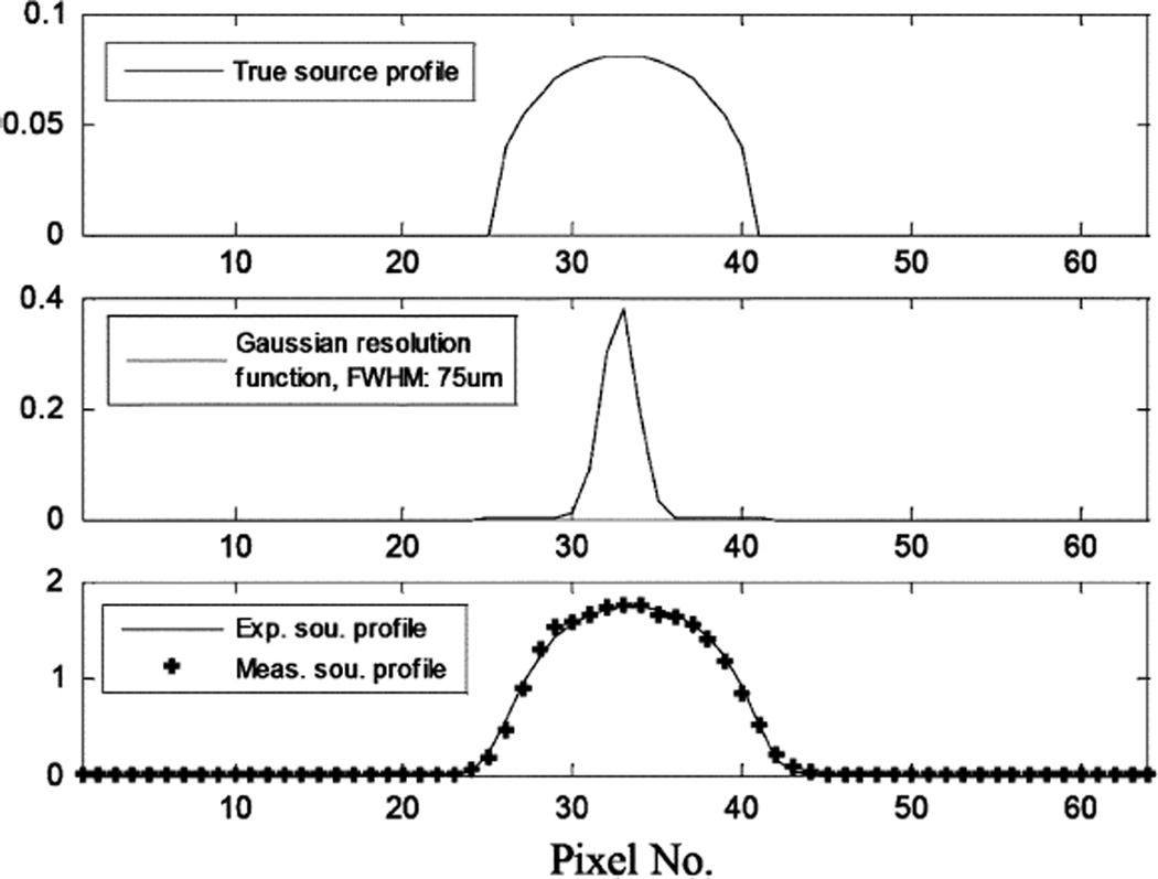
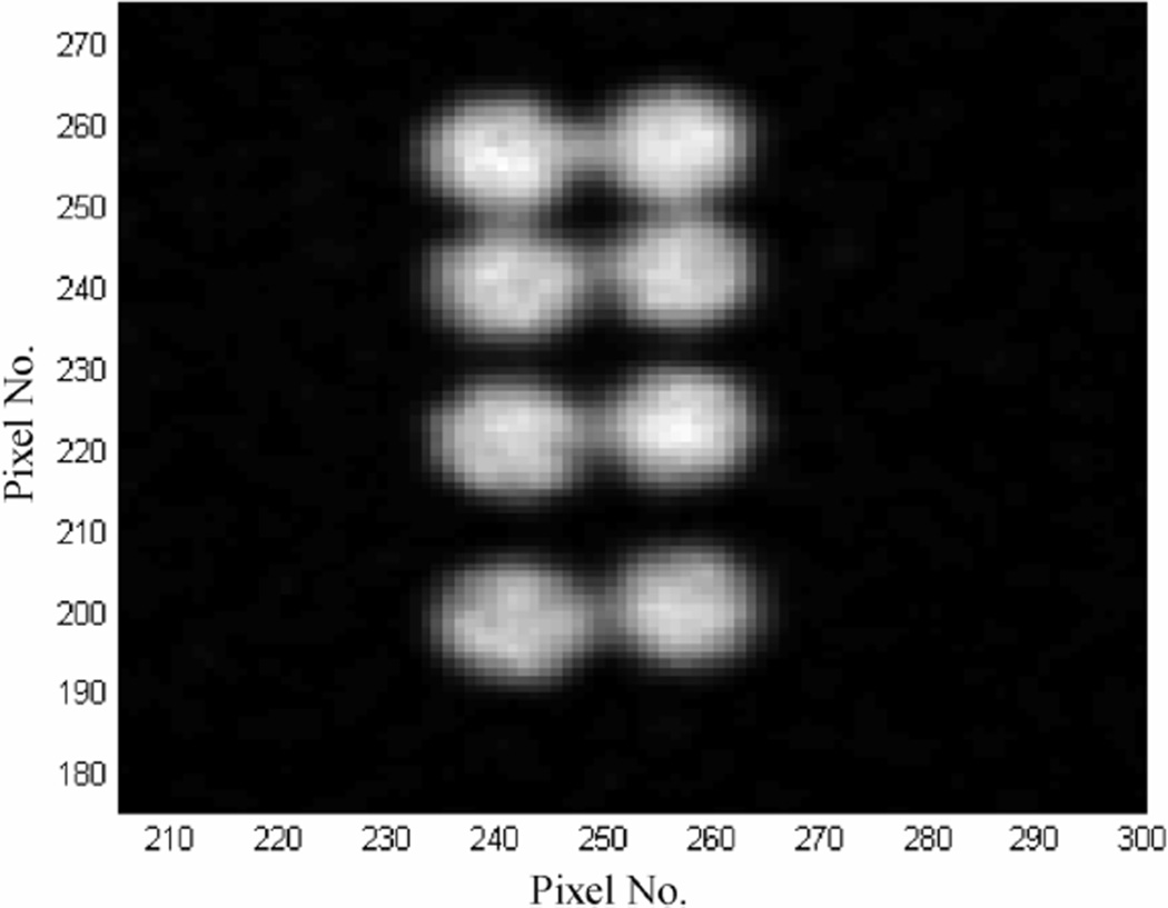
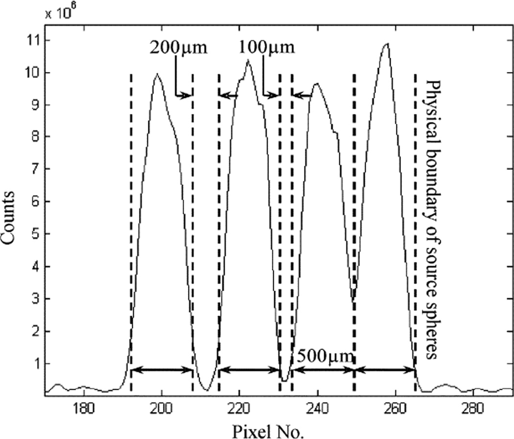
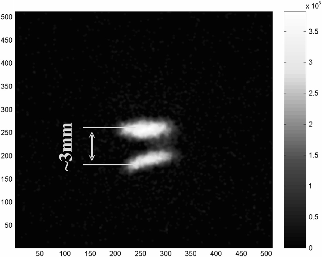
To further verify the performance of this detector, we tested it with a micro pinhole aperture for some planar imaging studies. The aperture has a single pinhole of 100 µm diameter. The experimental setup is shown in Fig. 7. The first set of measurements was made using a planar scene containing multiple spherical objects of 500 µm diameter. The source sphere to pinhole distance was ~2 cm and the pinhole was 2cm away from the detector. Images were reconstructed in 2-D using the standard MLEM algorithm [33]. A reconstructed image containing two source spheres is shown in Fig. 8. For imaging at a very high resolution, it is difficult to find a true point (or line) source that has a physical dimension much smaller than the expected imaging resolution (< 100microns). To measure the imaging resolution, we used an indirect method based on fitting the reconstructed source object profile to the expected one. The latter is assumed to be the convolution of the true profile (known a priori) with a Gaussian blurring. Knowing that the source sphere has an exact size of 500 µm diameter, the width of the Gaussian blurring was determined to be ~75 µm FWHM. This fitting process is illustrated in Fig. 9. To further verify this result, we used a planar phantom with 8 source spheres divided into 4 pairs. The dead spaces between pairs are 0 µm, 100 µm and 200 µm, respectively. The reconstructed 2-D image is shown in Figs. 10 and 11. From the cross section profile that cuts through the centers of the four spheres on the left hand side, we see that even without spacing, two closely packed source spheres can be nicely resolved. Two source spheres that are 100 µm apart were almost perfectly separated. These results confirmed that for the planar imaging case, an imaging resolution well below 100 µm can be achieved with the intensified EMCCD camera and a micro pinhole aperture. We also used this prototype pinhole camera to image the thyroid of a mouse, 24 hours after injecting 500 µCi I-125 solution. The actual uptake of the thyroid was measured (using a calibrated Anger camera) to be ~50 µCi. The anethesized mouse was placed in front of the camera with its thyroid 2 cm away from the pinhole. The data was acquired for 2 hours. A reconstructed image is shown in Fig. 12.
Fig. 7.
Experimental setup for preliminary imaging studies.
Fig. 8.
Reconstructed images with two spherical sources of 500 µm diameter. The center-to-center distance was also 500 µm.
Fig. 9.
Indirect determination of imaging spatial resolution with least squares fitting to the measured source profile.
Fig. 10.
Reconstructed image with eight spherical source objects of 500 µm diameter. The actual spacing between pairs are 0 µm, 100 µm and 200 µm, respectively.
Fig. 11.
1-D cross-section cutting through the centers of the four source spheres on the left hand side in Fig 10.
Fig. 12.
Reconstructed mouse thyroid image.
IV. Conclusions and Discussions
We presented the design and preliminary experimental evaluations of an ultra-high resolution gamma camera for I-125 image applications. This detector is based on a recently developed EMCCD sensor and a DM tube. Experimental results are summarized as below:
An ultra-high intrinsic resolution of ~60 µm FWHM was achieved for detecting 27–35 keV X and gamma rays emitted by I-125. There is plenty of room for further improving the spatial resolution to below 50 µm.
An excellent photon counting capability was demonstrated. True interactions can be detected with a very high efficiency and images are almost free of false positives caused by noise events from the DM/EMCCD readout chain.
The high readout speed of the EMCCD camera allows a frame rate of 30–100 frame/sec to be achieved along with a high spatial resolution. We expect that the camera is capable of handling several thousands of interactions per second, which should be sufficient for the SPEM system based on this detector.
An imaging resolution of <80 µm FWHM has been experimentally demonstrated in planar imaging case for image scenes that contain isolated “point-like” source objects only. This gamma camera offers a great potential for ultra-high resolution SPECT imaging.
Although an excellent performance has been demonstrated on the prototype detector, there is much room for further improvements. For example, the photoelectron yield on the DM tube can be greatly improved by using different scintillators or scintilator plates directly as the entrance window. These would lead to not only a much better energy resolution, but also further improved spatial resolution. We are actively working on refining the design of the DM tube to reduce the dead area, so multiple detectors can be packed closer. In principle, we can also use detectors with similar configuration for detecting gamma rays with higher energy (for example, the 140 keV gamma rays from Tc-99 m).
References
- 1.Wu MC, Hasegawa BH, Dae MW. Performance evaluation of a pinhole SPECT system for myocardial perfusion imaging of mice. Med. Phys. 2002;29:2830–2839. doi: 10.1118/1.1521939. [DOI] [PubMed] [Google Scholar]
- 2.McElroy DP, MacDonald LR, Beekman FJ, Wang YC, Patt BE, Iwanczyk JS, Tsui BMW, Hoffman EJ. Performance evaluation of A-SPECT: A high resolution desktop pinhole SPECT system for imaging small animals. IEEE Trans. Nucl. Sci. 2002 Oct.49(5):2139–2147. [Google Scholar]
- 3.Weisenberger AG, Kross B, Majewski S, Wojick R, Bradley EL, Saha MS. Design features and performance of a CsI(Na) array based gamma camera for small animal gene research. IEEE Trans. Nucl. Sci. 1998 Dec.45(6):3053–3058. [Google Scholar]
- 4.Weisenberger AG, Wojcik R, Bradley EL, Brewer P, Majewski S, Qian J, Ranck A, Saha MS, Smith K, Smith MF, Welsh RE. SPECT-CT system for small animal imaging. IEEE Trans. Nucl. Sci. 2003 Feb.50(1):74–79. [Google Scholar]
- 5.Beekman FJ, McElroy DP, Berger F, Gambhir SS, Hoffman EJ, Cherry SR. Towards in vivo nuclear microscopy: Iodine-125 imaging in mice using micro pinholes. Eur. J. Nucl. Med. Jul. 2002;29(7):933–938. doi: 10.1007/s00259-002-0805-6. [DOI] [PubMed] [Google Scholar]
- 6.Beekman FJ, Vastenhouw B, Van der Have F. Towards 3D nuclear microscopy using locally focusing many-pinhole SPECT; Proc. 2003 Meeting on Fully 3D Image Reconstruction in Radiology and Nuclear Medicine; [Online]. Available: www.fully3d.org. [Google Scholar]
- 7.Dilmanian FA, Weber DA, Coderre JA, Joel DD, Shi KC, Meinken GE, Som P, Tang YN, Volkow ND, Yee C, Brill AB, Watanabe M, Inuzuka E, Oba K, Gerson R, Iida H, Hiruma A. A high-resolution spect system based on a microchannel-plate imager. IEEE Trans. Nucl. Sci. 1990 Apr.37(2):687–695. [Google Scholar]
- 8.Karellas A, Hong L, Reinhardt C, Harris LJ, Brill AB. Imaging of radionuclide emissions with a low-noise charge-coupled-device. IEEE Trans. Nucl. Sci. 1993 Aug.40(4):979–982. [Google Scholar]
- 9.Beekerman FJ, Colijn AP, Vastenhouw B, Wiegant VM, Gerrits MAFM. High-resolution emission tomography of small laboratory animals: Physics and gamma-astronomy meet molecular biology. Nucl. Instrum. Methods Phys. Res. A. 2003;A509(1–3):229–234. [Google Scholar]
- 10.Beekman FJ, van der Have F, Vastenhouw B, van der Linden AJA, van Rijk PP, Burbach JPH, Smidt MP. U-SPECT-I: A novel system for submillimeter-resolution tomography with radiolabeled molecules in mice. J. Nucl. Med. 2005;46:1194–1200. [PubMed] [Google Scholar]
- 11.Peterson TE, Kim H, Crawford MJ, Hunter WCJ, Barber HB, Furenlid LR, Wilson DW, Barrett HH. SemiSPECT: A small-animal imaging system based on eight CdZnTe pixel detectorsin. Proc. IEEE Nuclear Science Symp. and Medical Imaging Conf. 2002;3:1844–1847. doi: 10.1109/NSSMIC.2002.1239682. [DOI] [PMC free article] [PubMed] [Google Scholar]
- 12.Kastis GA, Furenlid LR, Wilson DW, Peterson TE, Barber HB, Barrett HH. Compact CT/SPECT small-animal imaging system. IEEE Trans. Nucl. Sci. 2004 Feb.51(1):63–67. doi: 10.1109/TNS.2004.823337. [DOI] [PMC free article] [PubMed] [Google Scholar]
- 13.Beekman FJ, Vastenhouw B. Design and simulation of a high-resolution stationary SPECT system for small animals. Phys. Med. Biol. 2004;49(19):4579–4592. doi: 10.1088/0031-9155/49/19/009. [DOI] [PubMed] [Google Scholar]
- 14.Beekman FJ, de Vree GA. Photon-counting versus an integrating CCD-based gamma camera: Important consequences for spatial resolution. Phys. Med. Biol. 2005;50:N109–N119. doi: 10.1088/0031-9155/50/12/N01. [DOI] [PubMed] [Google Scholar]
- 15.de Vree GA, Westra AH, Moody I, van der Have F, Ligtvoet KM, Beekman FJ. Photon-counting gamma camera based on an electron- multiplying CCD. IEEE Trans. Nucl. Sci. 2005 Jun.52(3):580–588. [Google Scholar]
- 16.Choong WS, Moses WW, Tindall CS, Luke PN. Design for a high-resolution small-animal SPECT system using pixellated Si(Li) detectors for in vivo I-125 imaging. IEEE Trans. Nucl. Sci. 2005 Feb.52(1):174–180. [Google Scholar]
- 17.Peterson TE, Wilson DW, Barrett HH. Application of silicon strip detectors to small-animal imaging. Nucl. Instrum. Methods Phys. Res. A. 2003;A505:608–611. [Google Scholar]
- 18.Meng LJ. Design and feasibility study of a single photon emission microscope system for small animal I-125 imaging. IEEE Trans. Nucl. Sci. 2006 Jun.53(3):1168–1178. doi: 10.1109/TNS.2006.871405. [DOI] [PMC free article] [PubMed] [Google Scholar]
- 19.Meng LJ. A single photon emission microscope system for small animal I-125 imaging. presented at the IEEE NSS/MIC; Puerto Rico. 2005. [DOI] [PMC free article] [PubMed] [Google Scholar]
- 20.Vessotskie JM, Kung MP, Chumpradit S, Kung HF. Quantitative autoradiographic studies of dopamine D3 receptors in rat cerebellum using [I-125]S(-)5-OH-PIPAT. Brain Res. 1997;778:89–98. doi: 10.1016/s0006-8993(97)01014-7. [DOI] [PubMed] [Google Scholar]
- 21.Kung MP, Canney DJ, Frederick D, Zhuang Z, Billings JJ, Kung HF. Binding of I-125 iodovinyltetrabenazine to Cns vesicular monoamine transport sites. Synapse. 1994;18:225–232. doi: 10.1002/syn.890180308. [DOI] [PubMed] [Google Scholar]
- 22.Burris KD, Flitz TM, Chumpradit S, Kung MP, Foulon C, Hensler JG. Characterization of [I-125] (R)Trans-7-Hydroxy-2-[N-Propyl-N-(3’-Iodo-2’-Propenyl) Amino] tetralin binding to dopamine D3 receptors in rat olfactory tubercle. J. Pharmacol Exp. Ther. 268:935–942. I994. [PubMed] [Google Scholar]
- 23.Coates C, Denvir D, Haron I, Hollywood M, Thornbury K, McHale N. EMCCD—The definitive ultra low-light solution? Biophys. J. 2004;86(1):151a–151a. [Google Scholar]
- 24.Robbins MS, Hadwen BJ. The noise performance of electron multiplying charge-coupled devices. IEEE Trans. Electron Devices. 2003;50(5):1227–1232. [Google Scholar]
- 25.Nagarkar V, Shestakova I, Gaysinskiy V, Tipnis SV, Singh B, Barber WC, Hasegawa BH, Entine G. CCD-based detector for SPECT; IEEE NSS-MIC Conf. Rec; Rome, Italy. 2004. [Google Scholar]
- 26.Technical Datasheet. [Online]. Available: www.photek.com. [Google Scholar]
- 27.CCD97 Back Illuminated Datasheet. [Online]. Available: http://e2vtechnologies.com/product_guides/l3vision_sensors.htm. [Google Scholar]
- 28.Frojdh C, Nilsson HE, Nelvig P, Petersson CS. Simulation of the X-ray response of scintillator coated silicon CCDs. IEEE Trans. Nucl. Sci. 1998 Jun.45(3):374–378. [Google Scholar]
- 29.Robbins MS, Hadwen BJ. The noise performance of electron multiplying charge-coupled devices. IEEE Trans. Electron Devices. 2003 May;50(5):1227–1232. [Google Scholar]
- 30.van Loef EVD, Dorenbos P, van Eijk CWE, Kramer K, Gudel HU. High-energy-resolution scintillator: Ce3+ activated LaBr3. Appl. Phy. Lett. 2001;79:1573–1575. [Google Scholar]
- 31.D’Ambrosio C, De Notaristefani F, Leutz H, Puertolas D, Rosso E. X-ray-sensitive hybrid photon detectors with Be-windows. IEEE Trans. Nucl. Sci. 2005 Jun.52(3):729–735. [Google Scholar]
- 32.Pani R, Cinti MN, Pellegrini R, De Notaristefani F, Bennati P, Betti M, Trotta G, Mattioli M, Garibaldi F. LaBr3:Ce scintillation camera. presented at the IEEE NSS/MIC; Puerto Rico. 2005. [Google Scholar]
- 33.Shepp LA, Vardi Y, Ra JB, Hilal SK, Cho ZH. Maximum-likelihood pet with real data. IEEE Trans. Nucl. Sci. 1984;NS-31:910–913. [Google Scholar]


