Abstract
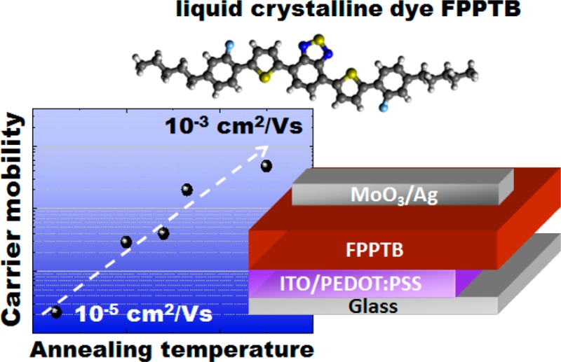
We investigated the influence of molecular packing on the optical and electrical properties of the liquid crystalline dye 4,7-bis[5-(2-fluoro-4-pentyl-phenyl)-2-thienyl]-2,1,3-benzothiadiazole (FPPTB). FPPTB is crystalline at room temperature, exhibits a nematic phase at temperatures above 149 °C and is in an isotropic melt at temperatures above 230 °C. Solution processed FPPTB films were subject to thermal annealing through these phase transition temperatures and characterized with X-ray diffraction and polarized optical microscopy. Cooling FPPTB films from the nematic and isotropic phases increased crystal domain size, but also induced local structural variations in the molecular packing of crystalline FPPTB. The decrease in long-range order was correlated with an increase in short-range π–π interactions, leading to changes in molecular aggregation which persisted even when the FPPTB films were cooled to room temperature. Annealing-induced changes in molecular aggregation were confirmed with optical spectroscopy. The carrier mobility in FPPTB films increased over 2 orders of magnitude from (2.2 ± 0.4) × 10–5 cm2 V–1 s–1 in as-spun films to μ = (5.0 ± 0.8) × 10–3 cm2 V–1 s–1 in films cooled from the isotropic melt. We discuss the relationship between thermal stability and high carrier mobility values in terms of the interplay between long-range molecular order and increased π–π interactions between molecular pairs in the FPPTB film.
Keywords: liquid crystal, dye, organic semiconductor, mobility, molecular packing, thermal stability
Introduction
Organic semiconductors have great potential in novel electronic applications because of the endless possibilities to create new materials that can be processed in large scale at low cost. The major bottleneck for developing high-performance organic electronics is the compromise between increasing charge carrier mobility while maintaining good processability, ideally in nontoxic solvents. Enhancing the solubility of small molecules generally comes at the expense of the structural integrity and thermal stability of the resulting film.1−4
Conjugated liquid crystals (LCs) offer many advantages in this regard. LCs are associated with low molecular weights, high chemical purity and molecular self-assembly resulting in highly ordered thin films.5,6 Disc-like (discotic)7−10 LCs form ordered one-dimensional columns with excellent π – π stacking; however, carrier transport is limited by structural defects in the one-dimensional, columnar structures. Rod-like (calamitic) LCs, on the other hand, form two-dimensional ordered layered films.5 Carrier transport is more robust against structural defects in calamitic LC films11 than in discotic LC films, however, overlap between the π orbitals of neighboring molecules is also more limited.7 Carrier mobility can be optimized in calamitic LC films by slowly cooling the film through progressively ordered smectic phases12−14 to optimize π–π stacking and reduce structural defects in the film. Recently, field effect mobility values exceeding 10 cm2 V−1 s−1) were demonstrated with LC films exhibiting a highly ordered smectic E phase.4
Although discotic LCs and conducting polymer LCs15 have been investigated in optoelectronic applications,16,17 few studies have focused on small molecule LC dyes.18 In this study, we synthesized the novel calamitic LC dye 4,7-bis[5-(2-fluoro-4-pentyl-phenyl)-2-thienyl]-2,1,3-benzothiadiazole (FPPTB). FPPTB combines the advantages of good chemical purity, tunable absorption and emission properties for optoelectronic applications, and flexible processability. We exploit the molecular ordering properties of FPPTB to fabricate crystalline organic thin films. Studies of the structural, optical and electrical properties of the films reveal increased π–π interactions in the nematic phase and isotropic melt that persist after cooling of the films into the crystalline phase. These interactions are observed to be correlated with the good thermal stability and high carrier mobility values observed in annealed FPPTB films.
Results and Discussion
Structure and Properties of FPPTB
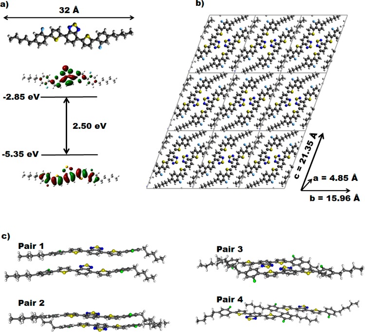
Figure 1a shows the molecular structure of FPPTB. The calculated highest occupied molecular orbital (HOMO) and lowest unoccupied molecular orbital (LUMO) are −5.35 and −2.85 eV, respectively, yielding an optical band gap of FPPTB 2.50 eV (496 nm). From the geometry of the HOMO and LUMO orbitals, we observe that the hole wave function is delocalized over the conjugated backbone while the electron wave function is localized on the benzothiadiazole acceptor unit.
Figure 1.
(a) molecular structure and the calculated highest occupied molecular orbital (HOMO) and lowest unoccupied molecular orbital (LUMO) of FPPTB; (b) triclinic lattice of FPPTB showing 9 unit cells depicted in the (100) direction; (c) four nearest molecular pairs in the crystal.
From X-ray diffraction (XRD) patterns taken from single crystals of FPPTB, the unit cell was determined to be triclinic with the lattice parameters a = 4.85 Å, b = 15.96 Å, c = 21.35 Å and α = 69.86°, β = 85.97°, and γ = 86.59°. Details of the synthesis and XRD analysis can be found in the Experimental Section. The simulated and experimentally measured powder XRD patterns can be found in the Supporting Information. The crystal structure in the (100) direction is shown in Figure 1b and the relative positions of the four nearest neighbors in the FPPTB crystal are shown in Figure 1c.
Electronic transport in organic semiconductors is commonly described using Marcus theory,19 which predicts the electron transfer rate ket between molecules A and B according to
| 1 |
where λ is the reorganization energy, J is the transfer integral, h is Planck’s constant, k is Boltzmann’s constant, and T is temperature. The electron transfer rate ket is determined by molecular reorganization energy (λ) upon charge transfer as well as the overlap of electronic orbitals between neighboring molecules (J). The transfer integral J, in turn, is determined by intermolecular distance and orientation as well as variations in molecular conformation.20 We calculated the transfer integrals for holes (J+) and electrons (J−) for the molecular pairs in the FPPTB crystal. The results are summarized in Table 1.
Table 1. Values for the Transfer Integral J for Electrons (J−) and Holes (J+) for the Four Nearest Pairs in the FPPTB Crystal.
| J+ (meV) | J– (meV) | |
|---|---|---|
| pair 1 | 65 | 35 |
| pair 2 | 8 | 11 |
| pair 3 | 2 | 69 |
| pair 4 | 1 | 7 |
FPPTB exhibits good solubility in common organic solvents, such as chloroform, chlorobenzene, dioxane, toluene, and THF. We obtained the best reproducibility for film processing in THF. Figure 2 shows the absorption (black line) and emission spectra (red and blue lines) of FPPTB in dilute THF solution. The absorption spectrum exhibits two peaks, and the molar extinction coefficient of FPPTB was found to be 40 000 M–1 cm–1 at 345 nm and 29 000 M–1 cm–1 at 491 nm. The maximum at 491 nm agrees with the calculated optical bandgap of FPPTB of 496 nm. The emission spectrum is red-shifted with respect to the absorption spectrum and centered at 610 nm. We did not observe any dependence of the fluorescence spectra on excitation wavelength, and emission spectra taken for excitation at 350 and 480 nm are shown.
Figure 2.
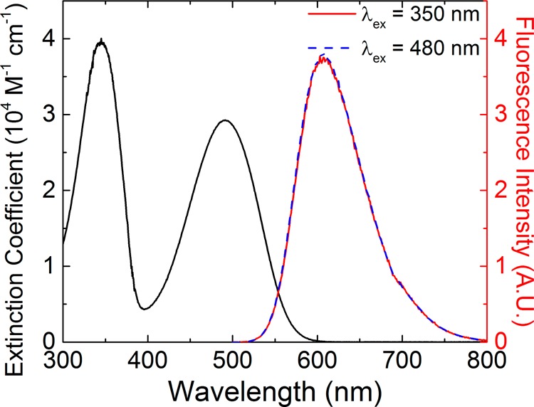
Absorption spectrum (black line) and emission spectra taken at excitation wavelengths of 350 nm (red line) and 480 nm (blue line) of FPPTB in solution (THF).
The phase transition temperatures (and enthalpies) of FPPTB were determined with differential Scanning Calorimetry (DSC) and found to be crystalline → nematic 149.0 °C (7000 cal/mol), nematic → isotropic 229.7 °C (200 cal/mol).
Molecular Packing in FPPTB Films
We studied the temperature-dependent molecular packing of FPPTB thin films to determine the influence of intermolecular interactions and molecular interactions with the substrate21 on the phase transition temperatures and film structure. Normalized XRD patterns taken from a FPPTB film during heating and cooling are depicted in Figure 3a, b, respectively. The temperature of the sample was changed at a rate of 30 °C/min for both heating and cooling cycles. As-spun FPPTB films demonstrate a weak peak at 2θ = 2.72, which corresponds to a lattice spacing of 32.5 Å. This value is consistent with the length of the FPPTB molecule. This indicates that although FPPTB is crystalline at room temperature, spin-casting FPPTB films does not enable film formation consistent with the packing structure shown in Figure 1b. Instead, as-spun films demonstrate head-to-head molecular stacking. When the film is heated to 70 °C, an additional peak at 2θ = 4.14 (lattice spacing of 21.3 Å) is observed. At 100 °C a prominent peak at 2θ = 3.77 (lattice spacing of 23.46 Å) emerges, whereas the intensity of the peak at 4.14 (lattice spacing of 21.3 Å) decreases and the peak at 2θ = 2.72 disappears. At 140 °C, the peak at 2θ = 3.77 (lattice spacing of 23.46 Å) is the most prominent, and a second weaker peak at 2θ = 7.54 is observed. This peak, hardly visible in Figure 3a, is shown in higher magnification in Figure 4b. This pair of peaks is consistent with the (001) and (002) planes (Figure 1b) (see the Supporting Information). This indicates the formation of highly ordered FPPTB molecular layers oriented parallel to the substrate, with the c-axis of the unit cell oriented perpendicular to the substrate at temperatures between 100 and 140 °C. At 155 °C, we do not observe any peaks associated with crystalline structure, indicating the film is in the nematic phase at this temperature.
Figure 3.
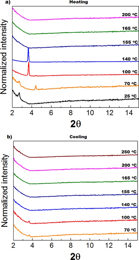
In situ XRD patterns of an FPPTB film taken during (a) heating and (b) cooling.
Figure 4.
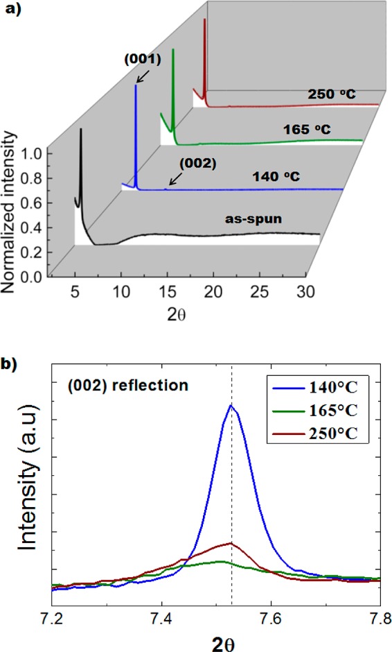
(a) Normalized XRD patterns of as-spun FPPTB (black), and FPPTB films annealed at 140 °C (blue), 165 °C (green), and 250 °C (wine); (b) zoom into the (002) reflection of the XRD patterns of FPPTB films annealed at 140 °C (blue), 165 °C (green), and 250 °C (wine).
During the cooling cycle, no peaks associated with the crystal structure are observed in spectra taken between 250 and 140 °C (Figure 3b). This indicates that the film is still in the nematic phase at 140 °C during cooling. Peaks associated with the crystal structure first emerge in spectra taken at 100 and 70 °C, but with reduced relative intensity compared to the heating cycle.
We next investigated the effect of cooling from the different phases (crystalline, nematic and isotropic) on molecular packing in FPPTB films at room temperature. As-spun FPPTB films (crystalline phase), and FPPTB films annealed at 140 °C (just below the transition from the crystalline phase to the nematic phase), 165 °C (nematic phase) and 250 °C (isotropic melt) were prepared and the FPPTB films were characterized after cooling to room temperature (crystalline phase). Figure 4a shows the normalized XRD patterns of an as-spun FPPTB film (black) and FPPTB films annealed at 140 °C (blue), 165 °C (green), and 250 °C (wine). The spectrum from the as-spun film is consistent with the spectrum of the as-spun film in Figure 3a, and demonstrates signatures of head to head stacking of FPPTB molecules. Annealed FPPTB films, on the other hand, yield XRD peaks consistent with molecular crystal packing depicted in Figure 1b, and we observe the 2θ peaks corresponding to the (001) and (002) crystal planes. FPPTB films annealed at 140 °C demonstrate the most prominent and narrow peaks. In contrast, FPPTB annealed at 165 °C (nematic phase) and 250 °C (isotropic melt) show a slight shift in the peaks, and the (001) peak shifts from 2θ = 3.77 to 2θ = 3.74, corresponding to a slight increase in the lattice spacing from 23.46 to 23.59 Å. In addition the relative intensity of both the (001) and (002) peaks decreases, and the peaks broaden. This effect is illustrated in Figure 4b shows the zoom in of the XRD pattern centered on the (002) peak. Shifting of molecules in the unit cell relative to nearest neighbors induces variations in local order (resulting in peak broadening) as well as a change in the dimensions of the unit cell (resulting in peak shifting).
Polarized optical microscopy images of the FPPTB films as-spun as well as those annealed at 140, 165, and 250 °C are shown in Figure 5a–d, respectively. All of the films are crystalline and the size of the crystal domains increases with annealing temperature.
Figure 5.
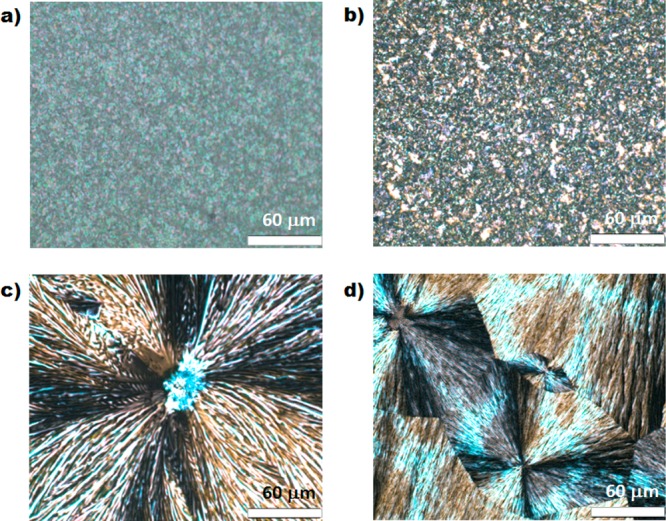
Polarized optical microscopy images of (a) as-spun FPPTB and FPPTB films annealed at (b) 140, (c) 165, and (d) 250 °C.
Obtaining crystalline films with LC materials generally requires cooling through ordered smectic phases to avoid grain boundaries, cracking and droplet formation due to dewetting.4,13 Despite the lack of a smectic phase for FPPTB, we observe excellent film coverage (Figure 5) and structural integrity even for films that were cooled from the isotropic melt. We attribute this to increased short-range intermolecular interactions in the nematic phase and isotropic melt. This leads to asymmetric heating and cooling behavior; the transition between the nematic and crystalline phase occurs at lower temperatures during film cooling than film heating. During cooling, the intermolecular interactions promote local molecular displacement in the crystal packing, as evidenced by broadening and shifting of the (001) and (002) signatures (Figure 4b). As a result, slow cooling from the nematic phase (165 °C) and the isotropic melt (250 °C) promotes the formation of large domains with local structural defects in the molecular packing structure, compared to FPPTB films annealed in the crystalline phase (140 °C).
The difference in the temperature of the transition from crystalline → nematic during heating, and nematic → crystalline during cooling is advantageous for realizing thermally stable organic films for device applications.4 FPPTB films can be deposited and processed in a wide temperature window, allowing for more flexibility in film fabrication. At the same time, FPPTB film structure and integrity is maintained at elevated operating temperatures (up to 140 °C).
Optical Properties
Emission spectra of as-spun FPPTB films (black squares) and FPPTB films annealed at 100 °C (red triangles), 140 °C (blue circles), 165 °C (green stars) and 250 °C (wine crosses) are shown in Figure 6a. We observe that emission yield is highest in FPPTB films with ordered packing structure (140 and 100 °C), intermediate in FPPTB films which exhibit variations in local molecular packing (165 and 250 °C), and lowest in FPPTB films with reduced long-range order (as-spun).
Figure 6.
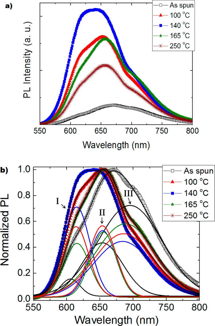
(a) Emission spectra of as-spun FPPTB films (black squares) and FPPTB films annealed at 100 °C (red triangles), 140 °C (blue circles), 165 °C (green stars), and 250 °C (wine crosses). (b) Normalized emission spectra from the FPPTB films fit with three Gaussian distributions, denoted as the I, high energy; II, intermediate energy; and III, low energy contributions, respectively.
To gain more insight into the role of molecular packing on the emission line shape we investigated the normalized spectra (Figure 6b). We observe that emission line shape is dependent on annealing conditions, although films annealed at 165 °C (nematic) and 250 °C (isotropic) exhibit identical spectral form when normalized.
Gas-to-crystal shifts in the optical spectra of crystalline organic films are determined by variations in packing structure as well as localized, site-dependent interactions, which can lead to distinct features in the spectra.22 We fit the emission spectra from the FPPTB films as a combination of three Gaussian distributions, which we denote as the I, high energy; II, intermediate energy; and III, low energy contribution, respectively. We used this simple model to fit all the spectra, and the peak position of the Gaussian distributions were free fitting parameters. We found that the peak positions of the three distributions are nearly identical for all samples, and that the relative intensity of each distribution determined the spectral line shape.
The high energy feature I is centered at 605 nm for the as-spun FPPTB film and broadens and shifts to 615 nm for all the annealed films. The intensity is highest in FPPTB films annealed in the crystalline phase (100 and 140 °C), lower in FPPTB annealed at in the nematic phase (165 °C) and isotropic melt (250 °C) and lowest in as-spun FPPTB films. The peak position of this feature is slightly red-shifted from the monomer emission in solution (600 nm), and we attribute this feature to monomer-like emission from molecules in bulk FPPTB crystallites. Quenching of emission from this feature is consistent with reduced long-range crystal order (as-spun FPPTB) as well as local changes in FPPTB packing (FPPTB annealed at 165 and 250 °C).
The intermediate energy feature II is centered at 653 nm, and we do not observe a change in peak position with annealing. The intensity is lowest and the distribution is the broadest in the PL spectrum from the as-spun film. The width of this distribution is identical for the annealed FPPTB films, and the relative intensity varies only slightly between the PL spectra taken from these samples. We attribute this feature to coupling between molecular pairs in bulk FPPTB crystallites (Figure 1b, c).
Finally we consider the low energy feature III. The relative intensity and peak position of this feature show the most dependence on annealing conditions of all three features. The relative intensity is the highest for the as-spun FPPTB film (695 nm) and lowest for the FPPTB film annealed at 140 °C (684 nm). The increase in peak intensity and width, as well as the red-shifting of peak position of the Gaussian feature directly correlate with reduced long-range molecular order in the films. For this reason, we tentatively attribute changes in this feature to variations in short-range coupling between molecular pairs in the FPPTB crystal.
Electrical Properties
The geometry of the FPPTB HOMO (Figure 1) indicates that the hole wave function is delocalized over the conjugated backbone and hole transport occurs via π–π overlap between neighboring molecules. FPPTB forms stacked layers running perpendicular to the substrate, and transport is limited by charge transfer between layers. The geometry of the LUMO, on the other hand, indicates that electron transfer is determined primarily by alignment of the benzoldithiazole acceptor units between molecular pairs. Shifts in molecular pairs can increase lateral electron mobility along the (100) and (010) direction. For carrier transport in FPPTB diodes, however, changes in molecular placement along the direction of transport, i.e., along the c-axis, are most relevant. For this reason, we focus on studying hole transport in FPPTB. “Hole only” diodes were prepared according to the details in the Experimental Section.
The current density–voltage (JV) characteristics are shown in Figure 7 for diodes prepared with as-spun FPPTB films (black squares) and FPPTB films annealed at 140 °C (blue circles), 100 °C (red triangles), 165 °C (green stars), and 250 °C (wine crosses). The current density of annealed FPPTB is higher than in as-spun FPPTB films, and current density increases with increasing annealing temperature. Diodes prepared with FPPTB films annealed at 100 and 140 °C demonstrate very similar JV characteristics, whereas FPPTB annealed at 250 °C has the highest current density of all samples.
Figure 7.
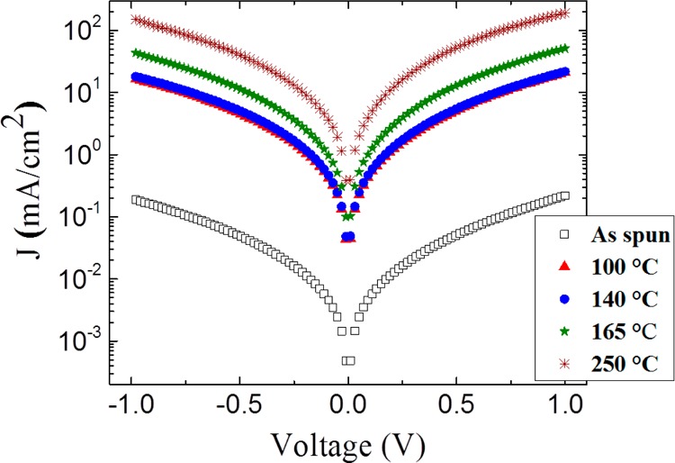
Current density–voltage (JV) characteristics for diodes prepared with as-spun FPPTB films (black squares) and FPPTB films annealed at 140 °C (blue circles), 100 °C (red triangles), 165 °C (green stars), and 250 °C (wine crosses).
We performed impedance spectroscopy in order to understand the electrical properties of FPPTB in more detail. In particular we investigated how annealing influences film resistance and dispersive transport phenomena. Liquid crystalline semiconductors generally demonstrate narrow energetic distributions for electronic transport with reduced trapping and limited or no dispersive transport.11 Structural and chemical defects, however, cause dispersive carrier transport23 manifested as voltage-dependent mobility values.9
The Nyquist plots (−Z″ versus Z′) from the impedance data taken over a frequency range between 1 MHz and 10 Hz are shown in Figure 8a. The experimental (symbols) data were taken at a DC offset of 0 V and fit with an equivalent circuit model (lines). The impedance values are much higher for diodes prepared with as-spun FPPTB films, so for clarity, Figure 8a shows all the data, whereas Figure 8b depicts a zoom-in of the impedance data from the diodes prepared with annealed films (100 °C – red triangles, 140 °C, blue circles; 165 °C, green stars; and 250 °C, wine crosses). We applied a simple equivalent circuit to model the data, consisting of a series resistance (Rs) and a resistor (Rp) in parallel with a constant phase element (CPE). The equivalent circuit diagram is shown in the inset of Figure 8a. Rs is determined by the contact resistance of the device, and is therefore frequency-independent and comparable between samples. The values of the Rp–CPE element are determined by the electrical properties of the FPPTB film. Details about the equivalent circuit model, and the corrrelation between Rp and carrier mobility in the FPPTB films are given in the Supporting Information.
Figure 8.
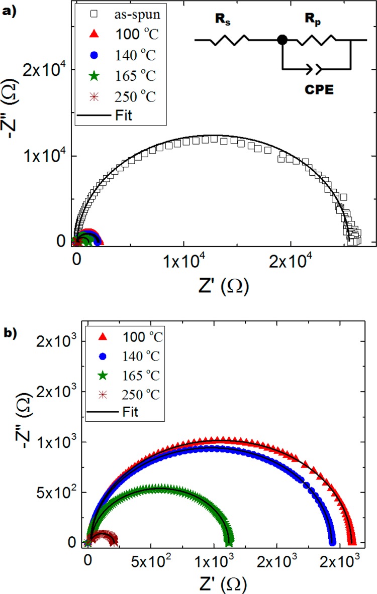
(a) Nyquist plots (−Z″ versus Z′) from the impedance data taken over a frequency range between 1 MHz and 10 Hz). (b) Zoom-in of the impedance data from the diodes prepared with annealed films (100 °C, red triangles; 140 °C −, blue circles; 165 °C, green stars; and 250 °C, wine crosses).
CPE values depend on the frequency-dependent capacitance of the film. Specifically, the CPE accounts for nonidealities in the device capacitance, i.e., dispersive transport. The impedance of the CPE is given by
| 2 |
where Qo is the impedance of the CPE at low frequency (1 rad/s), and n is a dimensionless parameter between 0 and 1. If n = 1, the CPE reduces to an ideal capacitor and if n = 0, the CPE reduces to an ideal resistor. The values of the circuit elements, along with the annealing temperatures for each sample, are summarized in Table 2. We note that the value of n for all of the samples was between 0.98 (as-spun FPPTB) and 0.99 (annealed FPPTB) indicating nearly ideal capacitive behavior, and negligible dispersive transport, independent of annealing conditions. The capacitive value of the CPE element (taken at ω = 1 rad/s) varies slightly between the samples, from 3.46 to 5.84 nF, and no trend with annealing is observed. The most significant difference between the electrical properties of the FPPTB films is the decrease in Rp with annealing temperature, from 25 400 Ω (as-spun FPPTB) to 188 Ω (FPPTB annealed at 250 °C). The decrease in FPPTB film resistance with annealing temperature is consistent with the increase in crystal domain size observed in Figure 5, i.e., the decrease in grain boundaries in the film.
Table 2. Values for Circuit Elements (Rs, R and Qo) dor Diodes Prepared with FPPTB Which Was Not Annealed, and Annealed at 100, 140, 165,and 250 °C.
| Annealing Temperature (°C) | RS (Ω) | R (Ω) | Qo At Ω = 1 Rad/S (Nf) | N |
|---|---|---|---|---|
| As-Spun | 21.7 | 25400 | 3.46 | 0.98 |
| 100 | 19.7 | 2072 | 4.48 | 0.99 |
| 140 | 23.2 | 1910 | 3.38 | 0.99 |
| 165 | 25.9 | 1094 | 3.34 | 0.99 |
| 250 | 19.7 | 188 | 5.84 | 0.99 |
Figure 9a shows the Bode plots for −Z″ versus f spectra for the samples. The charge carrier mobility μ can be determined from these data according to24−26
| 3 |
where d is the film thickness, VDC is the applied DC voltage offset, fo is the peak frequency of the −Z″ vs f spectra, and κ is a numerical factor that relates the time constant τc from the frequency-dependent data to the DC transit time of charge τDC. The value of κ is not clearly defined in the literature; however, Tsang et al.25 demonstrated that for organic materials with low dispersion τDC = 0.56τc.
Figure 9.
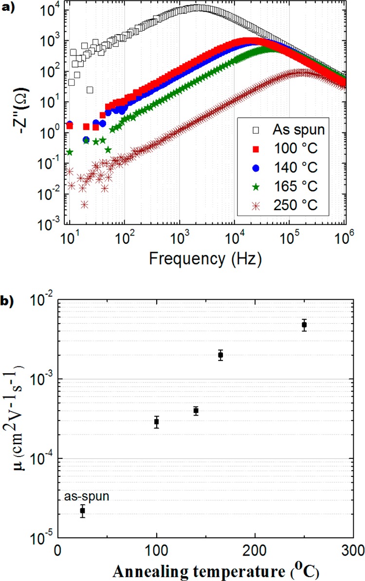
(a) Bode plots for −Z″ versus f spectra for the samples of FPPTB with annealed films (100 °C, red triangles; 140 °C, blue circles; 165 °C, green stars; and 250 °C, wine crosses) and (b) carrier mobility in FPPTB versus annealing temperature.
The hole mobility values versus annealing temperature are shown in Figure 8b. Carrier mobility increases over 2 orders of magnitude from μ = (2.2 ± 0.4) × 10–5 cm2 V–1 s–1 in as spun films to μ = (5.0 ± 0.8) × 10–3 cm2 V–1 s–1 in films annealed at 250 °C. We observe no voltage dependence in the carrier mobility, consistent with nondispersive transport.
We consider the increase in carrier mobility with annealing temperature in terms of the interplay between long-range crystalline order and short-range π- π interactions in FPPTB films. We observe that crystal domain size in FPPTB films (Figure 5a–d) increases with annealing temperature, corresponding to a decrease in the density of grain boundaries in the film. This is consistent with a decrease in FPPTB film resistance Rp and an increase in carrier mobility.27,28 However, annealing FPPTB at higher temperatures also induces local variations in molecular packing. This is evidenced by slight increase in the unit cell along the (001) plane and increased emission quenching in films annealed in the nematic phase and isotropic melt.
Local shifts in molecular position will influence the overlap of the electronic wave function between molecular pairs, and therefore the electron transfer rate.20,29 In particular, changes in intermolecular distances in the crystal packing structure that are mediated by short-range π–π interactions may lead to smaller intermolecular distances and increased electron transfer rates. Relative slipping of molecules in the (100) and (010) planes, corresponding to increased π–π interactions between molecular pairs 2–4, would promote increased two-dimensional hole transfer through the films.29,30 This is consistent with the increase in carrier mobility that we observe when cooling FPPTB films from the nematic phase and isotropic melt, which in turn is correlated with a decreased density of grain boundaries in the films.
Conclusions
We investigated the novel calamitic LC dye FPPTB. FPPTB is easily processed from solution and forms crystalline films at temperatures below 149 °C, exhibtis a nematic phase at temperatures between 149 and 230 °C, and is isotropic at temperatures above 230 °C. XRD and luminescence data revealed that annealing FPPTB films at temperatures just below the crystalline → nematic transition (140 °C) yielded films with the best crystalline order. Cooling FPPTB films from the nematic phase and isotropic melt led to decreased density of grain boundaries in the films. However, evidence of local structural defects in the crystal packing were observed in the XRD patterns and emission spectra from these films, and was attributed to increased short-range coupling between molecular pairs at higher temperatures which persisted upon cooling the films to the crystalline phase. Carrier mobility was observed to increase over 2 orders of magnitude with annealing, from μ = (2.2 ± 0.4) × 10–5 cm2 V–1 s–1 in as-spun FPPTB films to μ = (5.0 ± 0.8) × 10–3 cm2 V–1 s–1 in FPPTB films cooled from the isotropic melt. The resultant correlation between charge carrier mobility and annealing is explained by an interplay between long- and short-range order interactions in these three-dimensional structures. These results demonstrate that for LCs such as FPPTB, judicious choice of processing conditions can be used to tune electronic parameters for targeted device design.
Experimental Section
FPPTB Synthesis
The reaction was conducted under nitrogen atmosphere. The intermediates 2(31) and 3(32) were prepared as described in the literature.
1 (FPPTB)
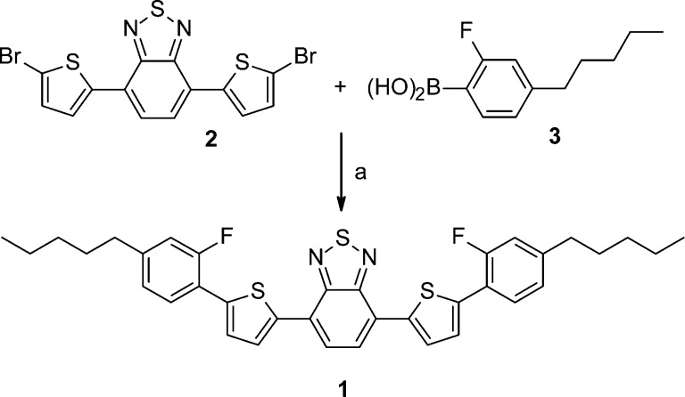
A solution of 2 (1.80 g, 3.93 mmol), 3 (1.73 g, 8.25 mmol), and Aliquat 336 (0.50 g, 1.24 mmol) in a mixture of toluene (60 mL) and 2 M aqueous Na2CO3 (15.7 mL, 31.4 mmol) was carefully degassed and then treated with tris(dibenzylideneacetone)dipalladium(0) (36 mg) and tris(o-tolyl)phosphine (48 mg). The mixture was refluxed for 18 h. After cooling, the organic phase was separated, and the aqueous layer extracted with 100 mL of toluene. The combined organic phases were dried with Na2SO4 and filtered with toluene over a short silicagel column. The red product fractions were evaporated to dryness. The crude product (1.9 g) was dissolved in hot toluene (25 mL), filtered, and crystallized at 8 °C to furnish 1 (1.7 g, 69%; 99.6% purity by HPLC) as red crystals (see Scheme 1).
Scheme 1. Synthesis of 1.
cat. [Pd2(dba)3], cat. (o-tolyl)3P, 0.3 equiv. of Aliquat 336, toluene, 2 M aqu. Na2CO3; reflux, 18 h (69%).
1H NMR (500 MHz, CDCl3, 303 K): δ = 8.11 (dd, J = 4.0, 0.8, 2H), 7.87 (s, 2H), 7.62 (t, J = 8.1, 2H), 7.52 (dd, J = 3.9, 1.2, 2H), 7.01 (s, 2H), 7.03–6.96 (m, 2H), 2.66–2.59 (m, 4H), 1.70–1.60 (m, 4H), 1.41–1.29 (m, 8H), 0.95–0.88 (m, 6H); 13C NMR (75 MHz, CDCl3, 303 K): δ = 157.47, 152.64, 144.94, 144.83, 138.87, 128.28, 128.24, 126.83, 126.74, 125.79, 125.42, 124.58, 124.53, 119.24, 116.27, 115.98, 77.17, 35.40, 31.37, 30.65, 22.47, 13.95; 19F NMR (282 Hz, CDCl3, 300 K): δ = −113.86 (dd, J = 12.4, 8.1, 2F); MS (EI, 70 eV): m/z (%) = 628 (100)[M+], 571 (20), 514 (15), 315 (5), 257 (17).
FPPTB Crystal Analysis
X-ray diffraction was performed on FPPTB single crystals (0.70 × 0.06 × 0.04 mm3). The unit cell is triclinic with space group P1̅, a = 4.8509(4) Å, b = 15.9558(8) Å, c = 21.3521(11) Å, α = 69.857(5)°, β = 85.974(6)°, γ = 86.590(5)°, V = 1546.64(16) Å3, Z = 2, ρcalcd = 1.350 g cm–3, linear absorption coefficient μ = 2.523 mm–1, λ = 1.54178 Å, T = 298 K, ω scans, 13464 reflections collected (−5 ≤ h ≤ 5; −18 ≤ k ≤ 16; −24 ≤ l ≤ 24), 4787 independent (Rint = 0.0607), 390 refined parameters, R = 0.0505, ωR2 = 0.1802, max. residual electron density 0.882 (−0.492) e Å–3. CCDC-1515128 contains the supplementary crystallographic data which can be obtained free of charge via the Internet (www.ccdc.cam.ac.uk/conts/retrieving.html) or from the Cambridge Crystallographic Data Centre, 12 Union Road, Cambridge CB2 1EZ, UK; fax: + 44 (1223) 336–033, E-mail: deposit@ccdc.cam.ac.uk.
Calculations of Molecular Orbitals and Energies
Density Functional Theory Calculations Were Performed Using Gaussian 09, Revision C.01
M. J. Frisch, G. W. Trucks, H. B. Schlegel, G. E. Scuseria, M. A. Robb, J. R. Cheeseman, G. Scalmani, V. Barone, B. Mennucci, G. A. Petersson, H. Nakatsuji, M. Caricato, X. Li, H. P. Hratchian, A. F. Izmaylov, J. Bloino, G. Zheng, J. L. Sonnenberg, M. Hada, M. Ehara, K. Toyota, R. Fukuda, J. Hasegawa, M. Ishida, T. Nakajima, Y. Honda, O. Kitao, H. Nakai, T. Vreven, J. A. Montgomery, Jr., J. E. Peralta, F. Ogliaro, M. Bearpark, J. J. Heyd, E. Brothers, K. N. Kudin, V. N. Staroverov, T. Keith, R. Kobayashi, J. Normand, K. Raghavachari, A. Rendell, J. C. Burant, S. S. Iyengar, J. Tomasi, M. Cossi, N. Rega, J. M. Millam, M. Klene, J. E. Knox, J. B. Cross, V. Bakken, C. Adamo, J. Jaramillo, R. Gomperts, R. E. Stratmann, O. Yazyev, A. J. Austin, R. Cammi, C. Pomelli, J. W. Ochterski, R. L. Martin, K. Morokuma, V. G. Zakrzewski, G. A. Voth, P. Salvador, J. J. Dannenberg, S. Dapprich, A. D. Daniels, O. Farkas, J. B. Foresman, J. V. Ortiz, J. Cioslowski, D. J. Fox, Gaussian, Inc., Wallingford CT, 2010. The minimum geometries were optimized on the B3LYP/6-31G(d) level of theory, and were verified to have only positive eigenfrequencies. The closest pairs were cut from the X-ray crystal structure using Mercury 3.6 and GausView for Windows, and their orbital energies were calculated on the B3LYP/6-311+G(d,p) level of theory.
FPPTB Film Fabrication
All FPPTB films in these studies were prepared from a tetrahydrofuran (THF) solution with a concentration of 20 mg/mL and left stirring overnight. All processing of FPPTB was performed in an inert N2 environment. The solutions were spin-cast onto glass substrates coated with indium tin oxide (ITO). The resulting film thickness was 250 ± 5 nm (Veeco DEKTAK 6M, Stylus Profiler equipped with a camera). The ITO glass was purchased from PGO. Substrates were precleaned with detergent and then successively cleaned in an ultrasonic bath for 10 min using acetone, 2-propanol, deionized water and ethanol. After being dried under nitrogen flow, samples were treated with an ozone cleaner for 15 min. FPPTB films were annealed at the temperatures detailed in the paper. Annealed samples were cooled at a rate of 5–10 °C/min.
FPPTB Characterization
Optical UV–visible absorption spectra were recorded using a Cary 500 UV–visible spectrometer. Emission spectra were taken with a Fluorolog from Horiba (Jobin Yvon).
Polarized optical microscopy images were recorded with an Olympus U-CMAD3 microscope equipped with an Olympus TH3, BX60 power unit.
XRD measurements were performed with a solid anode X-ray tube from a X’Pert Pro PANalytical X-rays diffractometer, equipped with an high temperature chamber linked to a temperature controller unit TCU 1000N Anton Paar. For in situ XRD measurements, the sample was kept under an argon flow. The temperature of the sample was changed at a rate of 30 °C/min for both heating and cooling cycles.
FPPTB Diode Fabrication and Characterization
For the electrical measurements, hole-only devices with the following architecture were prepared: ITO/PEDOT:PSS/FPPTB/MoO3/Ag. ITO substrates were patterned and etched in hydrochloric acid before cleaning. PEDOT:PSS was cast on the substrates in ambient conditions at 3500 r.p.m. for 30 s (spin coater model WS-650M7–23NPPB). Subsequently samples were transferred into a N2-filled glovebox and baked at 140 °C for 15 min on a hot plate (model ETL 7420). FPPTB was then spin-cast on the substrates and annealed according to the details in the main text. MoO3 (8 nm) and Ag (100 nm) were deposited sequentially inside an evaporation chamber at a pressure of 1 × 10⁻⁷ mbar. The active area of the diodes was 0.12 cm2. Electrical measurements were performed in the glovebox inside a dark Faraday cage. Current–voltage measurements were performed with a Keithley 2400 source meter and LabView software. Impedance spectroscopy was performed with a Metrohm-Autolab electrochemical setup (PGSTAT302N) equipped with a FRA32 M module.
Acknowledgments
The authors thank Alina Chanaewa, Andreas Peukert, Ulf Mikolajczak, Martin Slaman, and Alexander Hahn for assistance and discussions. N. T. Y thanks the German Academic Service Exchange (DAAD) for funding. E.v.H. and C.R. thank Foundation for Fundamental Research on Matter (FOM) (V0714M-13MV60) from The Netherlands Organization for Scientific Research (NWO) for funding.
Supporting Information Available
The Supporting Information is available free of charge on the ACS Publications website at DOI: 10.1021/acsami.6b14715.
Simulated and experimentally measured powder XRD spectra, description of impedance model and discussion of the physical meaning of circuit elements (PDF)
The authors declare no competing financial interest.
Supplementary Material
References
- Yuan Y.; Giri G.; Ayzner A. L.; Zoombelt A. P.; Mannsfeld S. C. B.; Chen J.; Nordlund D.; Toney M. F.; Huang J.; Bao Z. Ultra-High Mobility Transparent Organic Thin Film Transistors Grown by an Off-Center Spin-Coating Method. Nat. Commun. 2014, 5, 3005. 10.1038/ncomms4005. [DOI] [PubMed] [Google Scholar]
- Mas-Torrent M.; Rovira C. Novel Small Molecules for Organic Field-effect Transistors: Towards Processability and High Performance C. Chem. Soc. Rev. 2008, 37 (4), 827–838. 10.1039/b614393h. [DOI] [PubMed] [Google Scholar]
- Sellner S.; Gerlach A.; Schreiber F.; Kelsch M.; Kasper N.; Dosch H.; Meyer S.; Pflaum J.; Fischer M.; Gompf B. Strongly Enhanced Thermal Stability of Crystalline Organic Thin Films Induced by Aluminum Oxide Capping Layers. Adv. Mater. 2004, 16 (19), 1750–1753. 10.1002/adma.200400461. [DOI] [Google Scholar]
- Iino H.; Usui T.; Hanna J. Liquid Crystals for Organic Thin-Film Transistors. Nat. Commun. 2015, 6, 6828. 10.1038/ncomms7828. [DOI] [PMC free article] [PubMed] [Google Scholar]
- O’Neill M.; Kelly S. M. Ordered Materials for Organic Electronics and Photonics. Adv. Mater. 2011, 23 (5), 566–584. 10.1002/adma.201002884. [DOI] [PubMed] [Google Scholar]
- Funahashi M. Nanostructured Liquid-Crystalline Semiconductors – A New Approach to Soft Matter Electronics. J. Mater. Chem. C 2014, 2 (36), 7451–7459. 10.1039/C4TC00906A. [DOI] [Google Scholar]
- Sergeyev S.; Pisula W.; Geerts Y. H. Discotic Liquid Crystals: A New Generation of Organic Semiconductors. Chem. Soc. Rev. 2007, 36 (12), 1902–1929. 10.1039/b417320c. [DOI] [PubMed] [Google Scholar]
- Wöhrle T.; Wurzbach I.; Kirres J.; Kostidou A.; Kapernaum N.; Litterscheidt J.; Haenle J. C.; Staffeld P.; Baro A.; Giesselmann F.; Laschat S. Discotic Liquid Crystals. Chem. Rev. 2016, 116 (3), 1139–1241. 10.1021/acs.chemrev.5b00190. [DOI] [PubMed] [Google Scholar]
- Eccher J.; Faria G. C.; Bock H.; von Seggern H.; Bechtold I. H. Order Induced Charge Carrier Mobility Enhancement in Columnar Liquid Crystal Diodes. ACS Appl. Mater. Interfaces 2013, 5 (22), 11935–11943. 10.1021/am403681q. [DOI] [PubMed] [Google Scholar]
- Kaafarani B. R. Discotic Liquid Crystals for Opto-Electronic Applications. Chem. Mater. 2011, 23 (3), 378–396. 10.1021/cm102117c. [DOI] [Google Scholar]
- Hanna J.; Ohno A.; Iino H. Charge Carrier Transport in Liquid Crystals. Thin Solid Films 2014, 554 (4), 58–63. 10.1016/j.tsf.2013.10.051. [DOI] [Google Scholar]
- Vlachos P.; Mansoor B.; Aldred M. P.; O’Neill M.; Kelly S. M. Charge-Transport in Crystalline Organic Semiconductors with Liquid Crystalline Order. Chem. Commun. (Cambridge, U. K.) 2005, 23, 2921–2923. 10.1039/b501875g. [DOI] [PubMed] [Google Scholar]
- Van Breemen A. J. J. M.; Herwig P. T.; Chlon C. H. T.; Sweelssen J.; Schoo H. F. M.; Setayesh S.; Hardeman W. M.; Martin C. A.; de Leeuw D. M.; Valeton J. J. P.; Bastiaansen C. W. M.; Broer D. J.; Popa-Merticaru A. R.; Meskers S. C. J. Large Area Liquid Crystal Monodomain Field-Effect Transistors. J. Am. Chem. Soc. 2006, 128, 2336–2345. 10.1021/ja055337l. [DOI] [PubMed] [Google Scholar]
- Oikawa K.; Monobe H.; Nakayama K. I.; Kimoto T.; Tsuchiya K.; Heinrich B.; Guillon D.; Shimizu Y.; Yokoyama M. High Carrier Mobility of Organic Field-Effect Transistors with a Thiophene–Naphthalene Mesomorphic Semiconductor. Adv. Mater. 2007, 19 (14), 1864–1868. 10.1002/adma.200602608. [DOI] [Google Scholar]
- McCulloch I.; Heeney M.; Bailey C.; Genevicius K.; Macdonald I.; Shkunov M.; Sparrowe D.; Tierney S.; Wagner R.; Zhang W.; Chabinyc M. L.; Kline R. J.; McGehee M. D.; Toney M. F. Liquid-Crystalline Semiconducting Polymers with High Charge-Carrier Mobility. Nat. Mater. 2006, 5 (4), 328–333. 10.1038/nmat1612. [DOI] [PubMed] [Google Scholar]
- Schmidt-Mende L.; Fechtenkötter A.; Müllen K.; Moons E.; Friend R. H.; MacKenzie J. D. Self-Organized Discotic Liquid Crystals for High-Efficiency Organic Photovoltaics. Science 2001, 293 (5532), 1119–1122. 10.1126/science.293.5532.1119. [DOI] [PubMed] [Google Scholar]
- Sun K.; Xiao Z.; Lu S.; Zajaczkowski W.; Pisula W.; Hanssen E.; White J. M.; Williamson R. M.; Subbiah J.; Ouyang J.; Holmes A. B.; Wong W. W. H.; Jones D. J. A Molecular Nematic Liquid Crystalline Material for High-Performance Organic Photovoltaics. Nat. Commun. 2015, 6, 6013. 10.1038/ncomms7013. [DOI] [PMC free article] [PubMed] [Google Scholar]
- Soberats B.; Mayerhoeffer U.; Wuerthner F. Liquid-Crystalline Squaraine Dyes with Anisotropic Absorption of Near Infrared Light Adv. Adv. Opt. Mater. 2016, 4 (8), 1186–1189. 10.1002/adom.201600257. [DOI] [Google Scholar]
- Marcus R. a. Electron Transfer Reactions in Chemistry: Theory and Experiment (Nobel Lecture). Angew. Chem., Int. Ed. Engl. 1993, 32 (8), 1111–1121. 10.1002/anie.199311113. [DOI] [Google Scholar]
- Feng X.; Marcon V.; Pisula W.; Hansen M. R.; Kirkpatrick J.; Grozema F.; Andrienko D.; Kremer K.; Müllen K. Towards High Charge-Carrier Mobilities by Rational Design of the Shape and Periphery of Discotics. Nat. Mater. 2009, 8 (5), 421–426. 10.1038/nmat2427. [DOI] [PubMed] [Google Scholar]
- Liu S. G.; Sui G.; Cormier R. A.; Leblanc R. M.; Gregg B. A. Self-Organizing Liquid Crystal Perylene Diimide Thin Films: Spectroscopy, Crystallinity, and Molecular Orientation. J. Phys. Chem. B 2002, 106 (6), 1307–1315. 10.1021/jp013254v. [DOI] [Google Scholar]
- Megow J.; Körzdörfer T.; Renger T.; Sparenberg M.; Blumstengel S.; Henneberger F.; May V. Calculating Optical Absorption Spectra of Thin Polycrystalline Organic Films: Structural Disorder and Site-Dependent van der Waals Interaction. J. Phys. Chem. C 2015, 119 (10), 5747–5751. 10.1021/acs.jpcc.5b01587. [DOI] [PMC free article] [PubMed] [Google Scholar]
- Scher H.; Montroll E. W. Anomalous transit-time dispersion in amorphous solids. Phys. Rev. B 1975, 12, 2455–2477. 10.1103/PhysRevB.12.2455. [DOI] [Google Scholar]
- Martens H. C. F.; Huiberts J. N.; Blom P. W. M. Simultaneous Measurement of Electron and Hole Mobilities in Polymer Light-Emitting Diodes. Appl. Phys. Lett. 2000, 77 (12), 1852–1854. 10.1063/1.1311599. [DOI] [Google Scholar]
- Tsang S. W.; So S. K.; Xu J. B. Application of Admittance Spectroscopy to Evaluate Carrier Mobility in Organic Charge Transport Materials. J. Appl. Phys. 2006, 99, 013706. 10.1063/1.2158494. [DOI] [Google Scholar]
- Tripathi D. C.; Tripathi A. K.; Mohapatra Y. N. Mobility Determination using Frequency Dependence of Imaginary Part of Impedance (Im Z) for Organic and Polymeric Thin Films. Appl. Phys. Lett. 2011, 98, 033304. 10.1063/1.3544935. [DOI] [Google Scholar]
- Di Carlo A.; Piacenza F.; Bolognesi A.; Stadlober B.; Maresch H. Influence of Grain Sizes on the Mobility of Organic Thin-Film Transistors. Appl. Phys. Lett. 2005, 86 (26), 263501. 10.1063/1.1954901. [DOI] [Google Scholar]
- Rivnay J.; Jimison L. H.; Northrup J. E.; Toney M. F.; Noriega R.; Lu S.; Marks T. J.; Facchetti A.; Salleo A. Large Modulation of Carrier Transport by Grain-Boundary Molecular Packing and Microstructure in Organic Thin Films. Nat. Mater. 2009, 8 (12), 952–958. 10.1038/nmat2570. [DOI] [PubMed] [Google Scholar]
- Kirsch P.; Tong Q.; Untenecker H. Crystal Design using Multipolar Electrostatic Interactions: A Concept Study for Organic Electronics Beilstein. Beilstein J. Org. Chem. 2013, 9 (1), 2367–2373. 10.3762/bjoc.9.272. [DOI] [PMC free article] [PubMed] [Google Scholar]
- Zhou K.; Dong H.; Zhang H.-L.; Hu W. High Performance n-Type and Ambipolar Small Organic Semiconductors for Organic Thin Film Transistors. Phys. Chem. Chem. Phys. 2014, 16 (41), 22448–22457. 10.1039/C4CP01700E. [DOI] [PubMed] [Google Scholar]
- Hou Q.; Xu Y. S.; Yang W.; Yuan M.; Peng J. B.; Cao Y. Novel Red-Emitting Fluorene-Based Copolymers. J. Mater. Chem. 2002, 12 (10), 2887–2892. 10.1039/b203862e. [DOI] [Google Scholar]
- Chołuj A.; Kula P.; Dąbrowski R.; Tykarska M.; Jaroszewicz L. Synthesis and Mesomorphic Properties of Laterally Fluorinated Alkyl 4″-alkylterphenyl-4-yl Carbonate Liquid Crystals. J. Mater. Chem. C 2014, 2 (5), 891–900. 10.1039/C3TC31461H. [DOI] [Google Scholar]
Associated Data
This section collects any data citations, data availability statements, or supplementary materials included in this article.


