Abstract
In this paper, we present the design and preliminary performance evaluation of a novel energy-resolved photon-counting (ERPC) detector for gamma ray imaging applications. The prototype ERPC detector has an active area of 4.4 cm × 4.4 cm, which is pixelated into 128 × 128 square pixels with a pitch size of 350 µm × 350µm. The current detector consists of multiple detector hybrids, each with a CdTe crystal of 1.1 cm × 2.2 cm × 1 mm, bump-bonded onto a custom-designed application-specific integrated circuit (ASIC). The ERPC ASIC has 2048 readout channels arranged in a 32 × 64 array. Each channel is equipped with pre- and shaping-amplifiers, a discriminator, peak/hold circuitry and an analog-to-digital converter (ADC) for digitizing the signal amplitude. In order to compensate for the pixel-to-pixel variation, two 8-bit digital-to-analog converters (DACs) are implemented into each channel for tuning the gain and offset. The ERPC detector is designed to offer a high spatial resolution, a wide dynamic range of 12–200 keV and a good energy resolution of 3–4 keV. The hybrid detector configuration provides a flexible detection area that can be easily tailored for different imaging applications. The intrinsic performance of a prototype ERPC detector was evaluated with various gamma ray sources, and the results are presented.
Keywords: Energy-resolved photon counting, CdTe, Gamma ray imaging
1. Introduction
Pixelated CdZnTe (CZT) and CdTe detectors have been widely used for biomedical imaging applications [1–4]. These detectors offer a combination of good energy resolution, good spatial resolution and adequate detection efficiency for gamma rays emitted by common single photon emitters, such as I-125, Tc-99m, I-123 and Tl-201. Given the recent trend in developing ultrahigh-resolution single photon emission computed tomography (SPECT) instrumentation, several groups have evaluated the use of CZT or CdTe-based imaging sensors to replace scintillation detectors for high-resolution SPECT imaging applications [5–8].
In this paper, we present the design and preliminary performance evaluation of a novel energy-resolved photon-counting (ERPC) detector dedicated to X-ray and gamma ray imaging applications. The readout circuitry for the ERPC detector was designed based on an existing application-specific integrated circuit (ASIC) that was previously developed for X-ray and gamma ray photon-counting applications [9]. The front-end circuitry (amplifiers, discriminators and the basic counter) was retained, but several key design changes were added to the ERPC ASIC. In particular, an analogue-to-digital converter (ADC) was added onto each channel to enable spectroscopic measurement of individual gamma ray interactions at a relatively high count rate. The new ASIC also provides a time stamp for each event, which, in principle, allows for coincidence measurements. The overall goal of this design is to deliver a single detector that offers excellent imaging performance for many applications, including X-ray computed tomography (CT) and SPECT. The ERPC detector combines a high spatial resolution, a good energy resolution and a reasonable count-rate capability, offering potential for future small animal imaging applications. In order to demonstrate the feasibility of the ERPC detector concept, we have developed and evaluated a prototype ERPC detector. Preliminary experimental results are presented in this paper.
2. Materials and methods
2.1. Design considerations
The basic objective of this work is to develop a gamma ray detector that is optimized for small animal imaging applications. In the past few years, we have developed a single photon emission microscope (SPEM) system for in vivo ultrahigh-resolution imaging of the mouse brain [10–12]. Based on this effort, we have proposed a Gamma-Cube system [13], a next-generation SPEM system that combines large-area detectors covering almost a 4π solid angle around the object and a spherical aperture system with up to 250 µm pinholes. This system should provide a further improved balance between spatial resolution and detection efficiency. One of the key components of the Gamma-Cube system is a large-area detector that offers a good energy resolution and a high intrinsic spatial resolution. Several design considerations for the gamma ray sensor used in this system are summarized below. First, although SPECT imaging with resolutions of below or around 100 µm has been demonstrated by many researchers [10,14–16], the need for an imaging resolution of less than 200 µm for in vivo studies is not well-justified in (pre-)clinical settings. In living animals, voxels of a few hundred microns in size hardly contain adequate activity for providing sufficient counting statistics in projections. In the design of the Gamma-Cube system, we would place the balance between spatial resolution and detection efficiency as the highest priority. The desired intrinsic resolution for the gamma ray sensor was between 250 and 350 µm for gamma rays with energies below 200 keV.
Second, for highly pixelated semiconductor detectors, charge sharing between pixels is known to degrade both the energy resolution and the triggering efficiency. The effect of charge sharing may be reduced by reading out neighboring pixels with proper sparse readout logic and then combining the signals shared by multiple pixels [17,18]. However, this approach increases the complexity of the readout system and will not fully recover the loss in the energy resolution, especially for detectors having a large number of small anode pixels. Therefore, as a basic design rule, we would like to minimize the probability of a charge-sharing event by using pixel sizes that are as large as acceptable for the target resolution. For gamma rays at 140 keV, the 320 µm pixel size (350 µm pitch) leads to a rather low probability (< 10%) for charge-sharing events. Even a simple readout scheme that reads out only the triggering pixel should result in good charge collection efficiency and excellent accuracy for identifying the pixels with interactions.
Third, the ERPC ASIC is designed to operate in an event-by-event mode. It provides interaction position, energy deposition and a trigger signal following each detected gamma ray interaction. The ASIC output can be synchronized with a discrete readout of the cathode signal. Therefore, the depth-of-interaction can be derived using the ratio between the anode and the cathode signals [19,20]. The readout circuitry for the cathode signal is currently under development and will not be discussed in this paper.
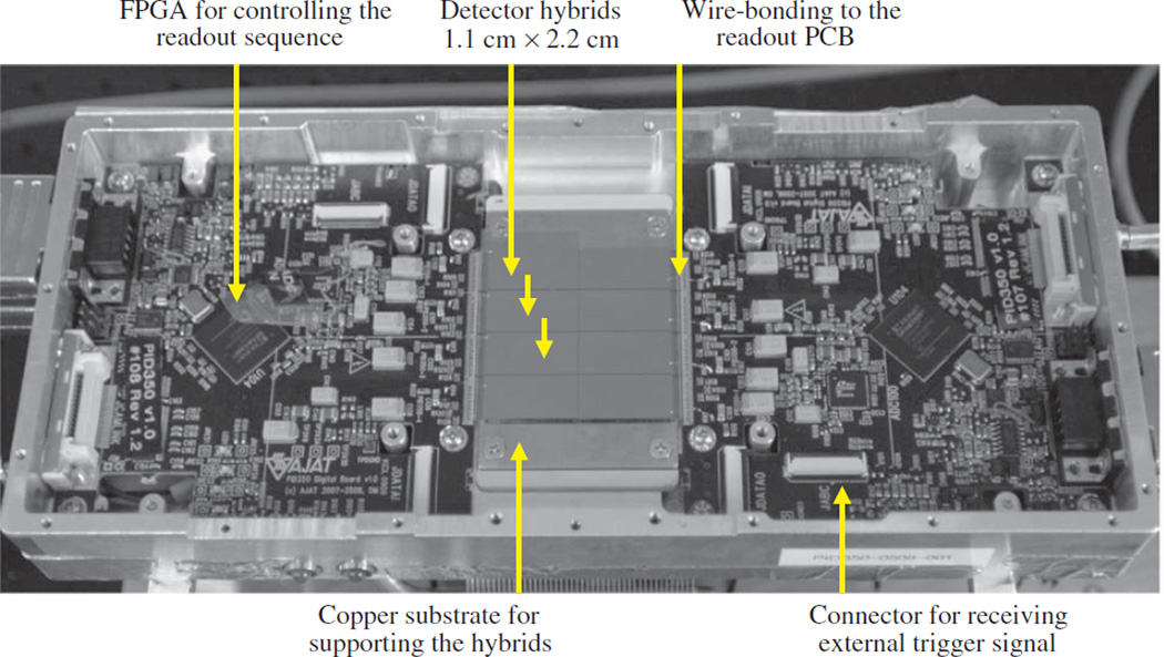
Based on these considerations, the ERPC detector was designed based on the hybrid detector concept. It has a flexible detection area that is made up of multiple closely packed detector hybrids of 1.1 cm × 2.2 cm size. Each hybrid consists of a highly pixelated CdTe (or CZT) crystal, 1–5 mm thick, bump-bonded onto a custom-designed readout ASIC. The hybrids are wire-bonded to readout printed circuit boards (PCBs) that are connected to a host PC though a USB 2.0 interface. A photo of the prototype ERPC detector is shown in Fig. 1. Details of the ERPC detector are discussed in the following sections.
Fig. 1.
The prototype ERPC detector with eight detector hybrids. It offers a detection area of 4.4 × 4.4 cm2.
2.2. Front-end readout circuitry
The ERPC detector consists of multiple CdZnTe or CdTe detectors that are flip–chip bonded onto a newly developed readout ASIC. The ASIC is realized through a mixed signal, 4 metal 2 poly CMOS process based on commercial 350-nm technology. The overall dimensions of the ASIC are approximately 22mm × 11 mm. It accommodates a total of 2048 readout channels arranged in an array of 32 × 64 pixels. The pixel pitch size is 0.35 mm × 0.35 mm, which matches the pixel configuration of CdZnTe or CdTe detectors in use. Each CMOS pixel has a bump-bonding pad of 25 µm diameter. The pixel readout circuitry includes an AC-coupled charge-sensitive amplifier, a peak-hold (P/H) circuit, a comparator and a 10-bit multi-function counter used for both photon counting and A-to-D conversion. The pixel circuitry also contains various logic units for controlling, address decoding and selecting between readout modes. The amplifier has a shaping time of ~1 µs. The comparator in each pixel has a typical differential topology that uses an external analog control voltage to adjust the threshold level. All the wire-bonding pads, including the control signals, power feeds and output signals, are located on one side of the ASIC (as shown in Fig. 1). In order to compensate for the pixel-to-pixel variations in the channel offset and gain, each channel is also equipped with two 8-bit digital-to-analog converters (DACs). These allow accurate alignment of the 16,384 readout channels on the detector.
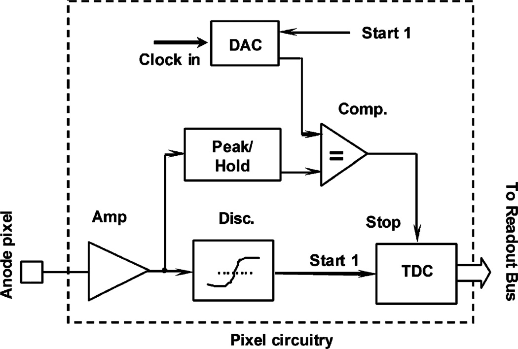
One of the key features of the ERPC ASIC is the capability of on pixel A-to-D conversion with variable precision. Following an interaction in the detector, the trigger signal from an anode pixel is used to initiate a 10-bit time-to-digital converter (TDC) located on the same pixel. At the same time, the triggering signal is also used to start a ramp generator. The ramp generator is implemented using an 8-bit digital-to-analog converter (DAC), which is driven by a clock signal operating at 10 MHz. The ramp generator outputs a steadily increasing ramp signal, which is compared with the signal amplitude held by the on-pixel P/H circuitry. When these two amplitudes are sufficiently close to each other, a trigger signal is generated to stop the TDC. Therefore, the output of the TDC is proportional to the signal amplitude induced on the corresponding anode pixel. Depending on the desired count rate capability, one can choose to digitize the analog signal with 4- to 8-bit precision by changing the step size of the ramp generator. For each event, it takes a maximum of 6.4 µs to perform a 6-bit A-to-D conversion and 25.6 µs for an 8-bit conversion. After the A-to-D conversion, the pixel address and the digital amplitude are sent out, and the ASIC is reset for receiving future incoming events. A schematic of the pixel circuitry is shown in Fig. 2. Using this readout mode, each ASIC is capable of handling 100 k counts per second (cps) with 6-bit ADC precision and 25 k cps with 8-bit precision. Since the eight ASICs on each ERPC detector can be operated independently, the entire ERPC detector (4.4 cm × 4.4 cm in size) is capable of a count rate of 0.8 or 0.2 Mcps, depending on the ADC precision. For high-resolution SPECT imaging, the event rate exposed to gamma ray detectors is generally limited by the use of high-resolution collimation apertures [11,12]. Therefore, the count rate of the ERPC detector should be more than adequate for most high-resolution SPECT applications.
Fig. 2.
Pixel circuitry implemented on the EPRC ASPC.
2.3. Digital readout circuitry
In the current ERPC detector, the hybrids are wire-bonded to two digital readout printed circuit boards, as shown in Fig. 1. These PCBs provide the power feed, logic and timing signals and data pathway for the ASICs. Each readout board also has a 32-MB data buffer for temporarily storing pixel addresses and digital signal amplitudes. The readout operation of the camera is controlled by the FPGAs mounted on digital boards, which act as a bridge between the ERPC ASICs and the control software. For the ERPC detector, a universal threshold is used for all readout channels. The threshold level is controlled by an 8-bit DAC located on the readout board. The selectable threshold level has a resolution corresponding to 0.46 keV. The power consumption of a single ASIC in active mode is around 0.8 W. The maximum power consumption of the entire ERPC detector is around 10 W. The eight ASICs are mounted onto a copper back plate, which is attached to a peltier cooling unit for heat dissipation. The digital PCBs are connected to the host PC either through a USB 2.0 or a CameraLink interface.
2.4. Pixelated CdTe detector
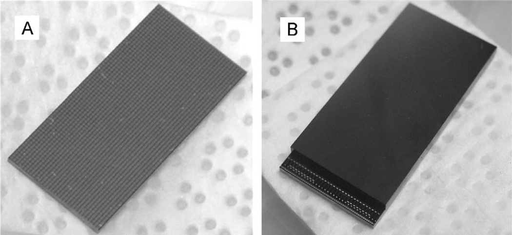
The ERPC detector is designed to readout CdTe or CZT detectors having a thickness of 1–5 mm. In the prototype system, we used high-resistivity p-type CdTe crystals of 1mm thickness (procured from Acrorad). Each detector has a pixel pattern matching that of the readout ASICs, e.g., 32 × 64 pixels with a pitch size of 350 µm. The actual size of the metal contact is 300 µm × 300 µm, with 50 µm gaps between adjacent pixels. No steering grid is implemented between the anode pixels. The 32 × 64 pixel array is surrounded by a guard ring, 25 µm in width, along the boundary of the anode plane. The gap between the guard ring and adjacent anode pixels is 50 µm. A bias voltage of −200 V was applied to the cathodes. The CdTe detectors have ohmic contacts on both the anode and the cathode sides. Photos of a pixelated CdTe detector and a complete detector hybrid are shown in Fig. 3. For gamma rays of 140 keV, the relatively short charge-drifting distance (<1 mm) and the limited range of the photoelectrons or Compton recoil electrons following each gamma interaction lead to charge clouds with relatively small lateral dimensions. With the 300 µm × 300 µm pixels, we expect that most of the electron clouds created by individual gamma ray interactions are collected by single pixels. The probability of single-pixel events should be further increased by reducing the gap to 25 µm in a future CdTe detector (Table 1).
Fig. 3.
(A) The pixelated CdTe detector of 11mm × 22 cm × 1 mm size. The anode side with 32 × 64 pixels is shown in the figure. (B) A CdTe/ASIC hybrid. The cathode side of the CdTe detector is shown on the top, and the ASIC is underneath the CdTe detector, with the wire-bonding pads shown on the lower left side.
Table 1.
Design specifications for the ERPC ASIC.
| Physical dimensions | 1.1 cm × 2.2 cm, with 32 × 64 pixels |
| Pixel size | 350 µm × 350 µm |
| Preamp gain | 10 µV/electron |
| Shaping time | ~1 µs |
| Gain correction | 8-bit |
| Offset correction | 8-bit |
| Threshold control | 10-bit, common to all channels |
| ADC | On pixel, 4-bit to 8-bit |
| Readout modes |
|
| Count rate capability |
|
| Energy resolution (with CZT detector) |
2.5–3.5 keV FWHM@140 keV (measured) |
| Dynamic range | 35–250 keV |
2.5. Preliminary imaging study
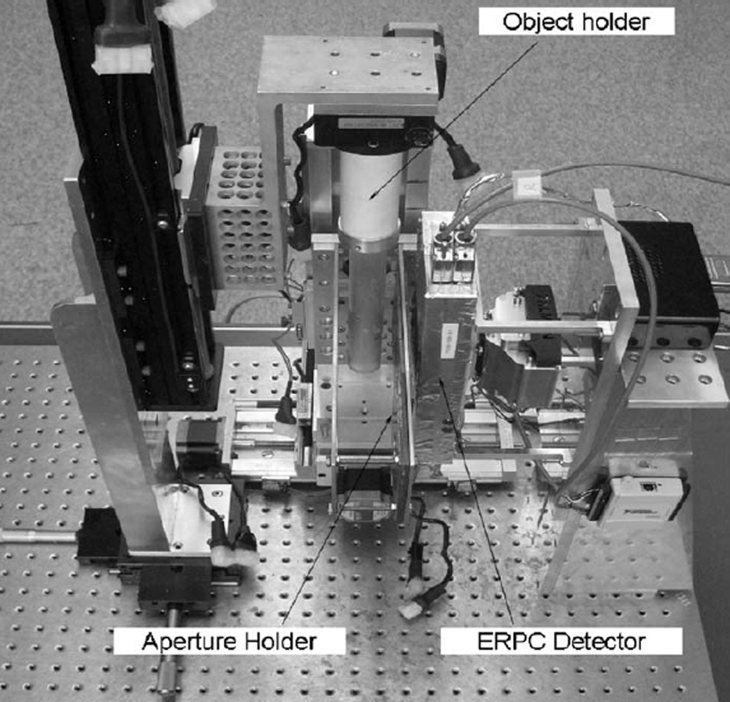
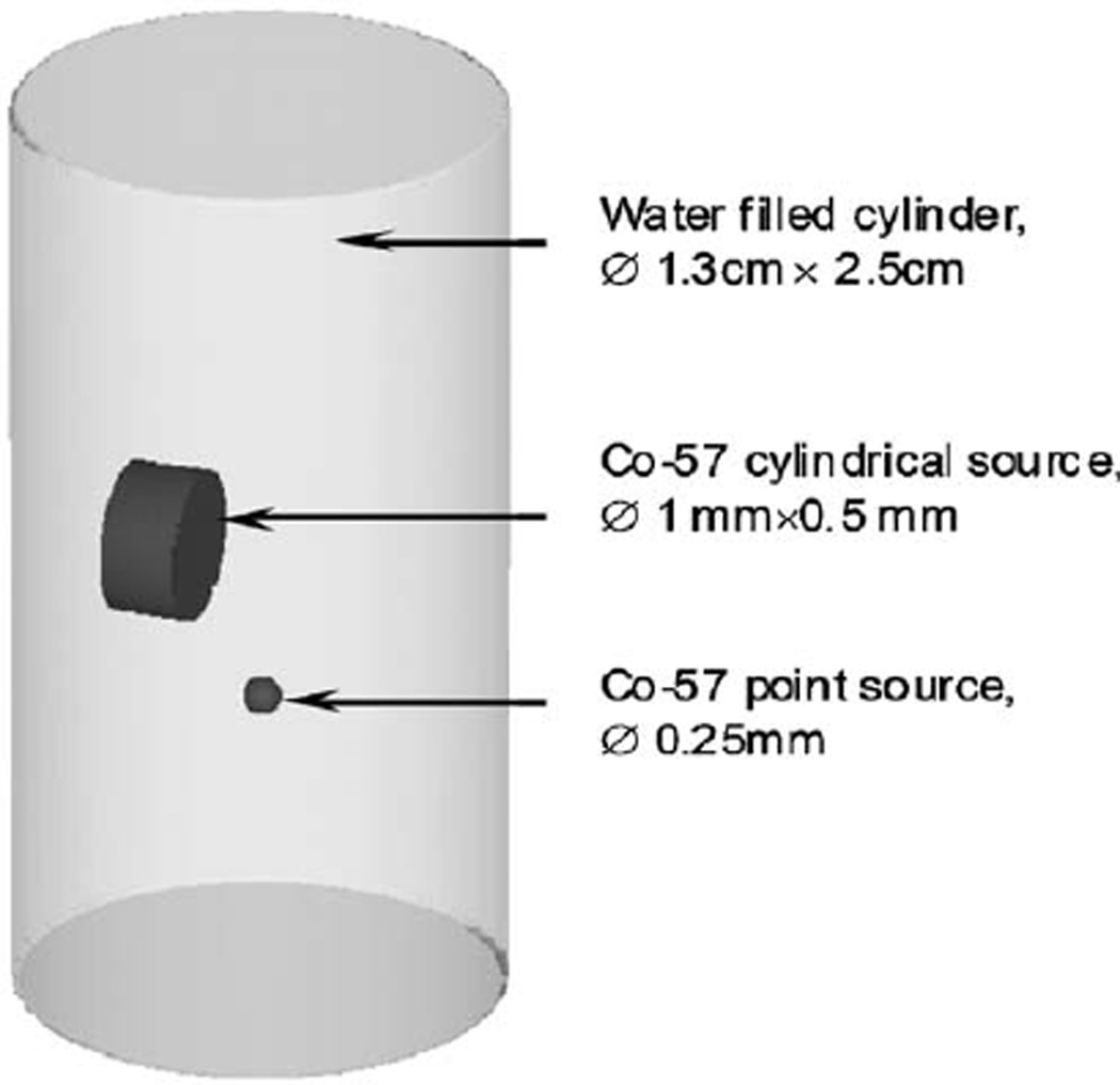
The imaging performance of our ERPC detector was evaluated in a preliminary SPECT study, using the experimental setup shown in Fig. 4. The EPRC detector was fixed on a vertical support. A cylindrical phantom was held on a rotary stage that rotates through 32 angular steps during data acquisition. The phantom consists of a water-filled glass tube, 1.3 cm in diameter. Two Co-57 sources of 100 µCi were inserted in the phantom, as shown in Fig. 5. The collimation aperture was made of a tungsten sheet of 6 mm thickness. It has 5 × 5 pinholes, 200 µm in diameter. These pinholes have sharp knife-edges and acceptance cones of 30° on both sides. The pinhole distance is 4 mm. The detector-to-aperture distance is 2.5cm and the axis of the rotation is 2.5 cm from the central pinhole. In this study, an energy threshold of 110 keV was used to select full-energy events. Image reconstruction was performed using the standard MLEM algorithms with 20 iterations. Photon penetration through pinhole knife-edges was modeled with the analytical equation derived in [21,22].
Fig. 4.
Experimental setup for preliminary imaging study.
Fig. 5.
The resolution phantom used in the preliminary imaging study.
3. Results
3.1. Detector uniformity
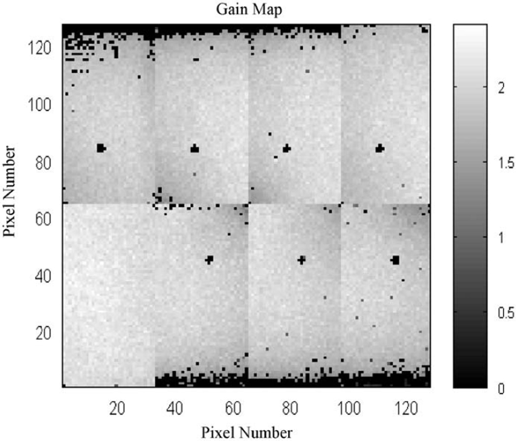
In order to evaluate the performance of the prototype ERPC detector, we used Co-57 and Am-241 point sources of 10 µCi to irradiate the detector from a distance of ~10 cm. From the energy spectrum obtained on each channel, the relative positions of the 59 and 122 keV photopeaks were used to derive the actual gain, offset and energy resolution associated with the given channel. Fig. 6 highlights the observed gain variation over all the readout channels. The gain was given as the number of ADC units per keV of energy deposition. As shown in the figure, there is an appreciable distribution in the gain values. The distribution of gain values is centered at 1.8 ADC-Unit (ADU)/keV and the FWHM of the distribution is approximately 0.5 ADU/keV. In this first prototype ERPC detector, roughly 5% of the pixels did not function properly (shown in the map as pixels with zero gain). This is due to either CMOS defects or bad connections between CdTe pixels and ASICs. Based on the maps of gain and offset over the entire camera, the observed variations can be compensated by tuning the two 8-bit trim DACs implemented on each readout channel. This process was performed with multiple iterations to achieve an optimum alignment between the 16,384 channels on the ERPC detector.
Fig. 6.
Spatial variation in gain across the 16,384 pixels on the prototype ERPC detector. About 4% of the pixels were not functioning. The gain values shown are given in ADC units per keV.
3.2. Measured energy resolution
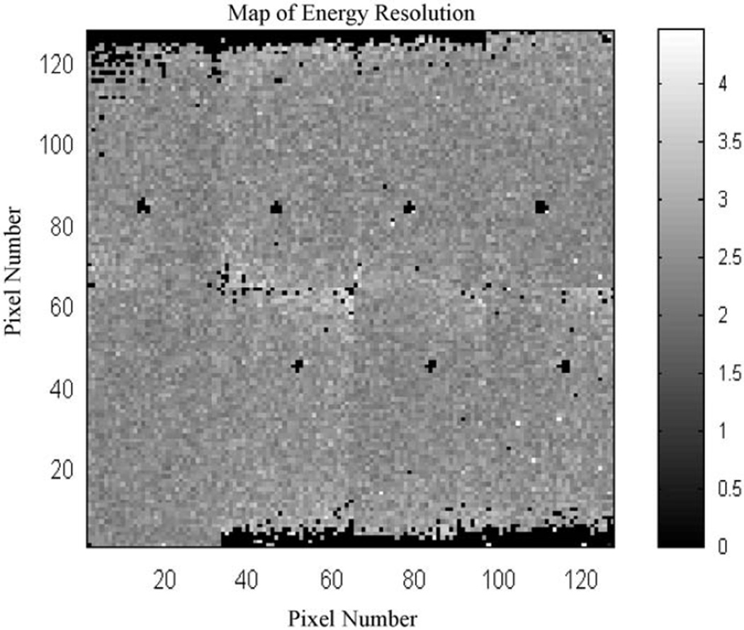
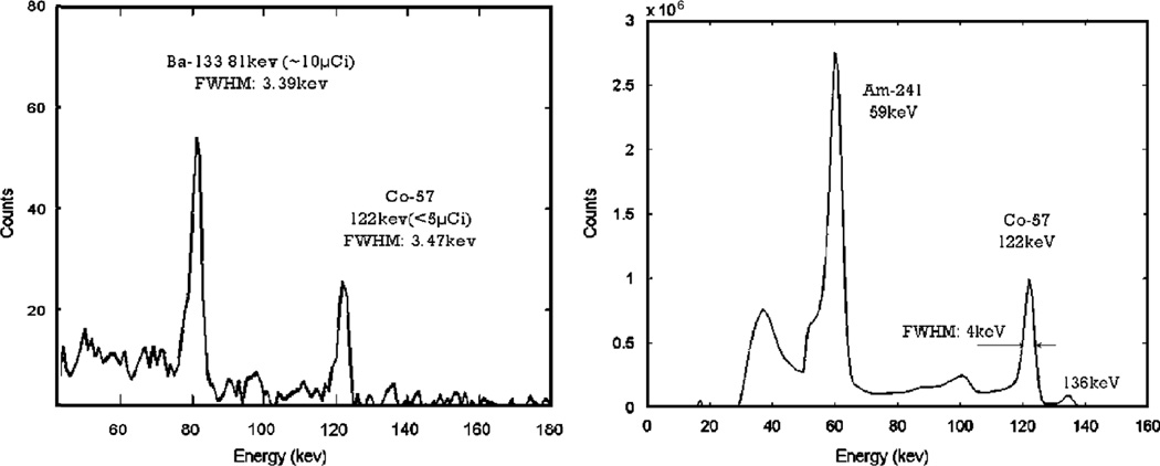
The energy resolutions (FWHM values near the 122 keV photopeaks) measured on all individual channels are shown in Fig. 7. Most readout channels have an energy resolution between 2 and 3.5 keV. Fig. 8 shows a Ba-133 and Co-57 energy spectrum measured on a selected channel, along with a typical energy spectrum that includes all events detected on the entire camera, after careful alignment of all readout channels on the camera. The FWHM of the 122 keV photopeak is ~4 keV, which is slightly worse than the energy resolution achievable on individual channels. This degradation is due to the remaining misalignment between the readout channels. An energy resolution of 4 keV should allow a nice separation between gamma ray lines associated with most radioisotopes commonly used for SPECT imaging applications.
Fig. 7.
Spatial variation of energy resolution (given in keV) across the 16,384 pixels on the prototype ERPC detector. The energy resolution achieved is around 3 keV at 122 keV for most of the pixels.
Fig. 8.
Measured energy spectra on a given pixel (left) and summed over all anode pixels (right).
3.3. Preliminary imaging study
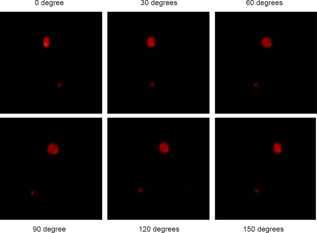
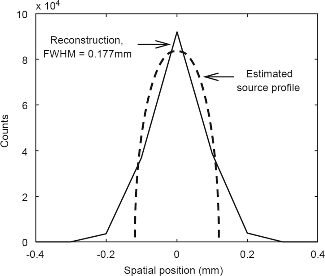
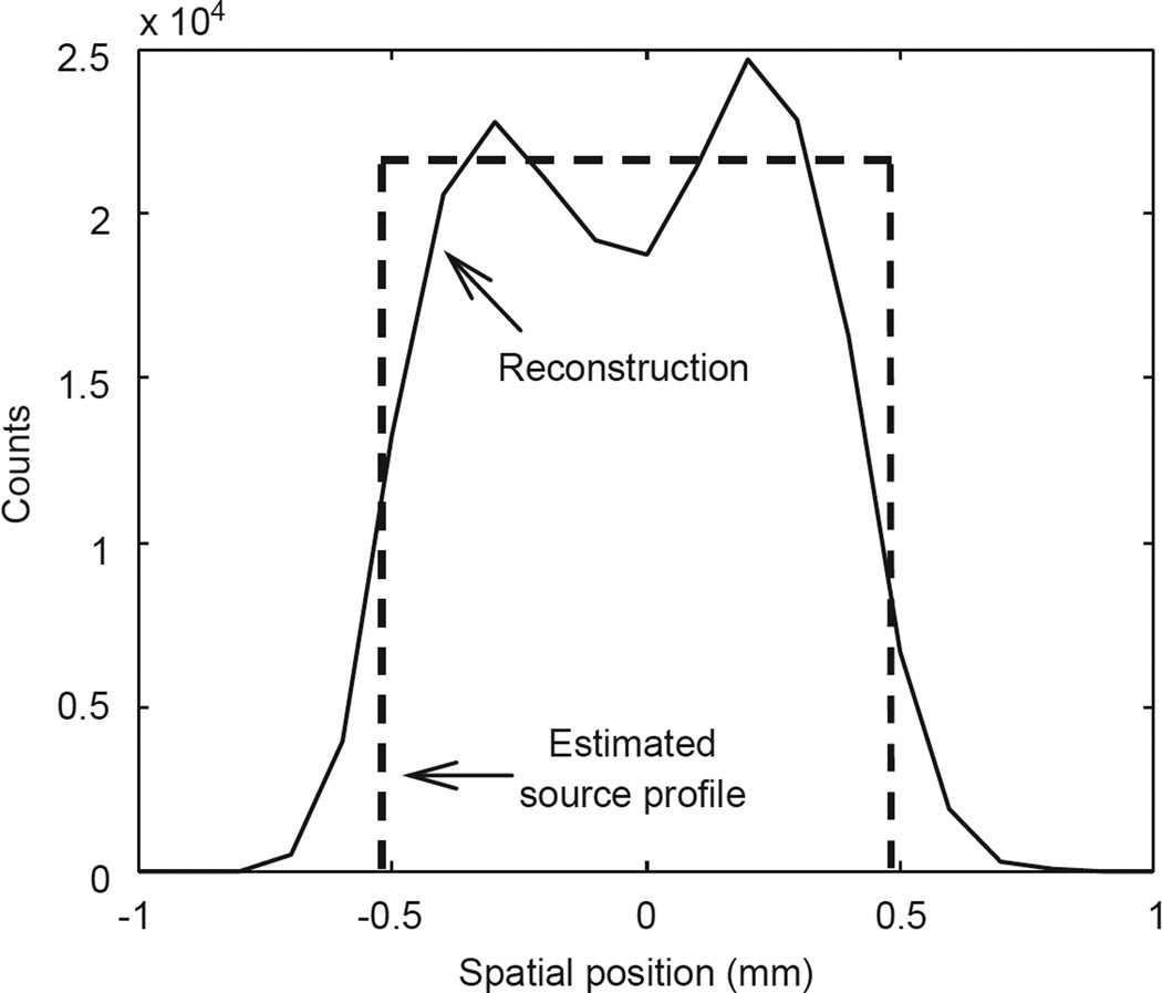
Reconstructed 3D images of the resolution phantom are shown in Fig. 9. The spatial resolution offered by the current experimental setup (with 200 µm pinholes) is demonstrated in the 2D cross-sections of the reconstructed point and cylindrical sources, as shown in Figs. 10 and 11. Since the intrinsic resolution of the system is close to the actual dimension of source objects, it is difficult to obtain the actual point spread function (PSF) directly from the measured data. From the cross-sections shown in Figs. 10 and 11, we estimated that the spatial resolution offered by the prototype SPECT geometry should be less than 250 µm. In this study, the effect of the depth-of-interaction in the CdTe crystals was not modeled.
Fig. 9.
Reconstructed tomographic image of the resolution phantom.
Fig. 10.
1D cross-section of the reconstructed point source image. The source object is a uniform sphere, 250 µm in diameter.
Fig. 11.
1D cross-section of the reconstructed cylindrical source object. The cross-section was taken along a diameter through the center of the cylinder (Ø1 mm × 0.5 mm).
In this initial evaluation, there are approximately 5% of the pixels on the current ERPC detector that have gain values of less than 0.5 ADU/keV. These pixels are mostly distributed around the peripheral as marked in black in Fig. 6. The effect of these pixels on the image reconstruction was minimized by modeling the missing pixels in the system-response function. Given the intrinsic sparseness of SPECT imaging geometry, we expect that a relatively small number of missing pixels should have a negligible impact on the reconstructed image quality. We are currently working on solutions for reducing the number of “bad” pixels in future ERPC detectors.
4. Conclusions and future work
In this paper, we present the design and preliminary performance of a novel energy-resolved photon-counting detector for X-ray and gamma ray imaging applications. This detector is based on a newly developed CMOS ASIC, bump-bonded onto pixelated CdTe detectors. The readout ERPC ASIC has 2048 readout channels arranged in an array of 32 × 64 readout channels with a pitch size of 350µm × 350µm. Each channel is equipped with pre- and shaping-amplifiers, peak-hold circuitry, a discriminator and an ADC. To verify the feasibility of the ERPC detector concept, a prototype detector, consisting of eight CdTe/ASIC hybrids, was developed and experimentally evaluated. It offers a total detection area of 4.4cm × 4.4 cm, an intrinsic imaging resolution of around 350 µm and an energy resolution of 3–4 keV for low-energy gamma rays, which is ideal for simultaneous multiple tracer studies using isotopes such as I-123, Tl-201 and Tc-99 m. It also allows efficient rejection of Compton-scattered gamma rays. The ERPC detector has a compact form factor, with a detection area that can be easily tailored to different applications. These make the ERPC detector well-suited for small animal SPECT applications. The prototype detector was also evaluated in a preliminary SPECT imaging study, using a water-filled phantom that contains Co-57 point and disk sources. The imaging resolution was demonstrated with reconstructed images.
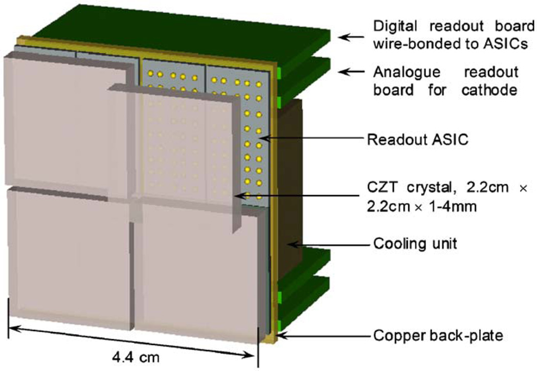
Although the current prototype has exhibited promising imaging and spectroscopic performances, there remain several key aspects that deserve further improvements. Firstly, roughly 5% of the anode pixels were not working properly, presumably due to defects in the CdTe detectors, bad connections through bump-bonding and/or malfunctioning of CMOS readout channels. We are currently exploring the possible causes and potential solutions for this issue. Secondly, despite the compact front end (CdTe/ASIC hybrids), the overall dimensions of the prototype detector are relatively large due to the bulky digital readout board currently in use. Future ERPC detectors will be equipped with readout PCBs, which are much reduced in size and supported at the back of the detectors, as shown in Fig. 12. This offers a modular detector configuration with a minimal dead area at the periphery. Thirdly, as demonstrated by He et al. [23], the depth-of-interaction (DOI) of gamma rays in pixelated CZT detectors can be derived using the ratio between signal amplitudes observed on both the anode and the cathode (C/A ratio). For future ERPC detectors with relatively thick (2–4 mm) crystals, a similar scheme can be implemented to provide 3D position sensitivity at an excellent resolution. This is crucial for reducing the parallax error in SPECT imaging applications. Readout circuitry capable of measuring the C/A ratio is under development.
Fig. 12.
Schematic of the proposed modular ERPC detector.
References
- 1.Brzymialkiewicz CN, Tornai MP, McKinley RL, Bowsher JE. IEEE Tran. Med. Imaging. 2005;24:868. doi: 10.1109/tmi.2005.852501. [DOI] [PMC free article] [PubMed] [Google Scholar]
- 2.Guerin L, Verger L, Rebuffel V, Monnet O. IEEE Trans. Nucl. Sci. 2008;NS-55:1573. [Google Scholar]
- 3.Verger L, Gentet AC, Gerfault L, Guillemaud R, Mestais C, Monnet O, Montemont G, Petroz G, Rostaing JP, Rustique J. IEEE Trans. Nucl. Sci. 2004;NS-51:3111. [Google Scholar]
- 4.Kim H, Furenlid LR, Crawford MJ, Wilson DW, Barber HB, Peterson TE, Hunter WCJ, Liu ZL, Woolfenden JM, Barrett HH. Med. Phys. 2006;33:465. doi: 10.1118/1.2164070. [DOI] [PMC free article] [PubMed] [Google Scholar]
- 5.Singh M, Doty FP, Friesenhahn SJ, Butler JF. IEEE Trans. Nucl. Sci. 1995;NS-42:1139. [Google Scholar]
- 6.Singh M, Mumcuoglu E. IEEE Trans. Nucl. Sci. 1998;NS-45:1158. [Google Scholar]
- 7.Accorsi R, Celentano L, Laccetti P, et al. IEEE Trans. Nucl. Sci. 2008;NS-55(1):481. [Google Scholar]
- 8.Guerin L, Verger L, Rebuffel V, Monnet O. IEEE Nuclear Science Symposium and Medical Imaging Conference Record; 2007. [Google Scholar]
- 9.Spartiotis K, Leppanen A, Pantsar T, et al. Nucl. Instr. and Meth. 2005;550(1–2):267. [Google Scholar]
- 10.Meng LJ. IEEE Trans. Nucl. Sci. 2006;NS-53(4):2376. doi: 10.1109/TNS.2006.878574. [DOI] [PMC free article] [PubMed] [Google Scholar]
- 11.Meng LJ, Clinthorne NH, Skinner S, et al. IEEE Trans. Nucl. Sci. 2006;NS-53(3):1168. doi: 10.1109/TNS.2006.871405. [DOI] [PMC free article] [PubMed] [Google Scholar]
- 12.Meng LJ, Fu G, Roy EJ, Suppe B, Chen CT. Nucl. Instr. and Meth. A. 2009;600:498. doi: 10.1016/j.nima.2008.11.149. [DOI] [PMC free article] [PubMed] [Google Scholar]
- 13.Fu G, Meng LJ, Chen CT. IEEE Nuclear Science Symposium and Medical Imaging Conference Record; 2008. [Google Scholar]
- 14.Beekman FJ, Van Der Have F, Vastenhouw B, Van Der Linden Annemarie JA, Van Rijk PP, Peter J, Burbach, Smidt H, Marten P. IEEE Nuclear Science Symposium and Medical Imaging Conference Record; 2004. [Google Scholar]
- 15.De Vree GA, Van Der Have F, Beekman FJ. IEEE Nuclear Science Symposium and Medical Imaging Conference Record; 2004. [Google Scholar]
- 16.Meng LJ, Li D, Cho SY, Pelizzari C, Souris J, Pan XC, Chen CT. IEEE Nuclear Science Symposium and Medical Imaging Conference Record. 2006 [Google Scholar]
- 17.Chen CMH, Boggs SE, Bolotnikov AE, Cook WR, Harrison FA, Schindler SM. IEEE Trans. Nucl. Sci. 2002;NS-49:270. [Google Scholar]
- 18.Kalemci E, Matteson JL. Nucl. Instr. and Meth. A. 2002;478:527. [Google Scholar]
- 19.Gonzalez R, Perez JM, He Z. Nucl. Instr. and Meth. A. 2004;531:544. [Google Scholar]
- 20.He Z, Li W, Knoll GF, Wehe DK, Berry J, Stahle CM. Nucl. Instr. and Meth. A. 1999;422:173. [Google Scholar]
- 21.Metzler SD, Bowsher JE, Greer KL, Jaszczak RJ. IEEE Trans. Med. Imaging. 2002;21:878. doi: 10.1109/tmi.2002.803129. [DOI] [PubMed] [Google Scholar]
- 22.Cao ZX, Bal G, Accorsi R, Acton PD. Phys. Med. Biol. 2005;50:4609. doi: 10.1088/0031-9155/50/19/013. [DOI] [PubMed] [Google Scholar]
- 23.He Z, Li W, Knoll GF, Wehe DK, Berry JE, Stahle CM. 3-D position sensitive CdZnTe gamma-ray spectrometers, Nuclear Instr. and Meth. A. 1999;422:173. [Google Scholar]


