Abstract
This paper presents experimental results on the timing resolution achieved with a 5 mm thick HgI2 detector. The timing information was derived based on the cathode pre-amplifier pulse waveform, measured using a digital oscilloscope. The times of interaction were estimated by fitting the measured pulse waveforms to pre-defined waveform models. With this approach, problems related to the conventional leading edge or constant fraction triggering, such as slow charge carrier mobility, pulse shape variation and depth-dependent detector response can be greatly reduced. As a result, we showed a 13 ns timing resolution measured using the 5 mm thick HgI2 detector and a BaF2 coincidence detector with 511 keV full energy events. In this paper, we discuss several waveform models and the results achieved using these models.
Keywords: Large volume HgI2 detector, Timing resolution, Pulse waveform
1. Introduction
Mercury iodide is a semiconductor material that possesses several attractive properties for detecting hard X-rays, gamma rays and other particles. It has a wide band-gap (2.13 eV) allowing room temperature operation. It also has a high density (6.4 g/ml) and a high effective atomic number, which result in a high stopping power and a high photo-fraction. However, there are some intrinsic difficulties for using HgI2 as the detector material. These include low charge carrier mobility, significant charge trapping, polarization, material non-uniformity and surface degradation. Extensive efforts have been made to adapt HgI2 for X-ray and gamma-ray detection applications [1,2]. Baciak and He reported the results of using large-volume HgI2 detectors for gamma-ray spectroscopy. Good energy resolution (<2%) was achieved using a 1 × 1 × 1 cm3 HgI2 detector after correction for the charge trapping effect [3,4]. In principle, one can apply the 3-D position sensitive readout scheme, formerly developed for CZT sensors, to the large volume HgI2 detectors. This would lead to a detector with a high sensitivity, high energy resolution and high spatial resolution.
The focus of this work is to explore the timing resolution achievable on thick HgI2 detectors. In order to overcome the difficulties in conventional analog triggering methods, we used an alternative approach that extracts interaction times from measured cathode pulse waveforms. Some theoretical considerations and experimental results are presented.
2. Materials and methods
2.1. Waveform analysis for extracting timing information
Interaction timing information is crucial for many imaging applications, including Compton camera and Positron Emission Tomography (PET). One of the most common ways to obtain timing information is to trigger on amplified signals. This scheme is, however, less feasible for large volume HgI2 detectors. The low mobility of charge carriers limits the achievable signal-to-noise ratio (SNR) on the shaping amplifier output. It is difficult to achieve a good timing resolution by triggering on such signals. Furthermore, interactions that occur at different depths, between the anode and the cathode, would induce pulses with different peaking times. For HgI2 detectors of 1 cm thickness, this effect causes significant time walk, which is difficult to compensate.
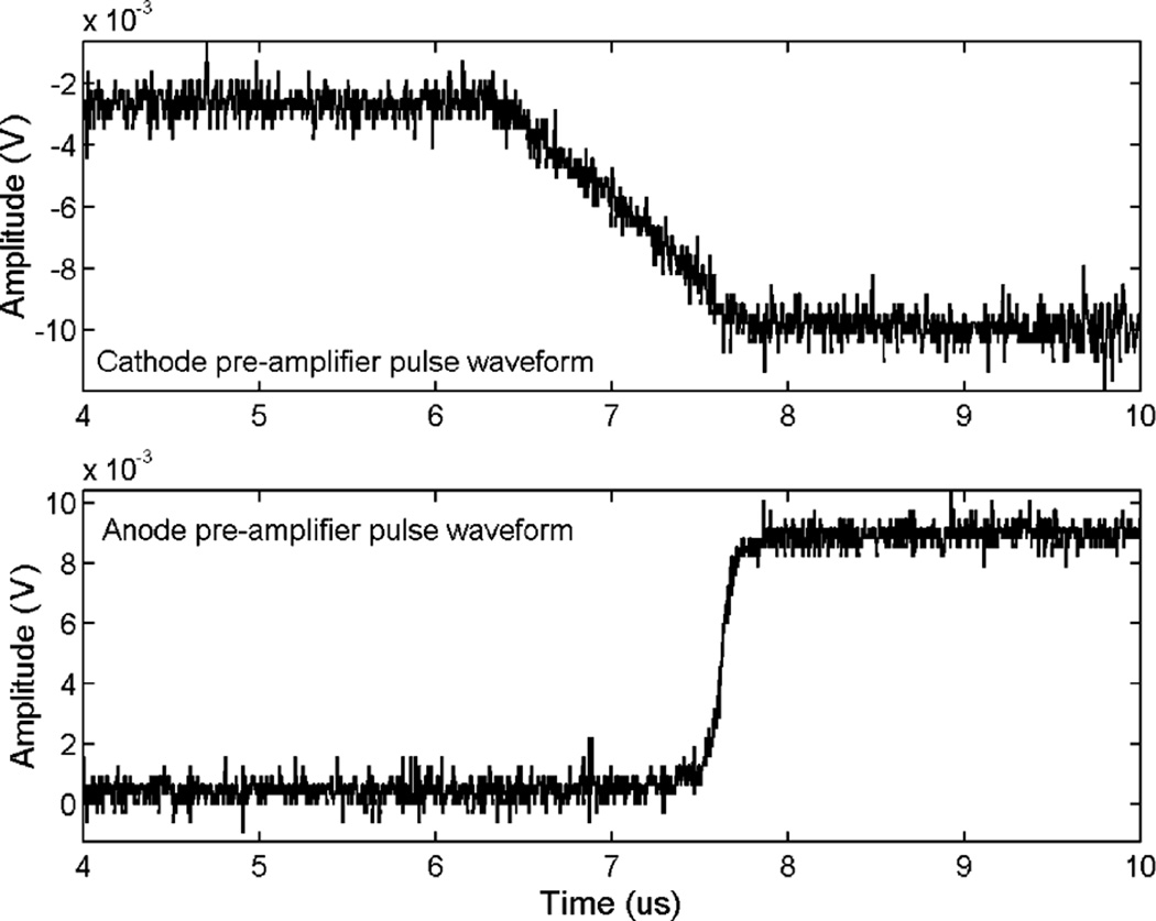
To overcome these difficulties, we explored an alternative approach that utilizes the cathode pulse waveform to estimate the interaction time directly. The idea is to fit the measured pulse waveform to pre-defined waveform models, which is characterized by several parameters including interaction timing. We tested this approach with a 10 × 10 × 5 mm3 HgI2 detector. Detailed operating characteristics of this detector can be found in [3]. It has four anode pixels of 1 × 1 mm2, surrounded by a large non-collecting anode. In this detector, the depth of interaction can be estimated using the ratio of cathode to anode signal amplitudes, which we refer to as CAR in the following text. The induced charge on these anode pixels and the planar cathode are read out individually using discrete pre-amplifiers (Amptek A250 [5]). An HP digital oscilloscope is used to digitize the preamplifier output. It is capable of sampling at 4GHz with 8 bit precision. An example of the measured pulse waveforms is shown in Fig. 1. Note that the relatively small pixel size results in the so-called small pixel effect [6]. When the drifting electron cloud is relatively far from the pixel surface, it induces only a very small signal on the anode readout circuitry. As the carriers approach the vicinity of the anode pixel, the induced charge rises rapidly to its maximum. This sharp rising edge will be used to indicate a full collection of the free electrons. Some common characteristics of the cathode waveforms are given in Table 1. The ratio between the slope of the cathode falling edge and the cathode readout noise level sets an intrinsic limit on the achievable timing resolution using this approach.
Fig. 1.
Measured cathode and anode pre-amplifier output waveforms for a detected event with 511 keV energy deposition.
Table 1.
Typical characteristics of the pulse waveform
| Characteristics | |
|---|---|
| Typical cathode pulse height | ~8 mV per 511 keV |
| Electron drifting time | 0–1.8 μs |
| Cathode pre-amp output noise RMS | 0.24 mV |
| Anode pre-amp output noise RMS | 0.36 mV |
| Cathode falling-edge slope | ~4 mV/μs |
2.2. Pulse waveform models and timing estimation
As far as the cathode pulse waveform is concerned, the HgI2 detector used can be approximated as having a planar geometry, in which the lateral dimension (covered by readout electrode) is much larger than its thickness. We can assume that the internal electric field is uniform across the volume of interest. The pulse waveform expected from such a detector is given by the Hecht relation [7]. If we include the charge trapping effect only and ignore the possible de-trapping effect, the induced charge on a planar electrode as a function of time t for carriers of a single polarity is given by
| (1) |
where TC is the time by which all free charge carriers are collected. N0 is the number of charge carriers initially generated and τf is the mean-free time of the carriers.
Given that the measured waveforms can be assumed to follow multivariate Gaussian distributions, a straightforward approach would be fitting the measured pulse waveform to the Hecht relation using the weighted least-squares (WLS) method that estimates model parameters by minimizing the following object function:
| (2) |
where Q is a vector containing the measured waveform and Q̄ is the mean of the waveform. KQ is the covariance of the measured waveform, which quantifies not only the uncertainty of the pulse amplitudes at given sampling times, but also the correlation between samples acquired at different times. We used a Matlab code that implements the Levenberg–Marquardt method [9] for the fitting. Suppose that the number of parameters is n and the number of data points in each waveform is m; one iteration of the least-square fitting process requires ~2nm floating point operations. If ten iterations are used in the fitting, we need ~2 × 10nm floating point operations for each timing estimation. For n = 5 and m = 500, one would need ~12.5 μs for each event, using a processor capable of 4G floating point operations.
In order to reduce the amount of computation required, we also tested simpler models that include fewer parameters. These models are outlined in Table 2. The Double Exponential model consists of a linear section joining a waveform section given by the Hecht relation. The Linear mode simply assumes that the cathode waveform has a linear rising/falling edge corresponding to the initial electron drifting period.
Table 2.
Waveform models used in timing estimation
| Waveform models | Definition | No. of model parameters | |
|---|---|---|---|
| Double exponential | 7 (λ1, λ2, t0, λ3, λ4, λ5 and λ6) | ||
| Single exponential | 5 (λ1, λ2, t0, λ3 and λ4) | ||
| Linear | 4 (λ1, λ2, t0 and λ3) |
2.3. Uncertainty of the measured waveforms
To use WLS estimation, we need to know the uncertainty associated with the measured waveforms, e.g. the covariance of the data (matrix KQ in (2)): This uncertainty consists of several components, including factors such as readout electronic noise, statistical fluctuation due to charge generation and transportation. We assumed that the readout electronics contributes a Gaussian white noise with known root-mean-squares (RMS). The following discussion will be focused on evaluating the statistical contribution from carrier generation and transportation inside the detector. Measured pulse waveforms are the results of many independent random drifting processes by a large number of carriers, initially generated by incident gamma rays. Given an energy deposition, the number of electron–hole pairs may be approximated by a Gaussian distribution with its variance given as [7]
| (3) |
where F is the Fano factor for HgI2. Eγ and W are the energy deposition and the mean energy required for generating an electron–hole pair.
We assumed that all carriers generated at a depth z inside the detector are travelling at a constant velocity unless trapped in the material. We further assumed that the trapping centers are very sparsely distributed in the bulk. For each trapping center, it has a very small probability of being occupied. Therefore, the number of free carriers as a function of t follows an exponential law. At a given time t < TC (assuming the interaction occurred at t = 0), the instantaneous spatial locations of those carriers are distributed randomly with a density function given as the following:
| (4) |
where rect[u] = 1, if |u| ≤ 1/2 and 0 otherwise. This particular form is due to Barrett [6].
For the following derivation, we ignored the effect of carrier diffusion and assumed no spreading in lateral dimensions. All charge carriers are distributed on a straight line along the z direction (perpendicular to both anode and cathode planes). The mean of the instantaneous induced signal on the cathode as a result of the movement of electrons is
| (5) |
with ϕ(z) the weighting potential function in 1-D [8]. The random distribution of the charge carriers results in an uncertainty on the instantaneous induced charge. At a given time t, the variance of the induced charge on the cathode by moving charge carriers, including both electron and holes, is given as [6]
| (6) |
The covariance of the waveform can be similarly derived as
| (7) |
where τe and τh are the mean free times of electrons and holes in HgI2. Ae(u) and Ah(u) are the mean weighting potential changes induced by movements of a single charge carrier within a period u,
| (8) |
and
| (9) |
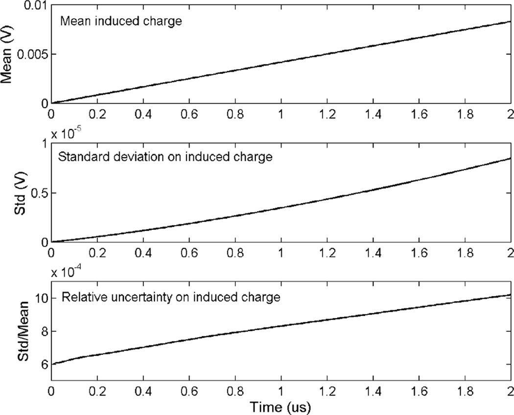
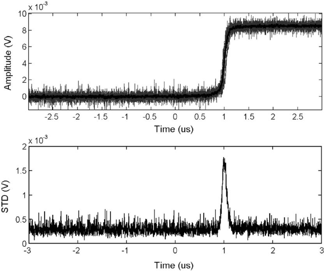
with p(z, t|t0, z0) the pdf for the 1-D distribution of the charge carrier at time t, defined in (4). Because of the uniform internal field, A(u) is a function of drifting time u only. Detailed derivation of the covariance of the waveform is given in Appendix I. Fig. 2 shows the calculated mean, standard deviation of cathode pulse waveforms from a 0.5 cm thick HgI2 detector, as a result of the 511 keV energy deposited near the cathode. In this case, we used a Fano factor of 0.1 [9] for HgI2. The estimated values of μe and τe were ~60 cm2/Vs and ~100 μs respectively, taken from our previous measurements.
Fig. 2.
Calculated mean, standard deviation of a typical cathode pulse waveform.
Note that according to this simple charge transport model, the statistical fluctuation on the waveform is very small. For a 511 keV energy deposition in HgI2, after a 2 μs drifting time, the statistical fluctuation on the instantaneous induced charge would be ~0.1%. It increases to ~0.2% after a 5 μm drifting period. For the energy range that we are interested in (>200 keV), the overall fluctuation on measured pulse waveforms is dominated by the Gaussian white noise introduced by the readout electronics. The overall covariance matrix can be approximated as a diagonal matrix
| (10) |
3. Results
3.1. Digital shaping and triggering approach
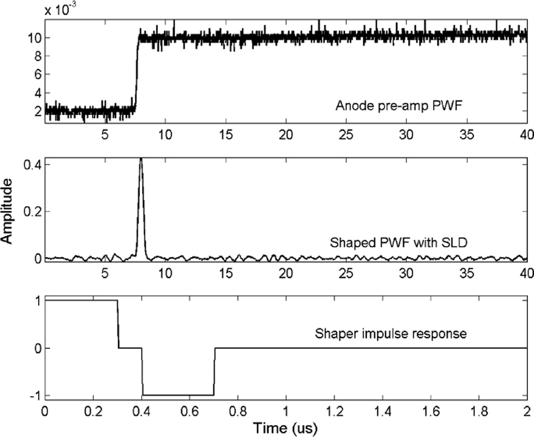
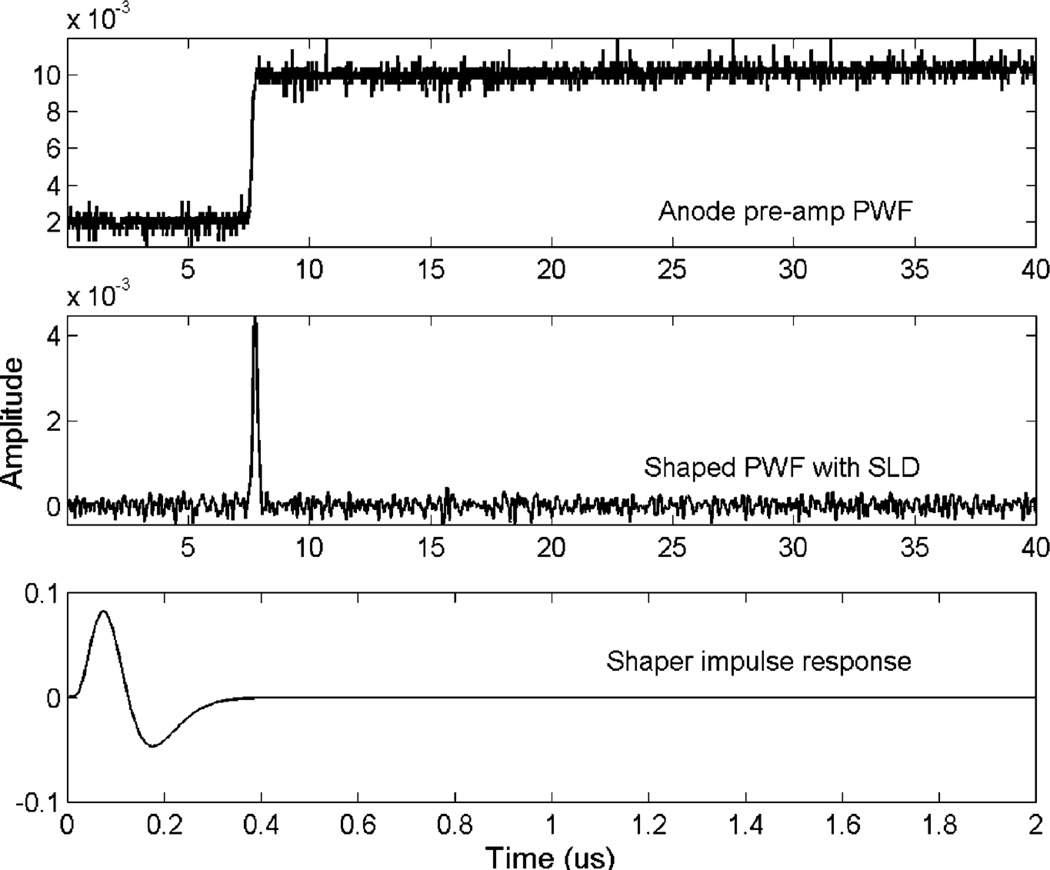
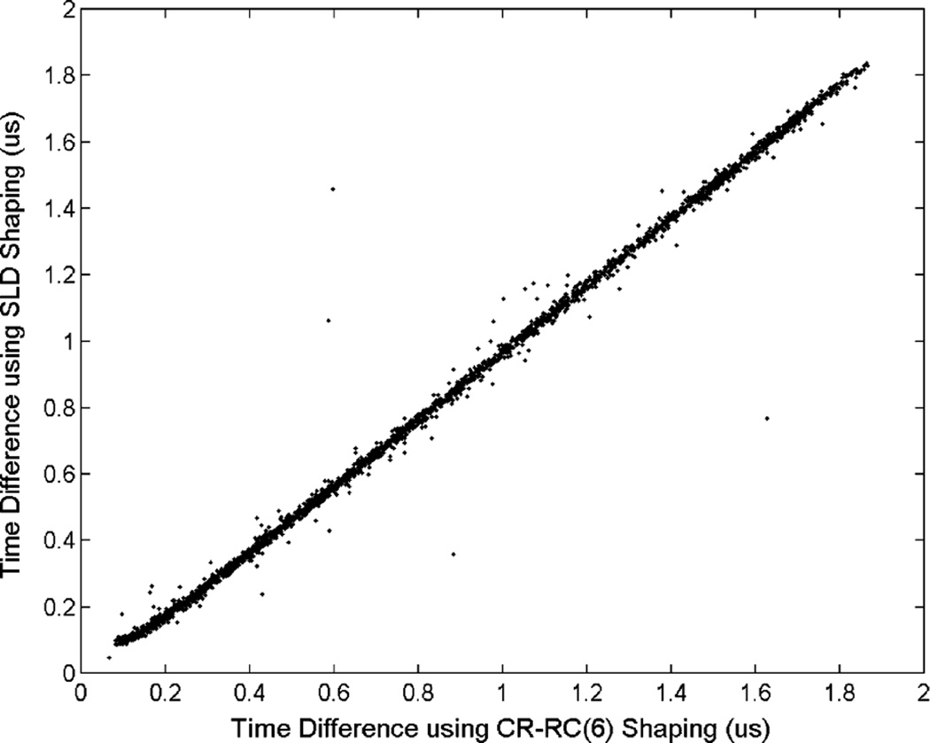
The first approach that we used for finding the timing information is digital shaping and triggering. The sharp rise of the anode signal (as shown in Fig. 1, lower panel) provides a time by which free electrons are fully collected. If the electron drifting time is fixed for all interactions occurring at the same depth and its value is known, one may estimate the interaction time by this triggering time minus the mean electron drifting time. To test this approach, we applied two digital shaping functions to the anode pre-amplifier signal. The first one was a digital CR–RC(6) shaper with a 125 ns shaping time. The second digital shaper used a sliding linear differential (SLD) shaper function. An example of shaped signals using these shapers and the responses of these shaper functions to a δ-impulse are shown in Figs. 3 and 4. After shaping, we applied a digital constant fraction (CF) triggering to the outputs of both shapers to provide timing signals. The resulting timing differences between the triggering times and the actual interaction times given by the BaF2 coincidence detector are compared in a scatter plot in Fig. 5. Both shaping methods gave very consistent timing information with similar estimation errors.
Fig. 3.
Pre-amplifier output pulse waveform and shaped pulse using the SLD shaping function. Top panel: measured pulse waveform; middle panel: signal after shaping; bottom panel: the SLD shaper response function, which is the output of the digital shaper for a delta input function in time domain.
Fig. 4.
Pre-amplifier output pulse waveform and shaped pulse using the CR–RC(6) shaping function. Top: measured pulse waveform; middle: signal after shaping; bottom: the CR–RC(6) shaper response function, which is the output of the digital shaper for a delta input function in time domain.
Fig. 5.
Comparing timing results using CR–RC and SLD shaping functions. The “Timing Difference” refers to the difference between triggering times from shaping/CFD approach and the BaF2 coincidence detector.
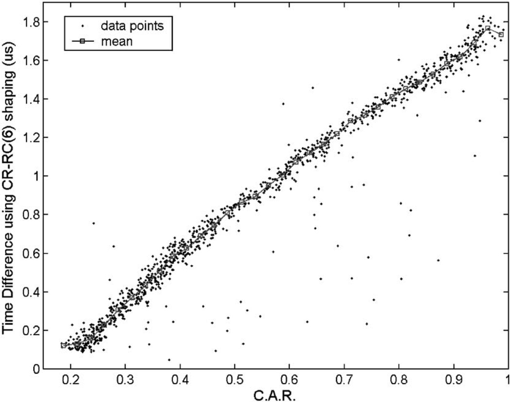
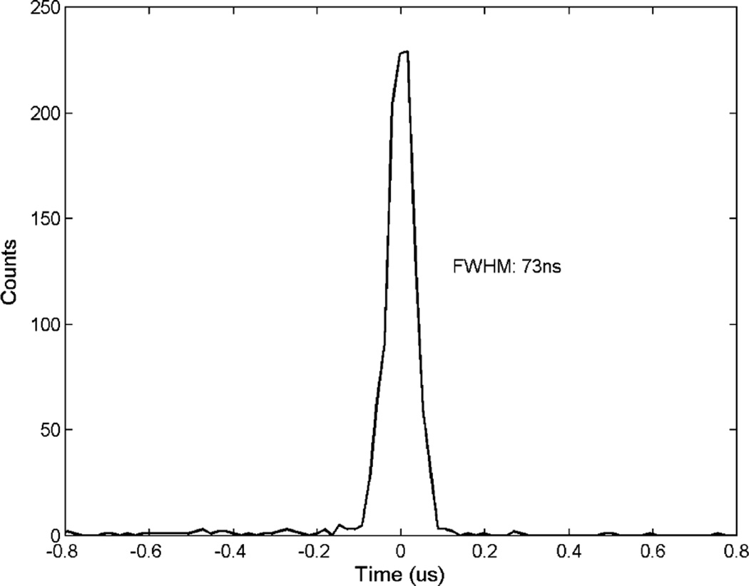
The depth dependence of electron drifting time is shown in Fig. 6. To estimate the mean electron drifting time as a function of interaction depth, we divided all data points into 24 bins, each corresponding to a small range of CAR (or depth). The centroids of points in each bin were derived and used as the mean drifting time for all events in this group (also shown in Fig. 6). The interaction time is then given by the time of triggering minus the mean drifting time. This resulted in a timing spectrum as shown in Fig. 7. The FWHM timing resolution was a disappointing 73 ns, despite the very fast rising edge of the anode signal.
Fig. 6.
Difference between triggering times from CR–RC/CFD and the BaF2 coincidence detector, as a function of CAR (or interaction depth).
Fig. 7.
Timing spectrum achieved with the CR–RC/CDF approach.
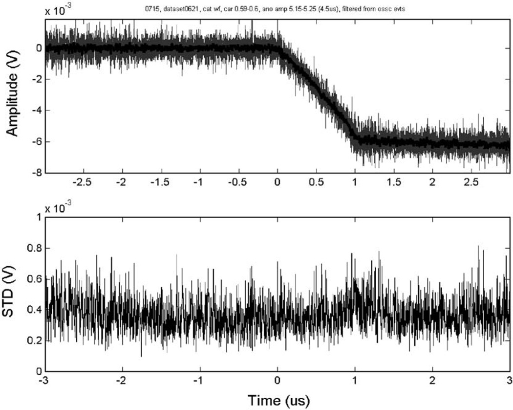
A closer examination on this result revealed that although the digital shaping and triggering based on the sharp anode rising edge gives a prompt signal when all electrons are collected, there is, however, a significant fluctuation on the electron drifting/collection time even for events occurring at the same depth and with the same energy deposition. This may be due to the distortion of electric field near the readout anode. When an electron cloud comes close to the anode, it may take one of many possible routes towards the anode and finally get collected. This effect introduces an uncertainty in the final collection time and ruins the overall accuracy for estimating the interaction time. This effect is shown in Figs. 8 and 9, in which we superimposed 20 measured cathode and anode waveforms and their averages. All pulses are chosen to have almost identical amplitudes and interaction depths. In these figures, all waveforms are lined up for the same interaction time based on the timing information from the BaF2 detector. It is easily seen that within the final electron collection period, there is a significant non-uniformity in the anode pulse waveforms. This effect limits the accuracy of this approach.
Fig. 8.
Uniformity of cathode waveforms. The upper panel shows 20 waveforms, with almost identical amplitudes and CARs. These waveforms are aligned to the same starting time based on the timing information from the BaF2 detector. The lower panel shows the standard deviation of the amplitudes of all waveforms at given times.
Fig. 9.
Uniformity of anode waveforms. The upper and lower panel shows similar information as described in Fig. 7. Note that the anode waveform varied significantly during the final electron collection period. This is evident in the lower panel that showed much increased fluctuations amongst the 20 waveforms.
Although this approach is not sufficiently accurate, it provides some useful information for further refining the timing estimation. Firstly, it provides a relatively accurate timing (Tc) by which free electrons are fully collected. This information is used later in timing estimations with the model fitting approaches. Secondly, as this approach can be implemented with simple hardwares, it provides an easy way for a first-order selection of possible coincidence events. More complicated and time consuming estimation schemes can then be applied only to those selected events and therefore the overall amount of computations can be reduced.
3.2. Comparing linear and exponential waveform models
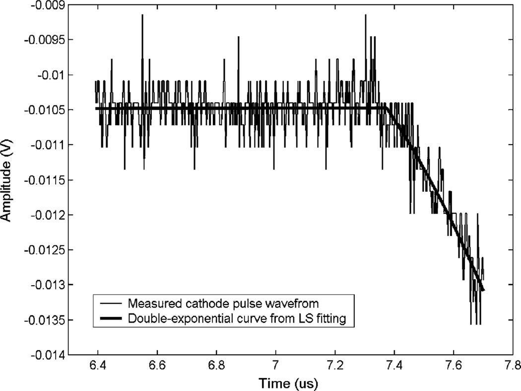
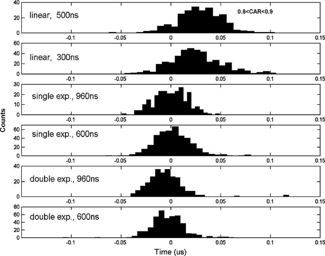
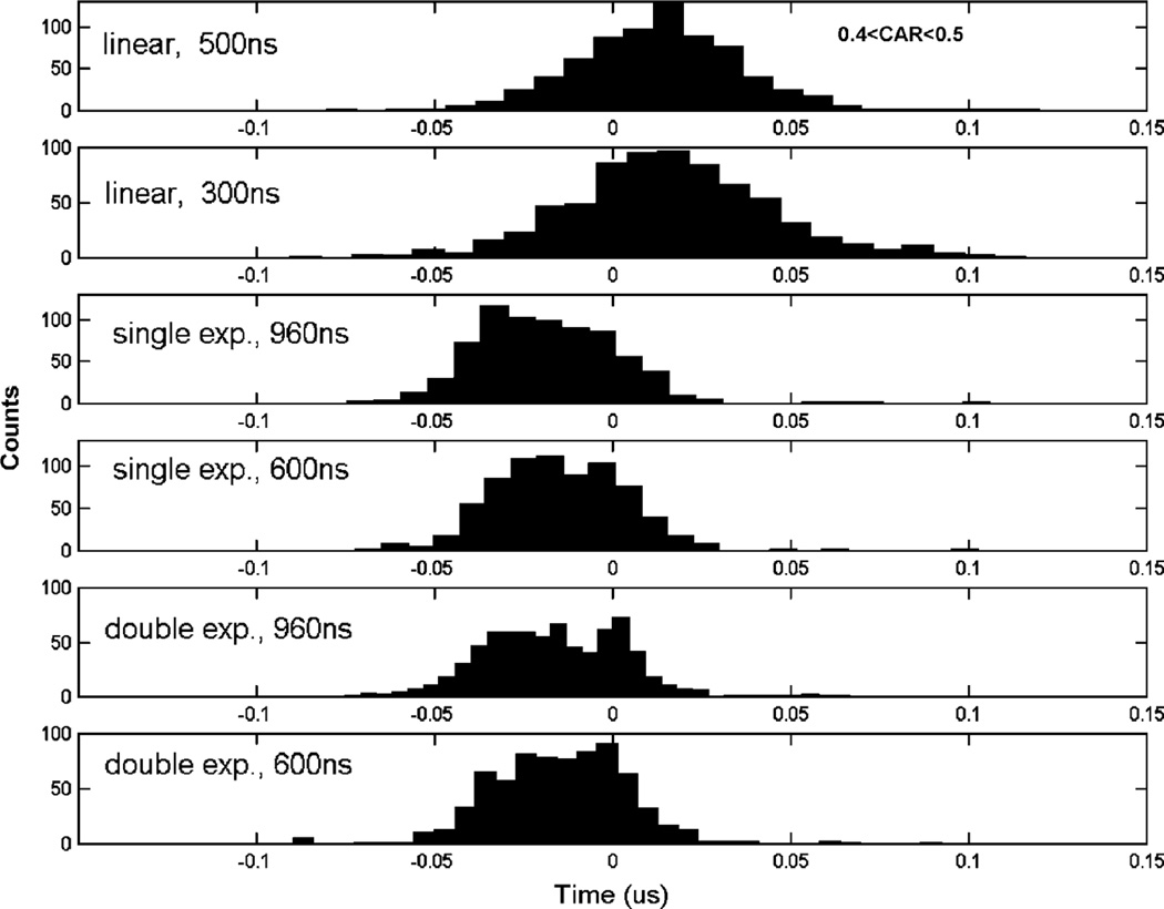
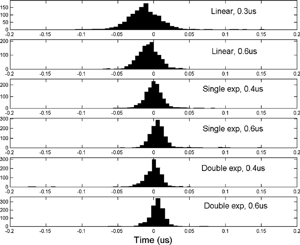
A second approach that we tested is fitting the cathode waveforms to models outlined in Table 2. For this, 1 million coincidence events were recorded. Each waveform consists of 2000 samples with 5 ns intervals. We selected events having 511 keV full energy depositions and CARs falling in the range of 0.4–0.5 and 0.8–0.9. These correspond to full energy events that occur either near the cathode or midway between the anode and cathode. For the actual fitting, we did not use the entire waveform. Instead, we used a section of the waveform that contains a certain length on the falling edge of the cathode waveform, ranging from 300 to 1000 ns. This is based on the electron collection time derived using the digital shaping and triggering approach described in the last section. An example of the fitting process is shown in Fig. 10. The spreading of the estimated interaction times using different models and different lengths on the waveform falling edge are shown in Figs. 11 and 12. These results revealed that the use of the single or double exponential model produced much better timing accuracy. This is presumably because these more complicated models better describe the waveforms and allow more degrees of freedom in the fitting. They can account for the curvatures in the waveform better than the linear mode. In principle, including a longer electron drifting period in the fitting process would improve the statistical accuracy. However, when the model used does not fully represent the actual waveform, including more data points on the falling edge sometimes introduces systematic error in the fitting and degrades the estimation accuracy. For the datasets that we used, the double exponential model with a maximum of 600 ns drifting period produced the best overall timing resolution.
Fig. 10.
An example of the fitted double exponential curve (black) using the WLS method. The measured cathode waveform (blue) is corresponding to a 511 keV energy deposition with a CAR ≈ 0.5.
Fig. 11.
Timing spectra by fitting measured data to different waveform models. Only those events that occurred close to the cathode were included. Both waveform models used and the lengths of electron drifting period included in data are shown in the figure.
Fig. 12.
Timing spectra by fitting measured data to different waveform models, using events that occurred in the middle (along the z direction) of the detector.
3.3. Correction for depth dependence
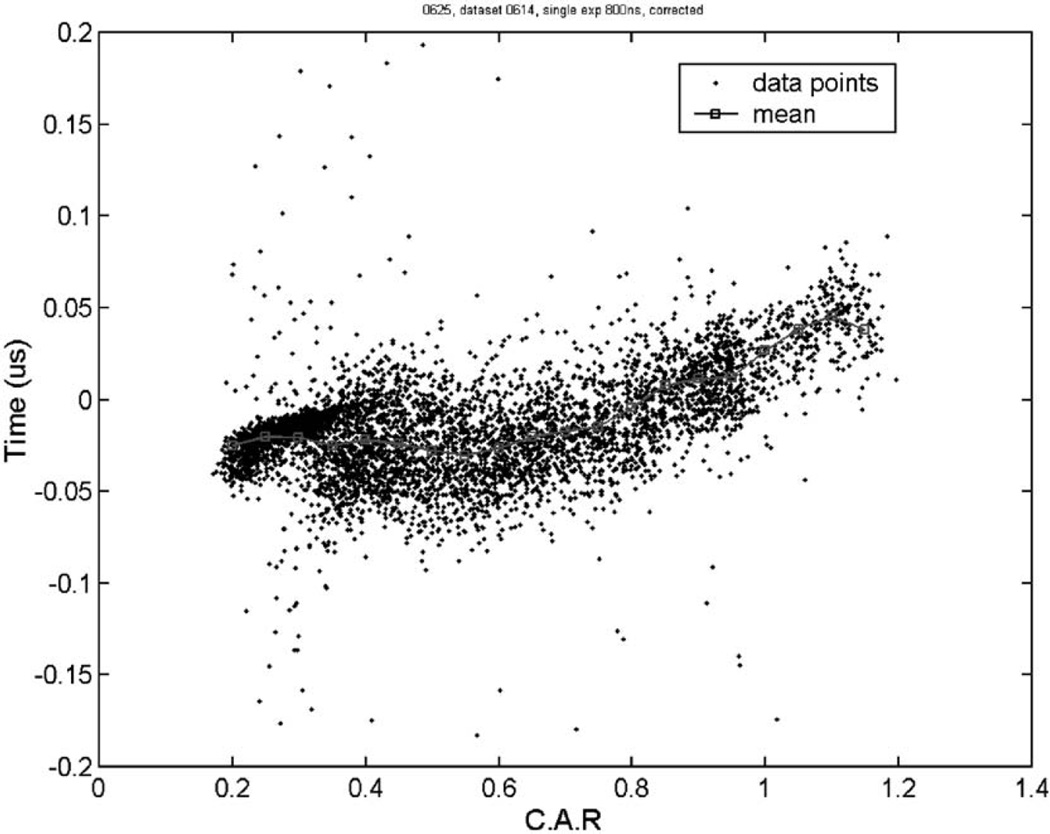
In practice, the actual waveform may deviate from the simple models that we applied. In this case, the fitting process will generate systematic error in the timing estimation. One example is shown in Fig. 13. We applied the double exponential model to all detected events inside the detector active volume. The waveforms used were truncated so that they contained a maximum of 600 ns on the falling edge. For those interactions that occurred near the anode, the electrons will drift for a period shorter than 600 ns. So the actual section of the cathode waveform falling edge ends at Tc-50 ns. From the distribution of estimated interaction times, we see that the estimated interaction times are systematically biased from the true interaction times given by the BaF2 detector. The magnitude of this bias depends on the depths of interaction.
Fig. 13.
Distribution of estimated interaction time. The actual interaction time is normalized to zero based on the BaF2 timing signal.
One possible cause of this depth dependency is the electric field non-uniformity within the active volume. For this particular detector configuration, we see experimentally that there exists a field gradient in the detector active volume. The field strength is stronger in volume closer to the readout anode pixel and reduces gradually when moving towards the cathode. This field configuration tends to make the falling edge of the actual cathode waveform bend downwards from that predicted by Hecht’s relation. Since this effect is interaction-depth dependent, the resulting systematic error in timing estimations will also vary according to the corresponding interaction depths. In addition, for interactions that occur at different depths, we used different numbers of data points on the fall edge in the fitting. This may also introduce some systematic error in timing estimation.
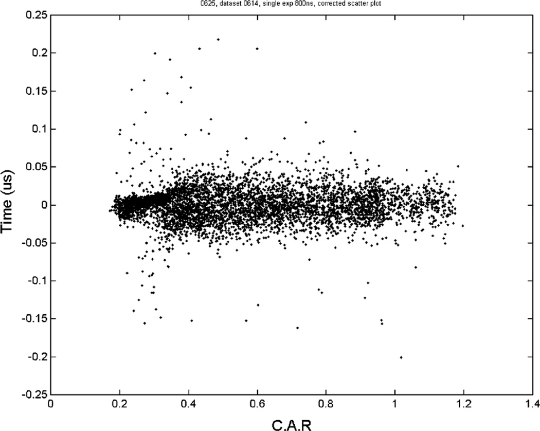
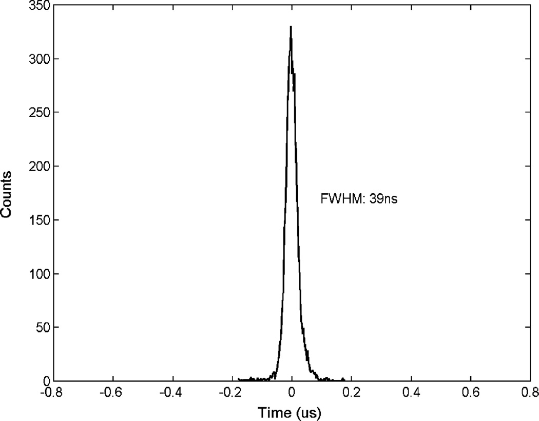
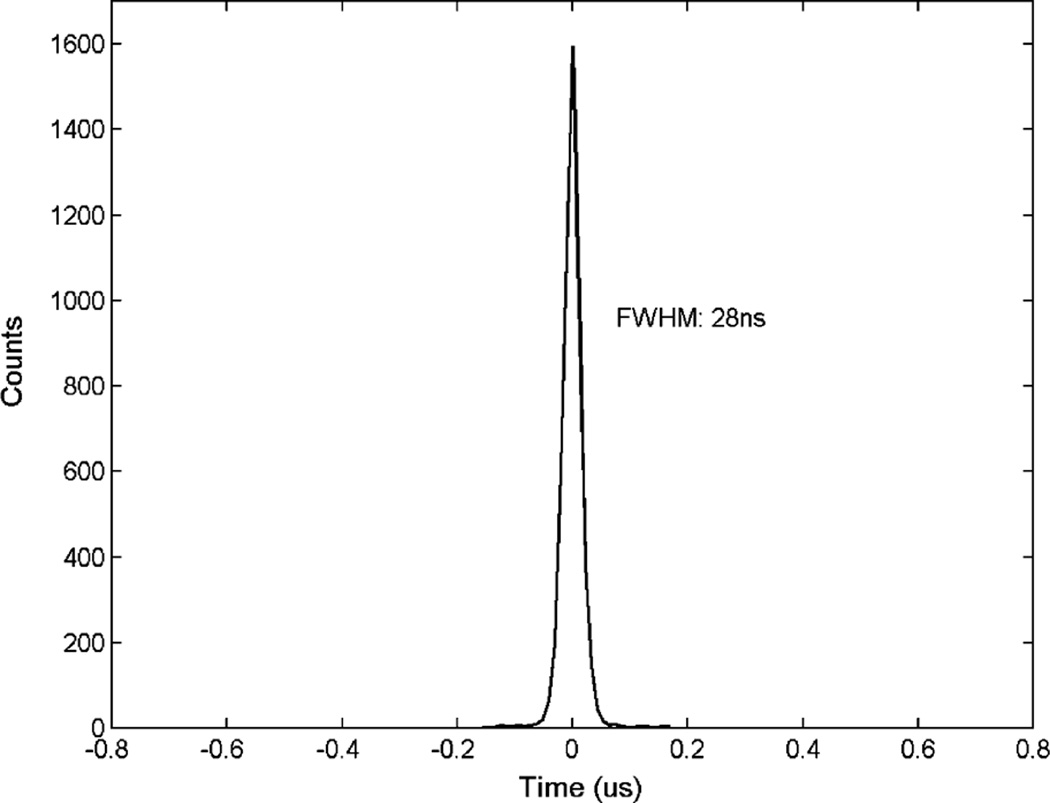
We can correct for this effect using methods very similar to that used in Section 3.1. We derived the mean bias for events corresponding to a small range of CAR and then subtracted this bias from all corresponding data points. This gave an overall time spread that depends much less on the depths of interactions. The distribution of estimated interaction times after this correction is shown in Fig. 14. The effect of this correction on the final timing spectra is shown in Figs. 15 and 16. The FWHM timing resolution was improved from 39 ns to 28 ns.
Fig. 14.
Distribution of estimated interaction time after correcting for depth dependence.
Fig. 15.
Timing spectrum measured with 600 ns falling edge, double exponential mode and full energy events. No correction for depth dependence was applied.
Fig. 16.
Timing spectrum measured with 600 ns falling edge, double exponential mode and full energy events and depth correction.
3.4. Measured timing resolution with finer sampling
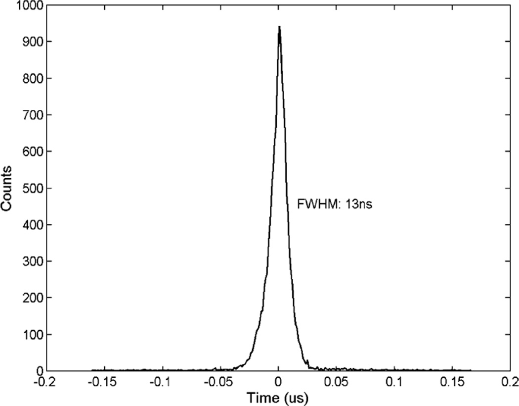
To further improve the timing estimation, we acquired 1 million events using the digital oscilloscope with its maximum sampling rate. Each recorded waveform has 8000 sample points at 1 ns sampling intervals. We first used all full energy events and repeated the procedures in previous sections to find out the optimum configuration for timing estimation. In this comparison, the double exponential model with 600 ns fall edge produced the best accuracy, as shown in Fig. 17. After depth correction, we obtained a timing resolution of 13 ns FWHM (Fig. 18). Note that by increasing the sampling rate from 200 MHz to 1 GHz, we see an improvement in timing accuracy by a factor of 2. We expect that this accuracy can be further improved if hardware with a higher sampling rate is available, until a stage in which the benefit of a higher sampling rate is offset by the non-linearity of the sampling. Finally, we repeated these procedures with all events that have energy depositions greater than 250 keV in the detector. This gave a measured timing resolution of 15 ns FWHM. In Table 3, we summarized measured timing resolutions with different experimental configurations.
Fig. 17.
Comparing waveform models and effective lengths fall edge for timing estimation.
Fig. 18.
Measured timing spectrum using double exponential model, 600 ns falling edge, and depth correction. A 13 ns FWHM timing resolution is achieved.
Table 3.
Measured timing resolutions using difference configurations
| Configuration | All events | 511 keV events with no correction |
511 keV events with correction |
>250 kV events with correction |
|---|---|---|---|---|
| Linear model, 500 ns fall edge 5 ns/sample | 60 ns | 54 ns | 38 ns | — |
| Double experimental/model, 600 ns fall edge 5 ns/sample |
— | 39 ns | 28 ns | — |
| Double experimental model, 600 ns fall edge 1 ns/sample |
— | 21 ns | 13 ns | 15 ns |
| Digital shaping & triggering 5 ns/sample | — | — | 74 ns | — |
4. Conclusions and discussions
In this work, the possibility of using pulse waveforms for interaction timing estimation was explored. A statistical description of the pulse waveform model is provided. We experimentally compared different configurations for extracting timing information. Some results are summarized as the following:
The digital shaping and triggering scheme did not provide sufficiently accurate interaction timing information. This is due to (a) the low charge carriers mobility in HgI2 and (b) fluctuations on the charge drifting/collection time.
A double exponential model, based on Hecht’s relation, provided the best timing accuracy.
A 13 ns FWHM timing resolution was achieved with 511 keV gamma rays and 1GHz sampling rate. Further improvement is expected with improved sampling rate and precision.
Mismatching between the simple models used and the actual waveforms produced systematic error in the timing estimation. This effect was compensated to a certain extent as shown in our results. A better approach may be building those factors, causing the mismatching, into waveform models, so that their effects can be minimized. This, however, requires not only a better understanding of the detector responses but also more complicated waveform models. Further study along this line may be required.
In our current approach, the timing information was derived using iterative WLS fitting. This limits the data rate that can be handled with current computing hardware. The computation time can be greatly reduced if one uses pre-defined models that take into account the experimentally derived waveform characteristics along with non-iterative estimation methods. One can experimentally obtain a “detector timing response function” that contains the expected waveforms for every given interaction depth and energy deposition. Once this information is available, we can use a much simpler and faster timing estimation scheme to find the interaction time. Deriving such a response function would require a thorough and time consuming experimental mapping of the detector response.
APPENDIX I. Covariance of cathode waveform
We start from considering only carriers of a single polarity. Assuming the carriers were generated at time 0, the covariance between the induced charge Q(t) and Q(t + u) at time t and t + u, due to charge carrier generation and drifting process, is defined as
| (1) |
In order to evaluate the covariance, one may start from the conditional covariance given N0 carriers were initially generated and N(t) survived after a drifting period of length t,
| (2) |
where A(u) is the mean weighting potential change induced by a single charge carrier within a period u,
| (3) |
After a few simple steps of derivation, we get
| (4) |
Note that the integral in the last step is the conditional variance of the induced charge at time t. Substituting (1) into (3), and further averaging over N(t), we get
| (5) |
At this point, we take into account both electron and hole contributions. Given N0, the drifting of electrons and holes are completely independent. Therefore, the overall contribution of electrons and holes to the covariance of the waveform, conditional on N0, is
| (6) |
From this, one can get the covariance of the waveform by integrating over N0,
| (7) |
where F is the Fano factor and τ is the mean free time for the charge carriers. Ae(u) and Ah(u) are the mean weighting potential changes by a single moving electron or hole within a given drifting time u, as defined in (3).
References
- 1.Sharma SL, Acharya HN. Bull. Mater. Sci. 2002;25(2):85. [Google Scholar]
- 2.Alexiev D, Dytlewski N, et al. Nucl. Instr. and Meth. A. 2004;517(1–3):226. [Google Scholar]
- 3.Baciak JE, He Z. IEEE Trans. Nucl. Sci. 2003;NS-50(4):1220. [Google Scholar]
- 4.Baciak JE, He Z. Nucl. Instr. and Meth. A. 2003;505(1–2):191. [Google Scholar]
- 5. http://www.amptek.com/a250.html. [Google Scholar]
- 6.Barrett HH, Eskin JD, et al. Phys. Rev. Lett. 1995;75(1):156. doi: 10.1103/PhysRevLett.75.156. [DOI] [PubMed] [Google Scholar]
- 7.Knoll GF. Radiation Detection and Measurement. third. New York: Wiley & Sons; 1999. p. 480. ISBN 0-470-07338-5. [Google Scholar]
- 8.Eskin JD, Barrett HH, et al. J. Appl. Phys. 1999;85(2):647. [Google Scholar]
- 9.Owens A, Bavdaz M, et al. Nucl. Instr. and Meth. A. 2002;479(2–3):535. [Google Scholar]


