Abstract
Two-dimensional molybdenum disulfide (MoS2) is a promising material for ultrasensitive photodetector owing to its favourable band gap and high absorption coefficient. However, their commercial applications are limited by the lack of high quality p-n junction and large wafer scale fabrication process. A high speed Si/MoS2 p-n heterojunction photodetector with simple and CMOS compatible approach has been reported here. The large area MoS2 thin film on silicon platform has been synthesized by sulfurization of RF-sputtered MoO3 films. The fabricated molecular layers of MoS2 on silicon offers high responsivity up to 8.75 A/W (at 580 nm and 3 V bias) with ultra-fast response of 10 μsec (rise time). Transient measurements of Si/MoS2 heterojunction under the modulated light reveal that the devices can function up to 50 kHz. The Si/MoS2 heterojunction is found to be sensitive to broadband wavelengths ranging from visible to near-infrared light with maximum detectivity up to ≈1.4 × 10¹² Jones (2 V bias). Reproducible low dark current and high responsivity from over 20 devices in the same wafer has been measured. Additionally, the MoS2/Si photodetectors exhibit excellent stability in ambient atmosphere.
Transition metal dichalcogenides (TMDs) are predicted to be promising candidate for next generation electronics1,2,3, optoelectronics4,5, and sensor6 devices. The intrinsic nature of carriers in two dimensional semiconductors offers numerous advantages such as high mobility, high sensitivity, fast response and chemical stability7,8,9,10. Among several of the layered TMDs, MoS2 has attracted great interest because of its distinctive electronic, optical, and catalytic properties4,5,6,9,10,11,12. In the recent time a lot of efforts have been devoted to demonstrate the potential of MoS2 for a variety of applications13,14,15. MoS2 has been used as an active layer in high mobility transistors (70–100 cm2/V-s) with very high on/off ratio of 108 16,17. More importantly, the broad spectrum from which MoS2 can absorb light i. e. visible to near-infrared spectral region (350–950 nm) is higher than GaAs and Si (one order of magnitude in a thickness of less than 1 nm) which makes it an ideal material for photonic devices18,19. However, the use of MoS2 for practical applications is still limited due to the lack of scalability in its fabrication process. Several methods such as mechanical/chemical exfoliation, chemical vapour deposition etc20,21,22,23. that have been reported are mired with drawbacks. In the exfoliation method, poor control over thickness and limited size of MoS2 films are the main deterrents. On the other hand there are reports available, where large-area MoS2 layers has been directly obtained using chemical vapour deposition and solution processed methods4,24,25. The absence of high quality p–n junctions also limits the performance of the MoS2 based devices. Although photodetectors based on mono/multilayer MoS2 heterostructure have shown excellent device characteristics in terms of high sensitivity (up to 7 A/W) and wide band response26,27,28,29 their applicability still suffers due to complex fabrication process.
In this work, we report Si/MoS2 (p-n) heterojunction based photodetector contrived from a very simple, reproducible and scalable fabrication process. To fabricate the heterojunction, we have adopted CVD process for the growth of MoS2 thin film as mentioned in previously published reports24,26. The durability and scalability of the devices examined after two months are found to remains intact. The fabricated heterojunction exhibited excellent photoresponse properties in the visible to near-infrared wavelengths with a maximum responsivity of 8.75A W−1 and fast rise time of 10 μs. The excellent performance of multilayered MoS2 heterostructure may lead the way for the fabrication of high speed photodetectors.
Experimental details
Synthesis of large area MoS2 thin film
In the present study, MoS2 thin films were fabricated by the sulphurization of molybdenum trioxide (MoO3) in N2 ambient at low temperature. In a typical process, a 10 nm thick film of MoO3 was first deposited on the SiO2/Si substrates by reactive sputtering (in presence of Ar and O2 with 1:1 ratio). The MoO3/SiO2/Si samples were then placed at the centre of a tube furnace preheated to 500 °C and maintained for 20 min. Sulphur powder was introduced in the upstream zone of the furnace, where temperature is around 200 °C. As a result of the sulphurization process, thin films of MoS2 with large area coverage were grown. The structural and morphological properties of deposited samples were characterized by Scanning electron microscopy (SEM- Ziess evo 18), and atomic force microscopy (AFM- Bruker dimension). In order to confirm the formation of MoS2 Raman spectroscopy (Horiba Raman Lab RAM HR 800 Evolution) has been employed.
Device fabrication and measurements
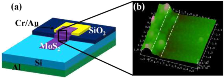
Si/MoS2 heterojunction photodetectors were fabricated using C-MOS compatible technology. P-type silicon (100) with a thermally grown silicon oxide (SiO2) of 100 nm was used as the starting wafer for the fabrication of Si/MoS2 heterojunction. To expose the silicon, SiO2 was selectively etched after the first UV-lithography step. A two step photo-lithography process has been used to make the heterojunction. In the first step, squares of dimension 100 μm2 were opened in SiO2, which define the Si/MoS2 junction area. The metal contact (Cr/Au) has been patterned in the second lithography process. The detailed fabrication process is given in the supplementary information (Fig. S1). On the top of this structure, thin layer of MoO3 (10 nm) was deposited by reactive sputtering. Samples were cleaned in the oxygen plasma for 30 sec before the deposition of MoO3. After the deposition of MoO3, MoS2 was grown via sulphurization process discussed earlier. Cr/Au layers on the top serve as the one electrode for the electrical measurements, while a 100 nm thick layer of Al has been deposited on the back side of the silicon for second electrode. Figure 1(a) shows a typical schematic representation of the device structure. MoS2 thin film on Si and metal contact can be seen in the AFM image Fig. 1(b). In order to measure the photoresponse of Au-MoS2-Au metal-semiconductor-metal (MSM) photodetector was fabricated. The fabrication process was the same as Si/MoS2 heterojunction, except that the bottom oxide was not etched. Electrical measurements of the device were performed using Keithley semiconductor analyzer (SCS4200) under ambient conditions. The spectral response of the photodetector has been measured in the wavelength range 300 nm to 1100 nm.
Figure 1.
Schematic representations of the Si/MoS2 p-n heterojunction photodetector, (b) AFM image of MoS2 layer at metal contact and heterojunction interface.
Results and Discussion
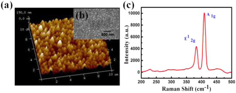
The morphology of the as deposited MoS2 film surface observed under an atomic force microscopy (AFM) is shown in Fig. 2(a). The surface of the film seems to be composed of vertically aligned nanoflakes with average width between 20–40 nm. It is likely that these stratified features in the MoS2 thin film formed as a result of the difference in the thermal expansion coefficient of substrate and the MoS2 film during sulfurization. The growth of MoS2 film was homogenous and it covered the entire substrate surface (~2inch) uniformly. Similar growth has been observed by Ellmer et al.30 and S. B, Sadale et al.31 in case of WS2. A Scanning electron microscope (SEM) image of the as synthesized MoS2 is shown in the inset of Fig. 2(a). The above SEM image confirms clearly the formation of nanoflakes of MoS2. Similar morphology of MoS2 surfaces has also been observed on SiO2 substrate (Fig. S2(b) supplementary information). It is believed that this morphology originates from the hexagonal basal plane symmetry of the MoS2 crystal itself, suggesting that the layers grown are oriented along c-axis of the MoS2 unit cell24,32. A crystallinity of the MoS2 thin film samples were examined using Raman spectroscopy (514 nm laser and 10 mW power). The characteristic Raman peaks for the E12g and A1g vibration modes appeared at 384 cm−1 and 408 cm−1 corresponding to MoS2 hexagonal phase, as shown in Fig. 2(c)24,32. The overall intensity of the peaks and the relative ratio, of the E1 2 g, the A1g peaks were similar to that from high quality exfoliated MoS2. The crystallinity of the MoS2 thin film was further investigated by XRD spectra (shown in Fig. S2(c) supplementary information). The preferred direction of growth was found to be along the c-axis (0001) of hexagonal phase24,32,33. This suggests that these films were of good structural quality.
Figure 2.
(a) AFM image and (b) Raman spectra of as synthesized MoS2.
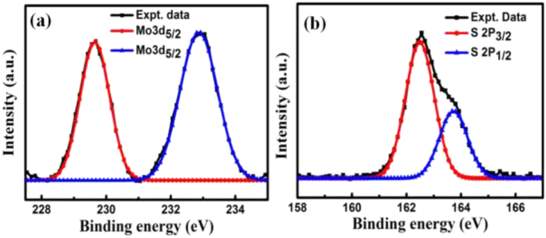
The chemical bonding and electronic properties of the MoS2 films were investigated by X-ray photoelectron spectroscopy (XPS) using Al–Kα radiation of energy 1486.6 eV. Binding energies of Mo 3d and S 2p electrons are shown in Fig. 3(a,b). Two distinct peaks for Mo 3d electrons observed at 229.4 and 232.6 eV were attributed to 3d5/2 and 3d3/2 chemical states, respectively34,35,36,37,38. The possibility of Mo-silicide or migration of Mo in Si was investigated by comparing the XPS peaks of Mo and Si with that reported in literature. The silicide related peaks of Mo are reported at lower binding energies for 3d5/2 and 3d3/235,36. Similarly the XPS peak of Si 2P3/2 was observed at 99.4 eV, which gets shifted towards lower binding energy for the Mo-silicide formation. In our samples the peak position of Si 2P3/2 has been observed at 102.3 eV35,36 (Fig. S2(a) in supplementary information). XPS analysis for both of the Mo and Si clearly confirmed that formation of silicide or migration of Mo in Si has not occurred in our samples. The spectrum for S 2p electrons is resolved into Gaussian peaks located at 162.5 eV and 163.8 eV, owing to S 2p3/2 and S 2p1/2 states, respectively. The observed peak positions of spin-orbit coupled Mo 3d and S 2p electrons are in excellent agreement with those reported in literature33, confirming the synthesis of pure hexagonal 2-H phase MoS2.
Figure 3.
(a) and XPS spectra showing the binding energy of (a) Mo 3d and (b) S 2p electron.
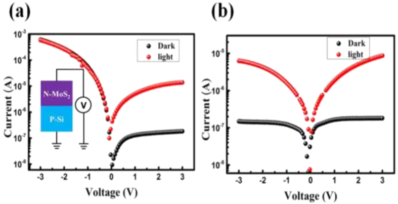
In general bulk MoS2 exhibit n-type conductivity and makes a type –II p-n junction with the p-Si. Since the Raman spectra from the as-synthesized MoS2 sample shows a splitting of more than 25 cm−1 between E12g (384 cm−1) and A1g (408 cm−1) modes, which is similar to bulk (multilayered) structure34,36,37,38,39. A typical current-voltage (I–V) characteristic of the Si/MoS2 heterojunction under the light and dark condition is depicted in Fig. 4(a). During the measurement, the p-type substrate was kept at ground and the bias voltage was applied to the top MoS2 contact and therefore a negative voltage to the top contact would make the junction forward biased. The voltage biasing scheme is shown in the inset of Fig. 4(a). The high asymmetry observed in the I–V characteristics clearly indicates the formation of a very good p-n junction between the n-type MoS2 and p-type Si. A dark current of ~1.8 × 10⁻⁷was measured at reverse bias of 3 V, which enhances ~127 times upon illumination under 560 nm light of intensity 5 mW/cm2. In order to estimate the ideality factor η of the fabricated heterojunction, the semi-log J-V plot has been fitted according to the following equation18,34.
Figure 4.
I-V characteristics of (a) Si-MoS2 p-n heterojunction and (b) Au/MoS2/Au MSM photodetector.
 |
Here q is the unit charge, kB is the Boltzmann’s constant, and J is current density. Current density (J) versus voltage (V) plot of the n-MoS2 and p-Si heterojunction is given in the supplementary information (Fig. S3(a)). The diode ideality factor is found to be ~2.4. Since no passivation layer exists at the MoS2-Si interface, the relatively large ideality factor might have originated due to the existence of interface defects states34. Furthermore, the I-V curve of the heterojunction in the dark could be described by thermionic emission theory of charge carriers over a potential zero bias barrier Φb, from the Si to MoS2. Φb can be defined by the following equation18.
 |
Here A is the area (100 × 100 μm2) of the device, A* (32 A cm−2K−2 for p-Si) is the effective Richardson constant. Based on the above equations, Φb was estimated to be approx. 0.545 eV. The C–V measurement on this heterojunction has been carried out and has been added as Fig. S3(b) in supplementary information. The used p-silicon wafers were boron doped with ~1015 cm−3. From the C–V analysis the doping concentration for MoS2 of ~2 × 1016 cm−3 was extracted for C-V analysis. Photoresponse of MoS2 MSM photodetector was measured under the same illumination level to compare the performance with the MoS2-Si p-n junction. Figure 4(b) shows the IV characteristics of Au- MoS2-Au MSM photodetector. The measured dark current for MSM photodetector was found to be ~2.5 × 10⁻⁷ (at reverse bias of 3 V). Upon illumination (560 nm) a photo-to-dark current ratio of ~72 is achieved. For a better comparison MSM photodetector with one side Au and one side ohmic (low work function metal Ag) contact was made. I-V characteristic of Au-MoS2-Ag is shown in Fig. S4(a). Semi ohmic nature (low rectification ratio of ~4) indicates the low barrier height of Au-MoS2 contact39. Additionally the photocurrent the two MSM photodetectors are not much different from each other (Fig. (S4(b)). From these results it can be easily noted that the MoS2-Si heterojunction possess larger gain than the MoS2 MSM photodetector. The high rectification ratio, low turn-on voltage, and small ideality factor coupled with high photoresponse clearly demonstrate the high quality of the fabricated heterojunction photodetector.
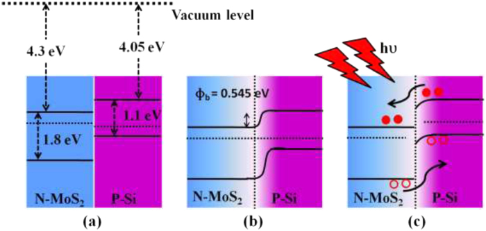
The conduction mechanisms behind the operation of Si/MoS2 heterojunction photodetectors can be explained using the help of energy band diagrams, as shown in Fig. 5. The alignment of the conduction and valence band edges of Si and MoS2 in proper energy scale, is shown in Fig. 5(a). Under an equilibrium condition (zero bias), the band diagram of the MoS2-Si heterojunction would be as shown in Fig. 5(b), where an electron affinity of 4.3 and a band gap of 1.8 for MoS2 was assumed34,40. Since the thickness of MoS2 layer is around 4–6 nmit would be fully depleted. As a result no bend bending in the energy band diagram in MoS2 is expected as shown in Fig. 5(b). When the junction is formed between p-type Si with a work function (Φ Si) of 4.9 eV and n-type MoS2 (Φ MoS2 ~ 4.7 eV)34, a large barrier potential would be created at the MoS2/Si interface. On applying a reverse bias, the Ef (p-Si) is lifted to higher values, as shown in Fig. 5(c). That in turn enhances the electric field across the depletion region gradually and results in the expansion of barrier potential as well. This will open up a large number of accessible states for the holes to be injected into Si region. Here the higher carrier mobility of MoS2 also helped to enhance the photoresponse of the photodetector. Under light illumination, electron–hole pairs are generated, which are then separated by this large barrier potential and collected by the electrodes. As a result of that photocurrent, which was totally suppressed near V ≈ 0, significantly improves under small reverse bias.
Figure 5.
(a) Band edge alignment of Si/MoS2 heterostructure and band diagram of MoS2-Si heterojunction (b) at 0 V bias (c) at reverse bias.
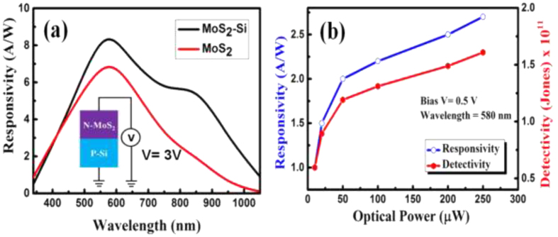
Next, the photoresponse from Si/MoS2 heterojunction and MoS2 MSM devices were measured within the wavelength range 350 nm to 1050 nm. Spectral responsivity of a photodetector is directly proportional to the internal gain and it represents the efficiency of a detector for the specific optical signals. Responsivity of a photodetector can be defined as follows40,41,42,43.
 |
Here IL and Id are the current under light and dark condition, while Pin is the incident optical power density. Figure 6(a) shows the spectral response from the MoS2/Si heterojunction and MoS2 MSM device at a bias of 3 V. Boththe devices register a wide spectral response, for wavelength ranging from 450 nm–1000 nm. Two prominent peaks centered around 580 nm and 860 nm were observed for Si/MoS2 heterojunction. On the other hand, for MoS2 MSM photodetector, a single the peak was observed at 580 nm. It can therefore be concluded that the high responsivity at 580 nm is due to the absorption of MoS2 film in the visible region34. The other peak at a wavelength of 860 nm corresponds to conventional Si based photodiode, which was observed from the absorption of the Si substrate42. As can be seen from Fig. 6(a), the responsivity for the MoS2 MSM photodetector in the longer wavelength range (greater than 600 nm) is relatively lower than Si/MoS2 heterojunction, due to the absence of Si junction. The improved photoresponse from MoS2-Si device can be explained as follows. The introduction of the p-n heterojunction in the MoS2/Si photodetector leads to the formation of an inherent large barrier height (depletion region) which gets further enhanced under a reverse bias. Under light illumination, electron–hole pairs are generated, which then gets separated by the large electric field and are collected at electrodes. The performance MoS2/Si heterojunction photodetector also has contribution from the surface morphologies of deposited MoS2 film. The photo-carrier generation and collection efficiency might have been enhanced due light trapping phenomena and high photosensitivity from the textured feature (nanostructures) at the surface. The high mobility of carrier in MoS2-Si p-n junction due to high electric field might be another of the contributing factor. The value of responsivity for MoS2-Si and MoS2 MSM photodetector as shown in Fig. 6(a) measured at 580 nm are 8.50 A/W and 6.8 A/W respectively. It is known that high reflection losses reduces the responsivity at smaller wavelengths, while for the longer wavelengths, reduction in responsivity is caused by band gap limit. Apart from responsivity (R), the performance of any photodetector can be expressed by detectivity (D*). These two characteristics properties are related to each other according to following equation4,18,34.
Figure 6.
(a) responsivity of Si/MoS2 heterojunction and MoS2 MSM photodetector (inste shows the biasing condition for Si/MoS2 heterojunction) and (b) optical power density dependent responsivity and detectivity of Si/MoS2 heterojunction photodetector.
 |
Detectivity represents the ability of a detector to detect weak optical signals, which has been calculated from the above equation. It is assumed that the dark current is dominated by the shot noise for estimating detectivity. The other sources of noise (Johnson and flicker noise) are mainly thermal fluctuations, which can be neglected. Equation (4) suggests that a low dark current and a high responsivity are desired for the photodetector to exhibit high detectivity. The peak detectivity of the fabricated p-n heterojunction diode is estimated to be ~2 × 1011 cm-Hz1/2. W−1 (or Jones) at 0.5 V bias, which get enhanced up to ~1.4 × 10¹² Jones for 2 V bias. High detectivity indicates that the MoS2-Si heterojunction is extremely sensitive to small optical input signals. The order of detectivity found in this work is high compare to other reported MoS2-based photodetectors4,7,18,34. Most importantly, the high D* is acquired at small external bias voltage (0.5 V), in contrast to the relatively high bias voltage needed in previous works4,18,34. Figure 6(b) shows the linear increase of both responsivity and detectivity for low power illumination, and a a sub-linear dependence at higher power levels. The increase of illumination intensity leads to the enhanced electron–hole pair generation rate, resulting in a higher photocurrent. Under weak light intensity, the photogenerated electrons in MoS2 will be captured by the trap states. As a result of reduced recombination, the lifetime for the photogenerated holes can be greatly prolonged, leading to higher R and D*. However, the available states will be remarkably reduced with increasing light intensity, eventually causing the saturation of photoresponse34. The sub-linear behaviour of the responsivity and detectivity (Fig. 6(b)) indicates that trap states in the MoS2 layer or at the junction interface is responsible for this phenomenon.
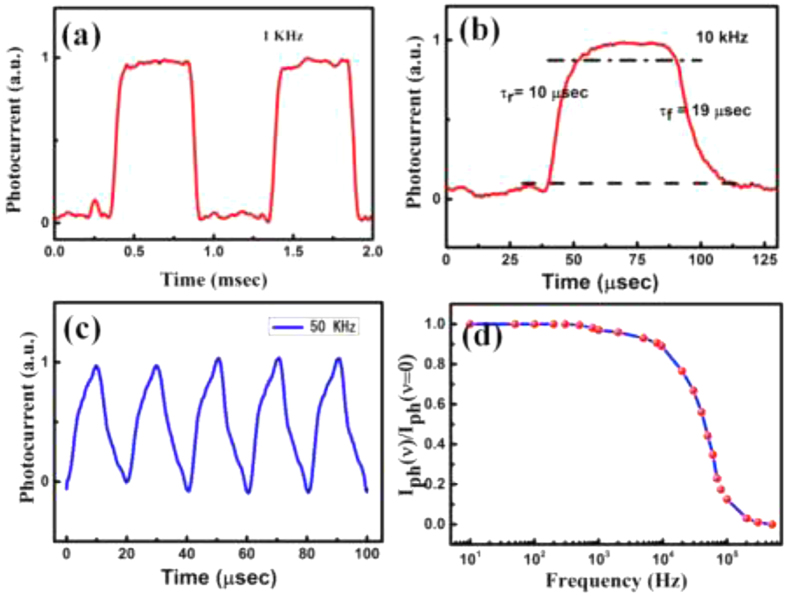
Transient measurements of Si/MoS2 junction under different illumination level are shown in Fig. S4 (supplementary information). The steep rise and fall edges suggest a fast response speed, indicating that electron–hole pairs could be effectively generated and separated in the Si/MoS2 heterojunction. To further investigate the response time of MoS2-Si heterojunction, transient measurements were performed under the illumination of modulating light source. A modulated laser source of wavelength 660 nm was used for these experiments. Response of the fabricated devices has been extracted in terms of the voltage across a resistance of 100 KΩ connected to the device (in series). The schematic representations of measurement setup and time response characteristics (for 10 kHz modulation) are given in the supplementary information (Fig. S4). The measurements have been carried out with a modulation up to 50 kHz of laser source. Figure 7(a) shows the time response of Si/MoS2 photodetector under the 1 kHz modulated light. In the time domain, the speed of a PD is often characterized by the rise time (τr, the time interval from10% to 90% of the maximum photocurrent) and the fall time (τf, the time interval from 90% to 10% of the maximum photocurrent) of its response to an impulse signal. The magnified plot of time response for one cycle is shown in Fig. 7(b). Further analysis reveals a small τr of 10 μs, as well as a small τf of 19 μs. The values obtained here are remarkably high and much faster than any other reported MoS2-based PDs Time response of the Si/MoS2 heterojunction for 50 kHz laser modulation is also shown inset of Fig. 7(c). The high performance of the photodetector could be ascribed to the following aspects. First, the existence of a strong build-in electric field at the MoS2 and Si interface can greatly facilitate the separation and transport of photo-generated carriers. This leads to the large response and relatively high speed of the heterojunction. Second aspects is the high in-plane mobility of carriers in the MoS2 layer, which offers high speed paths for the transport of photogenerated carriers in this vertically standing layered structure. For 100 K ohm load resistance the cut off frequency obtained from the following eq. (5) should be 33.3 kHz.
Figure 7.
Time response characteristics under modulated light (a) 1 kHz, (b) 10 kHz (magnified), (c) 50 kHz and (d) Frequency dependence of normalized relative change in photocurrent (Iph(υ)/Iph(0)).
 |
This high cut off frequency reflects in the high speed operation of the present device. The relative change in the current (Iph(υ)) of the photocurrent as a function of frequency in the range from 10 to 500 kHz is shown in Fig. 7(d). The relative change (defined as Iph(υ) = IL − Id)of the photocurrent only decreases by 50% at a high frequency of ≈40 kHz, implying that the Si/MoS2 based PDs can operate at much higher frequencies. A comparison of improved performances of our Si/MoS2 heterostructure has been given in Table 1 with other MoS2 based photodetectors.
Table 1. A Comparison of the performance of MoS2 and heterojunction based photodetector.
| PDs structure (Device area) | Responsivity (A/W) | Response time(τr/τf) | Detectivity (Jones) | Ref. |
|---|---|---|---|---|
| MoS2 Schottky MSM PDs | 1.04 A W−1 | 40/50 μs | 22 | |
| Si/MoS2 heterojunction | 7 | 50/50 ms | 1010 | 29 |
| MoS2-QD/Si heterostructure | 2.8 | - | 0.8 × 10¹² | 34 |
| Si/MoS2 heterojunction (5 × 5 μm2) | 11.9 | 30.5/71.6 μs | — | 4 |
| MoS2 Schottky MSM PDs | 0.55- 1 | 0.2/1.7 ms | — | 13 |
| Si/MoS2 heterojunction (10 × 10 μm2) | 0.210 | 0.3/0.3 ms | — | 40 |
| Si/MoS2 heterojunction | 8.75 A/W | 10/19 μs | 1.4 × 10¹² | This Work |
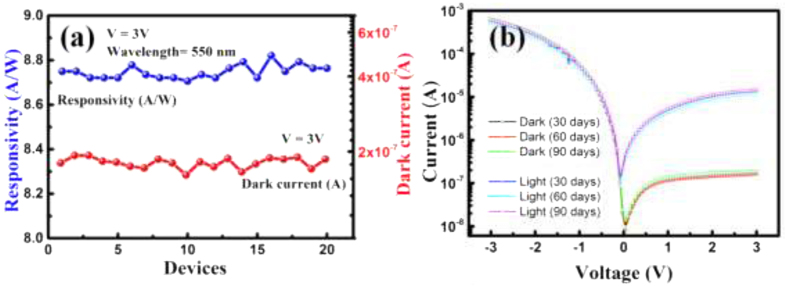
The scalability of the process has also been investigated. Twenty devices has been fabricated and tested on the same substrate. The responsivity and dark current variation of these devices are shown in Fig. 8(a). A negligible differences in the responsivity and dark current shows the reproducibility of the measurements, which reflects in the high scalability of the fabrication process. Similarly the scalability of Au-MoS2-Au MSM photodetector was also investigated. The responsivity and dark current measurements for the 20 devices fabricated on the same substrate are presented in supplementary information. Furthermore, we investigated the air stability of the Si/MoS2 photodetector by exposing it directly in air for more than three months without any encapsulation and found the similar results. Figure 8(b) shows I-V characteristics of Si/MoS2 under normal ambient conditions. The device has been tested for consecutive three months and shows good atmospheric stability.
Figure 8. Scalability and stability test.
(a) responsivity and dark current of 20 devices fabricated in simultaneously on single substrate, (b) I-V characteristics of Si/MoS2 photodetector for different time period.
Conclusion
Si/MoS2 heterojunction was fabricated by depositing MoS2 films with a vertically standing layered structure on p-type silicon. MoS2 layer was grown on wafer scale using the sulphurization MoO3 thin films. The devices exhibit excellent photosensitive characteristics such as large responsivity (~8.75 A/W for 580 nm at 3 V bias), high detectivity (~1.4 × 10¹² Jones for 2 V bias) and very fast time response of 10 μsec. Transient measurements reveal that our photodetector exhibits excellent stable and reproducible dynamic response upon high frequency pulsed light, enabling it suitable for high-frequency or high-speed optical- switch applications. Moreover, the combination of reproducible and scalable fabrication process used in this work should be suitable for multiplexed photodetector arrays.
Additional Information
How to cite this article: Dhyani, V. and Das, S. High-Speed Scalable Silicon-MoS2 P-N Heterojunction Photodetectors. Sci. Rep. 7, 44243; doi: 10.1038/srep44243 (2017).
Publisher's note: Springer Nature remains neutral with regard to jurisdictional claims in published maps and institutional affiliations.
Supplementary Material
Acknowledgments
The authors would like to thank Department of Electronics and Information Technology (DEITY) and Department of Science and Technology (DST) for their financial support. We are very grateful to the Nanoscale Research Facility (NRF), IIT Delhi for providing assistance in the fabrication and characterization facilities.
Footnotes
The authors declare no competing financial interests.
Author Contributions V.D. conducted all the experimental works. V.D. and S.D. wrote the manuscript and assisted the interpretation of measurement data. All authors reviewed themanuscript.
References
- Ganatra R. & Zhang Q. Few-Layer MoS2: A Promising Layered Semiconductor. Acs Nano 8, 4074–4099 (2014). [DOI] [PubMed] [Google Scholar]
- Mak K. F., Lee C., Hone J., Shan J. & Heinz T. F. Atomically Thin MoS2: A New Direct-Gap Semiconductor. Phys. Rev. Lett. 105, 136805 (2010). [DOI] [PubMed] [Google Scholar]
- Gupta A., Sakthivel T. & Seal S. Recent development in 2D materials beyond graphene. Prog. Mater. Sci. 73, 44–126 (2015). [Google Scholar]
- Zhang Y. et al. In Situ Fabrication of Vertical Multilayered MoS2/Si Homotype Heterojunction for High-Speed Visible-Near-Infrared Photodetectors. Small Weinh. Bergstr. Ger. 12, 1062–1071 (2016). [DOI] [PubMed] [Google Scholar]
- Mak K. F. & Shan J. Photonics and optoelectronics of 2D semiconductor transition metal dichalcogenides. Nat. Photonics 10, 216–226 (2016). [Google Scholar]
- Cho B. et al. Charge-transfer-based Gas Sensing Using Atomic-layer MoS2. Sci. Reports 5, 8052 (2015). [DOI] [PMC free article] [PubMed] [Google Scholar]
- Li X. et al. High Detectivity Graphene-Silicon Heterojunction Photodetector. Small 12, 595–601 (2016). [DOI] [PubMed] [Google Scholar]
- Bhimanapati G. R. et al. Recent Advances in Two-Dimensional Materials beyond Graphene. Acs Nano 9, 11509–11539 (2015). [DOI] [PubMed] [Google Scholar]
- Riazimehr S. et al. Spectral Sensitivity of Graphene/Silicon Heterojunction Photodetectors. Solid-State Electron. 115, 207–212 (2016). [Google Scholar]
- Butler S. Z. et al. Progress, Challenges, and Opportunities in Two-Dimensional Materials Beyond Graphene. Acs Nano 7, 2898–2926 (2013). [DOI] [PubMed] [Google Scholar]
- Dolui K., Rungger I. & Sanvito S. Origin of the n-type and p-type conductivity of MoS2 monolayers on a SiO2 substrate. Phys. Rev. B 87, 165402 (2013). [Google Scholar]
- Li H. et al. Optical Identification of Single- and Few-Layer MoS2 Sheets. Small 8, 682–686 (2012). [DOI] [PubMed] [Google Scholar]
- Lu J. et al. Improved Photoelectrical Properties of MoS2 Films after Laser Micromachining. Acs Nano 8, 6334–6343 (2014). [DOI] [PubMed] [Google Scholar]
- Zu S. et al. Active Control of Plasmon–Exciton Coupling in MoS2–Ag Hybrid Nanostructures. Adv. Opt. Mater. doi: 10.1002/adom.201600188 (2016). [DOI] [Google Scholar]
- Lopez-Sanchez O., Lembke D., Kayci M., Radenovic A. & Kis A. Ultrasensitive photodetectors based on monolayer MoS2. Nat. Nanotechnol. 8, 497–501 (2013). [DOI] [PubMed] [Google Scholar]
- Wang H. et al. Integrated Circuits Based on Bilayer MoS2 Transistors. Nano Lett. 12, 4674–4680 (2012). [DOI] [PubMed] [Google Scholar]
- Nourbakhsh A., Zubair A., Dresselhaus M. S. & Palacios T. Transport Properties of a MoS2/WSe2 Heterojunction Transistor and Its Potential for Application. Nano Lett. 16, 1359–1366 (2016). [DOI] [PubMed] [Google Scholar]
- Wang L. et al. MoS2/Si Heterojunction with Vertically Standing Layered Structure for Ultrafast, High-Detectivity, Self-Driven Visible–Near Infrared Photodetectors. Adv. Funct. Mater. 25, 2910–2919 (2015). [Google Scholar]
- Bernardi M., Palummo M. & Grossman J. C. Extraordinary sunlight absorption and one nanometer thick photovoltaics using two-dimensional monolayer materials. Nano Lett. 13, 3664–3670 (2013). [DOI] [PubMed] [Google Scholar]
- Li H., Wu J., Yin Z. & Zhang H. Preparation and Applications of Mechanically Exfoliated Single-Layer and Multilayer MoS2 and WSe2 Nanosheets. Accounts Chem. Res. 47, 1067–1075 (2014). [DOI] [PubMed] [Google Scholar]
- Lembke D., Bertolazzi S. & Kis A. Single-Layer MoS2 Electronics. Accounts Chem. Res. 48, 100–110 (2015). [DOI] [PubMed] [Google Scholar]
- Tsai D. S. et al. Trilayered MoS Metal SemiconductorMetal Photodetectors: Photogain and Radiation Resistance. IEEE J. Sel. Top. Quantum Electron. 20, 30–35 (2014). [Google Scholar]
- Tsai M.-L. et al. Monolayer MoS2 Heterojunction Solar Cells. Acs Nano 8, 8317–8322 (2014). [DOI] [PubMed] [Google Scholar]
- Laskar M. R. et al. Large area single crystal (0001) oriented MoS2. Appl. Phys. Lett. 102, 252108 (2013). [Google Scholar]
- Alkis S. et al. Thin film MoS2 nanocrystal based ultraviolet photodetector. Opt. Express 20, 21815 (2012). [DOI] [PubMed] [Google Scholar]
- Lee Y.-H. et al. Synthesis of Large-Area MoS2 Atomic Layers with Chemical Vapor Deposition. Adv. Mater. 24, 2320–2325 (2012). [DOI] [PubMed] [Google Scholar]
- Kwak J. Y., Hwang J., Calderon B., Alsalman H. & Spencer M. G. Long wavelength optical response of graphene-MoS2 heterojunction. Appl. Phys. Lett. 108, 091108 (2016). [Google Scholar]
- Xue F. et al. p-Type MoS2 and n-Type ZnO Diode and Its Performance Enhancement by the Piezophototronic Effect. Adv. Mater. 28, 3391–3398 (2016). [DOI] [PubMed] [Google Scholar]
- Li Y., Xu C.-Y., Wang J.-Y. & Zhen L. Photodiode-Like Behavior and Excellent Photoresponse of Vertical Si/Monolayer MoS2 Heterostructures. Sci. Reports 4, 7186 (2014). [DOI] [PMC free article] [PubMed] [Google Scholar]
- Weiß V., Seeger S., Ellmer K. & Mientus R. Reactive magnetron sputtering of tungsten disulfide (WS2−x) films: Influence of deposition parameters on texture, microstructure, and stoichiometry. J. Appl. Phys. 101, 103502 (2007). [Google Scholar]
- Sadale S. B. & Patil P. S. Synthesis of type-I textured tungsten disulfide thin films on quartz substrate. J. Cryst. Growth 286, 481–486 (2006). [Google Scholar]
- Kumar P., Singh M., Sharma R. K. & Reddy G. B. An experimental study: Role of different ambient on sulfurization of MoO3 into MoS2. J. Alloys Compd. 671, 440–445 (2016). [Google Scholar]
- Lee E. W. et al. Growth and electrical characterization of two-dimensional layered MoS2/SiC heterojunctions. Appl. Phys. Lett. 105, 203504 (2014) [Google Scholar]
- Mukherjee S., Maiti R., Katiyar A. K., Das S. & Ray S. K. Novel Colloidal MoS2 Quantum Dot Heterojunctions on Silicon Platforms for Multifunctional Optoelectronic Devices. Sci. Reports 6, 29016 (2016). [DOI] [PMC free article] [PubMed] [Google Scholar]
- Shaw L. & Abbaschian R. Chemical states of the molybdenum disilicide (MoSi2) surface. J. Mater. Sci. 30, 5272–5280 (1995). [Google Scholar]
- Meng Q., Zhang J., Li Z., Li G. & Chen R. Synthesis of molybdenum silicide by both ion implantation and ion beam assisted deposition. Appl. Surf. Sci. 254, 2678–2684 (2008). [Google Scholar]
- Kibsgaard J., Chen Z., Reinecke B. N. & Jaramillo T. F. Engineering the surface structure of MoS2 to preferentially expose active edge sites for electrocatalysis. Nat. Mater. 11, 963–969 (2012). [DOI] [PubMed] [Google Scholar]
- Jin Z., Shin S., Kwon D. H., Han S.-J. & Min Y.-S. Novel chemical route for atomic layer deposition of MoS2 thin film on SiO2/Si substrate. Nanoscale 6, 14453–14458 (2014). [DOI] [PubMed] [Google Scholar]
- Kaushik N. et al. Schottky barrier heights for Au and Pd contacts to MoS2. Appl. Phys. Lett. 105, 113505 (2014). [Google Scholar]
- Esmaeili-Rad M. R. & Salahuddin S. High Performance Molybdenum Disulfide Amorphous Silicon Heterojunction Photodetector. Sci. Reports 3 (2013). [DOI] [PMC free article] [PubMed] [Google Scholar]
- Das K., Samanta S., Kumar P., Narayan K. S. & Raychaudhuri A. K. Fabrication of Single Si Nanowire Metal SemiconductorMetal Device for Photodetection. Ieee Trans. Electron Devices 61, 1444–1450 (2014). [Google Scholar]
- Das S., Dhyani V., Georgiev Y. M. & Williams D. A. High sensitivity silicon single nanowire junctionless phototransistor. Appl. Phys. Lett. 108, 063113 (2016). [Google Scholar]
- Fontana M. et al. Electron-hole transport and photovoltaic effect in gated MoS2 Schottky junctions. Sci. Reports 3 (2013). [DOI] [PMC free article] [PubMed] [Google Scholar]
Associated Data
This section collects any data citations, data availability statements, or supplementary materials included in this article.


