Abstract
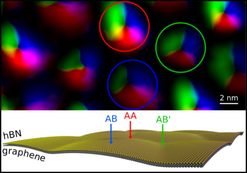
In this work we demonstrate that a free-standing van der Waals heterostructure, usually regarded as a flat object, can exhibit an intrinsic buckled atomic structure resulting from the interaction between two layers with a small lattice mismatch. We studied a freely suspended membrane of well-aligned graphene on a hexagonal boron nitride (hBN) monolayer by transmission electron microscopy (TEM) and scanning TEM (STEM). We developed a detection method in the STEM that is capable of recording the direction of the scattered electron beam and that is extremely sensitive to the local stacking of atoms. A comparison between experimental data and simulated models shows that the heterostructure effectively bends in the out-of-plane direction, producing an undulated structure having a periodicity that matches the moiré wavelength. We attribute this rippling to the interlayer interaction and also show how this affects the intralayer strain in each layer.
Keywords: van der Waals heterostructures, graphene, hexagonal boron nitride, scanning transmission electron microscopy
Boosted by the growing family of two-dimensional (2D) crystals, the study of van der Waals heterostructures1 has emerged in the last couple of years as one of the most active fields of research in the science of 2D materials. The interest in these materials can be explained by the practically infinite combinations of elementary monolayers that can be artificially stacked to create structures with desired properties. Among heterostructures, graphene on hexagonal boron nitride (hBN) is one of the most studied. Both crystals are chemically inert and have the same crystal structure, and their lattice constants only differ by 1.8%, making them an ideal match. Compared to SiO2, hBN provides a flatter, cleaner, and electronically more homogeneous insulating substrate2−4 and is now routinely used to manufacture high-performance devices.2,5,6 Besides serving as an excellent substrate, hBN also provides graphene with a periodical potential that, in the case of carefully aligned crystals, can lead to small commensurate areas.7
In contrast to previous works, where thick (bulk) hBN was used as a substrate for single-layer graphene, we investigate here a freely suspended heterostructure consisting of monolayer graphene on monolayer hBN. Since the sample does not have a rigid support, fundamental phenomena governing the interaction between the two crystals can be accessible in the absence of external perturbations. The structure is investigated via transmission electron microscopy (TEM) and scanning transmission electron microscopy (STEM), using low electron energies (80 keV for TEM and 60 keV for STEM) in order to minimize radiation damage.8 In our STEM investigation, we use a detection scheme that is very sensitive to small local tilts of the sample, which allows us to obtain the 3D shape of the heterostructure through a comparison to model structures.
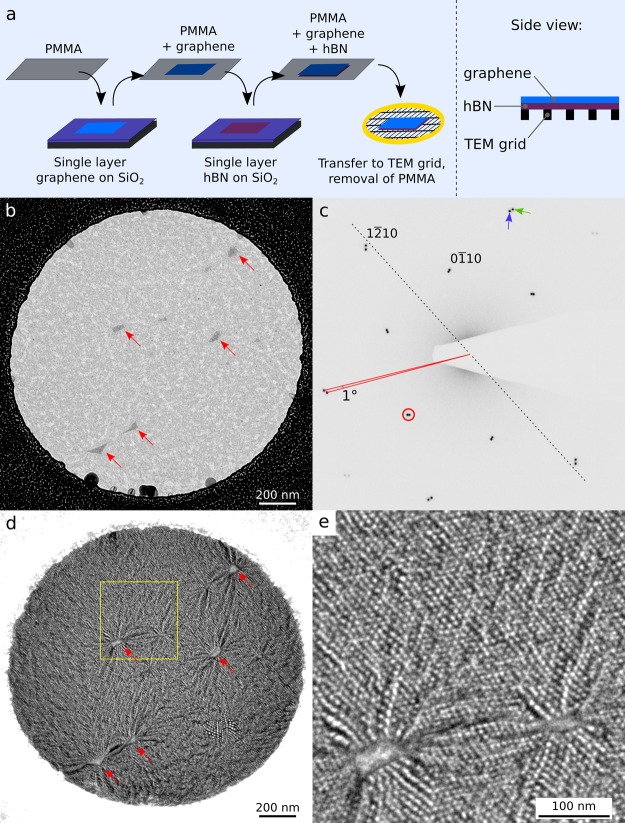
To fabricate the sample we started with a freshly cleaved hBN crystal on top of an oxidized Si wafer. A single layer hBN flake, chosen by direct optical observation, was picked up by a single layer graphene attached to a PMMA membrane following the method described in ref (9) and illustrated graphically in Figure 1a. The dry transfer method ensures an extremely clean interface between the flakes. Because both hBN and graphene cleave preferentially along their main crystallographic directions, during the transfer procedure we used flakes with well-defined facets and aligned them (within a precision of 1.5°) using a rotating positioning stage under an optical microscope. The resulting bilayer was then transferred onto a gold Quantifoil(R) TEM grid, where portions of the heterostructure are freely suspended on holes measuring approximately 1.5 μm in diameter (see side view in Figure 1a). A thin layer of Pt was deposited on the TEM grids (prior to attaching the 2D sample) in order to reduce hydrocarbon contamination.10
Figure 1.
CTEM analysis. The sample preparation and its transfer to the TEM grid are schematically described in panel a. (b) Bright field image of the heterostructure freely suspended on a hole in the Quantifoil(R) TEM grid. The red arrows indicate some aggregations of contaminants. (c) Electron diffraction pattern of the heterostructure from the suspended area in panel b. The green and the blue arrows indicate one graphene and one hBN diffraction spot, respectively. The misalignment between the two crystals is 1°. With reference to dark field imaging (d), the red circle marks the position of the objective aperture, and the dotted line indicates the tilt axis. (d) Dark field image of the same area as in panel b, acquired with a sample tilt of 16°. The red arrows point to the same features as in panel b. At these locations the moiré interference pattern is completely suppressed. (e) Magnified dark field image of the area inside the yellow square in panel d.
The heterostructure was first investigated in a conventional TEM (Philips CM200) operated at room temperature at 80 kV. Figure 1b shows a bright field (BF) image of the freely suspended heterostructure. At the locations marked with red arrows, dark patches of dirt are clearly visible. Their nature and position on the sample are discussed below. Figure 1c shows the electron diffraction pattern obtained by illuminating the whole suspended area of the sample. Two distinct sets of diffraction spots with hexagonal symmetry and 1° relative angular rotation can be observed. Because of the mismatch between the lattice constants of graphene and hBN (1.8%, with hBN being the larger of the two), it is possible to assign the outer and the inner set of spots to the graphene and to the hBN lattice, respectively. The green and the blue arrow in Figure 1c indicate one graphene and one hBN diffraction spot, respectively. The combination of lattice mismatch and relative rotation is expected to produce a moiré superlattice as already observed by AFM and STM in other works for the case of graphene on bulk hBN.3,4,7,11−13 The moiré interference pattern can be conveniently visualized in the TEM: Figure 1d shows a dark field (DF) image of the same area of Figure 1b, acquired with a sample tilt of 16°. Figure 1e shows the area inside the yellow square in Figure 1d at higher magnification. The tilt axis in the reciprocal space is indicated by the dotted black line in Figure 1c, and the objective aperture used for DF imaging is marked by a red circle. Note that the objective aperture was large enough to contain both one graphene and one hBN spot. In contrast to the BF image, here a strong modulation of the intensity appears, with bright spots arranged in a triangular lattice. The periodicity of this modulation is 9.8 nm, very close to the predicted moiré period of 9.9 nm for a 1° misaligned graphene/hBN bilayer.14 Interestingly, at some locations the moiré interference pattern is completely suppressed (marked by arrows, corresponding to the same locations marked in Figure 1b). We interpret these regions (which also appear much darker in the BF image) as pockets of contamination trapped between the layers, as reported previously on the basis of cross-sectional TEM imaging.15 At these locations, the two layers are effectively separated by amorphous contamination, and the diffraction conditions for moiré interference are suppressed. Indeed, the presence of the moiré in the DF-TEM images indicates that most of the graphene/hBN interface is atomically clean. Therefore, the clearly visible homogeneously distributed contamination, similar to what is typically seen in TEM studies of graphene, must be on the outer surfaces of the heterostructure.
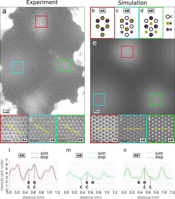
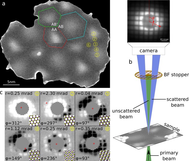
Further investigation on this sample was performed in a Nion UltraSTEM 100 operated at 60 kV. Figure 2a shows an atomically resolved medium angle annular dark field (MAADF) image of a small portion of the suspended heterostructure. In the range of scattering angles used here (ca. 60–200 mrad), regions where the atoms are precisely on top of each other appear brighter because the intensity here is not simply the sum of the two overlaid lattices, as it would be in a high angle annular dark field (HAADF) image.16 Indeed, in HAADF imaging (ca. 80–240 mrad), the intensity does not vary across the differently stacked regions (see Supplementary Figure 1). For this reason, and also because the MAADF image has a better signal-to-noise ratio than the HAADF image, MAADF imaging was preferred over HAADF in this work. There are three types of high-symmetry stacked regions labeled as AA (C atoms aligned with B and N atoms), AB (C atoms aligned with B atoms only), and AB′ (C atoms aligned with N atoms only). The top view structure models of the three stacking types are schematically shown in Figure 2b–d. In Figure 2f–h the AA, AB, and AB′ regions are shown at higher magnification in red, cyan, and green frames, respectively. A STEM simulation of the heterostructure, performed using the QSTEM software,17 is shown in Figure 2e, and the AA, AB, and AB′ regions are shown at higher magnification in Figure 2i–k. Figure 2l–n shows the intensity profiles for each of the three regions along the yellow lines of Figure 2f–k for the experimental (solid line) and for the simulated (dashed line) case. The AA region can be identified already from its visual appearance, which is distinctly different from that of the AB and AB′ regions (compare Figure 2f,i with Figure 2g,h,j,k). The AB and AB′ region can be distinguished by comparing the intensity modulation in the lattice, which is always stronger in the AB′ region (where C and N are aligned, Figure 2n) than in the AB region (where C and B are aligned, Figure 2m). Hence, from the appearance and relative intensity variations (Figure 2l–n are plotted with the same intensity scale), it is possible to unambiguously associate each moiré spot to a specific stacking type. After careful analysis of many regions across the sample, we observed that the AB stacked regions consistently appear larger than the AA and AB′ regions. This can be clearly seen for instance in Figure 3a, where a MAADF image containing several moiré spots is presented (a black mask was used here to cover contaminated areas). The three different moiré regions were identified as explained above for Figure 2. Individual AA, AB, and AB′ regions are enclosed by red, cyan, and green polygons, respectively. The sides of the polygons are placed approximately along the lines of minimum intensity between two adjacent moiré regions. Already at a first glance, it is evident that the AB region is the largest of the three. Indeed, as drawn in Figure 3a, the AB region measures 55 nm2, while the AA region is 34 nm2 and the AB′ region is 32 nm2.
Figure 2.
MAADF imaging. (a) Atomically resolved MAADF image of a portion of the heterostructure. Because of the contrast mechanism for medium angle scattering, high-symmetry regions appear brighter. The top-view structure models of the high-symmetry regions are shown in panels b–d. The regions in the colored squares of panel a are shown at higher magnification in panels f–h. (e) STEM MAADF simulation of the considered heterostructure. (i–k) Magnified views of the three high-symmetry regions of (e). (l–n) Gray value intensity profiles for the experimental (solid lines) and the simulated (dashed lines) case along the yellow lines in f–k. Scale bars in panels f–k are all 0.5 nm.
Figure 3.
(a) MAADF image of an area of the sample containing several moiré regions. The AB stacked region (enclosed in the cyan polygon) is found to be consistently larger than the AA (in red) and the AB′ (in green) regions. (b) Schematics of the experimental setup used for direction sensitive detection of the scattered electrons, including an example exposure recorded by the CCD camera and the polar coordinate system used to describe the position of the ACOM. (c) From the indicated regions (1–6) in panel a, the scattering intensity distributions are shown as the difference between a 10 × 10 pixels area binned signal and a reference signal that is obtained as an average of all recorded images (excluding those corresponding to contamination). Insets illustrate the local relative lattice offsets that are associated with the asymmetric scattering intensity. The red cross indicates the position of the ACOM in each image (the radial coordinate was exaggerated by a factor of 20). The r and φ coordinates of the ACOM position are also indicated for each image.
To get more insight into the local atomic stacking and to ultimately understand the reason behind the different sizes of the three moiré regions, we modified the detection mode of the STEM to extract information on the preferential scattering direction of the electron beam after interaction with the sample. A schematic drawing of the experimental setup is shown in Figure 3b. We used a charge-coupled device (CCD) camera to record a two-dimensional image of the scattered electron beam at every probe position during scanning, in a conceptually similar way as reported in refs (18−20) with the substantial difference that the DF signal instead of the BF disk was recorded in this experiment. The very intense bright field disk was shielded using a custom-made aperture consisting of a copper disk placed on a conventional 3 mm TEM grid (see Supporting Information for more details on the custom aperture). An example of such an image is shown in the upper part of Figure 3b. The relation between recorded image, preferential scattering direction, and local atomic stacking is based on the following argument: for high-symmetry stacked regions, i.e., at the center of AA, AB, and AB′ spots, the heterostructure shows perfect in-plane isotropy, and the electron beam will be elastically scattered along a cone around the axis of the primary beam. The corresponding image will therefore show symmetric illumination with respect to its center. However, when the probe hits the side of a moiré spot, where the two lattices are slightly off register, the electrons experience an anisotropic potential that results in the beam being predominantly scattered in one direction. Consequently, the recorded image will show asymmetric illumination. Examples of the locally obtained scattering intensity distributions are shown in Figure 3c, for selected points as drawn on the MAADF image of Figure 3a. The six images show important differences: regions 1 and 5, respectively centered on the AA and on the AB stacked regions, produce strong isotropic scattering of the beam around the center of the detector, with the AA region being the stronger scatterer of the two (as can also be seen from MAADF images). Regions 2 and 4 are respectively selected slightly off the centers of AA and AB spots, and in the corresponding scattering images the intensity is preferentially accumulated on one side of the detector. Finally, the center of mass of the detected intensity for regions 3 and 6 is at the center of the image, but the signal shows a two- and three-lobe geometry that mirrors the local symmetry of the corresponding regions. Since this signal is very sensitive to the local (projected) stacking of the two layers at each position, the comparison to simulated data from model structures allows us to establish the 3D structure of the free-standing bilayer heterostructure.
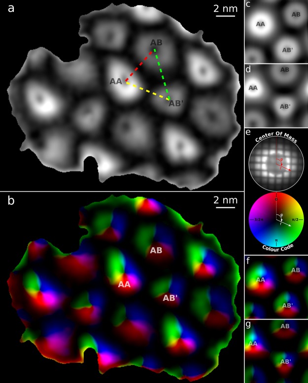
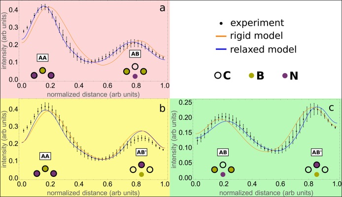
To quantitatively evaluate the preferential scattering direction, we take the diffracted intensity in the annular dark field pattern and measure its center of mass (annular center of mass, abbreviated as ACOM in the following) for each pixel of the scan. A representation in polar coordinates (r and φ) is used as schematically illustrated in Figure 3b. Examples of the calculated r and φ values of the scattered intensities for the six considered regions are noted in Figure 3c. Here, the position of the ACOM is also indicated by a red cross in each image, showing that only for regions 2 and 5 the ACOM is significantly displaced from the center of the detector. Figure 4a shows a map of the same sample region of Figure 3a obtained by assigning to each pixel the r value of the ACOM of the corresponding diffracted intensity encoded by a gray scale, where black and white colors correspond, respectively, to r = 0 and r = rmax. As expected from the considerations above, the map shows minima at the center of the moiré spots, indicating perfect symmetry, and maxima around these points, where the stacking offset produces prevalent electron scattering in one direction. Note that points halfway between two adjacent moiré spots are also dark. This is because in these regions the atomic stacking is perfectly halfway between two high-symmetry configurations and the coordinate r of the ACOM goes to zero (see regions 3 and 6 of Figure 3c). Figure 4b includes information on the angular direction of the preferential scattering, where the coordinate φ of the ACOM is encoded by the color (see Figure 4e for graphical explanation of the color code). It is interesting to observe how the scattering direction depends on the angle around the center of a moiré spot, spanning a range of 2π around each. For comparison, we performed STEM simulations based on a structure model consisting of a flat, rigid graphene/hBN heterostructure. Saving the simulated exit waves (ronchigrams) for each pixel allows us to treat the computed data set in the same way as its experimental counterpart. Figure 4c and f shows the results of this simulation. The experimental and the simulated maps show a qualitative agreement, but important differences become evident when comparing the relative sizes of the moiré spots. The black dotted lines in Figure 5a, b, and c are calculated by averaging 7–12 intensity profiles of Figure 4a along straight paths connecting adjacent moiré spot centers. Three such paths are indicated in Figure 4a by colored dashed lines, and they connect AA to AB (red), AA to AB′ (yellow), and AB to AB′ (green). The position of the minimum in each of these plots, which marks the transition between two adjacent stacking types, is significantly different for the experiment and the simulation based on the rigid model (orange solid lines). This disagreement can only be corrected by considering a new structural model for the simulation that allows for in-plane strain of the two crystals and/or out-of-plane distortion of the heterostructure. The flat and rigid graphene/hBN model has therefore to be abandoned in search of a more realistic atomic structure.
Figure 4.
Directional scattering analysis. (a) Radial (r) map of the ACOM of the same area of Figure 3a. The gray scale ranges from black (r = 0) to white (r = rmax). (b) Radial and angular (r + φ) map of the ACOM of the same area in (a). The color of each pixel is assigned based on the position of the ACOM by a one-to-one correspondence that is graphically explained in panel e. (c) Simulated r map and (f) r + φ map of the ACOM based on the rigid model. (d) Simulated r map and (g) r + φ map of the ACOM based on the relaxed model. Note that translations and rotations of the maps must be allowed when comparing them to each other.
Figure 5.
Intensity profiles of the radial maps of Figure 4 along paths connecting AA to AB (a), AA to AB′ (b), and AB to AB′ (c). The black dotted lines are the experimental profiles (obtained by averaging 7–12 individual profiles of Figure 4a); the orange lines are the simulated profiles of the rigid model (Figure 4c), and the blue lines are the simulated profiles of the relaxed model (Figure 4d).
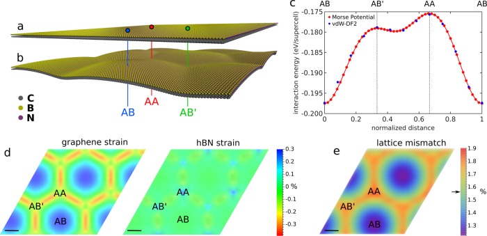
To this end we computed a relaxed graphene/hBN model by energy minimization using a combination of density functional theory (DFT) calculations and empirical potentials as explained in the following. Note that the combination of the two methods is a key point here, since full-scale DFT would be computationally prohibitive for a moiré unit cell consisting of ∼16 000 atoms, while empirical potentials have not been reported so far for the case of graphene on hBN. In order to determine the energy landscape of graphene on a hBN monolayer we followed the same approach as in ref (21) where several DFT methods for simulating the van der Waals interaction between the two layers were examined. For this work, the vdW-DF2 method22,23 was preferred over the computationally expensive many-body adiabatic fluctuation–dissipation theorem method24 and the DFT-D2 method, which accounts for long-range interactions through the addition of a semiempirical term.25 A supercell consisting of eight atoms (four carbon, two boron, and two nitrogen atoms) was constructed, and we calculated the interaction energy between the two layers defined as EvdW = E∞ – Ed0, where E∞ and Ed0 are the total energies of the supercell at infinite and at the equilibrium interlayer distances, respectively. The blue dots of Figure 6c show the calculated values of EvdW for the three high-symmetry stacking types and for other intermediate disregistry configurations. The plot clearly shows that the AB type is by far the most energetically favorable stacking type, followed by AB′ and finally by AA. This result is in agreement with existing literature21,26 (note that in ref (21) the AB and AB′ structures were inadvertently misidentified, with their names exchanged). To extend the calculation to the entire moiré unit cell, we now describe the van der Waals interaction between the layers by a Morse potential in the form V(r) = De(e–2α(r–re) – 2e–α(r–re)), where De is the value of the potential at the equilibrium interlayer distance re and α sets the width of the potential. The numerical values of the parameters were adjusted so that the interlayer interaction agrees with the DFT results, leading to DeCB = 2.9 meV, αCB = 2.08 Å–1, and re = 3.86 Å for the C–B interaction and to DeCN = 8.3 meV, αCN = 2.54 Å–1, and re = 3.84 Å for the C–N interaction. With these values, an excellent match could be obtained as shown by the red dots in Figure 6c. The C–C and B–N interaction is treated using many-body lcbop27 and Tersoff28,29 potentials, respectively, leading to a lattice mismatch of ∼1.6%. Both potentials are implemented in the code large-scale atomic/molecular massively parallel simulator (LAMMPS).30,31 For a moiré unit cell of graphene on hBN (0° misalignment), 65 × 65 unit cells of graphene on 64 × 64 unit cells of hBN are needed to keep the periodic boundary conditions, totaling 16 642 atoms. The structure with one degree of rotational misalignment is avoided as one would need to consider millions of atoms to properly model that structure. The total potential energy is minimized by relaxing both layers without applying any constraint until the forces are below 1.0 × 10⁻⁶ eV/Å.
Figure 6.
Results of calculations. (a) Rigid structure model of the graphene/hBN bilayer before relaxation. (b) Structure model of the graphene/hBN bilayer after full relaxation. The relaxed model visibly distorts in the out-of-plane direction. (c) Interlayer interaction energy plot per supercell (four carbon, two boron, and two nitrogen atoms). The blue dots represent the values obtained by DFT calculations for different stacking configurations, while the red dots indicate the shape of the Morse potential, whose parameters were optimized to fit to the DFT points. (d) In-plane strain maps of graphene (left) and hBN (right). (e) Lattice mismatch map. The black arrow next to the color bar indicates the initial lattice mismatch between the two crystals before the relaxation. Scale bars in panels d and e are 2 nm.
The initial and the fully relaxed models are presented in Figure 6a and b, respectively, with the three stacking types marked. The relaxed model visibly distorts in the out-of-plane direction, forming a wavy structure with a periodicity that matches the moiré superlattice. In particular, the AB region is found at a smooth bulge having the concavity on the graphene side, while at AA and AB′ regions the structure has sharper kinks with the concavity facing the hBN side. The total amplitude of the corrugation is ∼8.5 Å for each layer. The results of our relaxation are in good agreement with the theoretical prediction of ref.32
STEM simulations based on the relaxed model were performed, and the resulting r and r + φ maps are shown in Figure 4d and g, respectively. Although the rippling changes the positions of the moiré spots, the distances and relative angles between them do not change. Rather the main change to the moiré introduced by the rippling is the size and shape of the spots. In particular the rippling expands the AB region and causes the AA and AB′ regions to become more triangular, in much better agreement with the experiment. The intensity profiles for the map of the relaxed structure are shown in Figure 5a–c as blue solid lines. In Figure 5a and c the experimental and the simulated data based on the relaxed model now show excellent agreement, with both central minima being accurately reproduced. In other words, the plots from AA to AB (Figure 5a) and from AB to AB′ (Figure 5c) allow us to clearly distinguish the rigid, flat model from the relaxed, rippled structure. Along the line from AA to AB′ (Figure 5b), no significant difference between the flat and rippled model can be identified. This is not surprising because there is neither significant out-of-plane deformation nor in-plane lattice distortion (discussed further below) along this particular line in the relaxed structure. We also note that, while the positions of the maxima and minima in the profiles for the experiment and the simulation now match extremely well, the maximum amplitudes of the r values still deviate slightly (in Figure 5b and c the simulations slightly underestimate the amplitude near AA and AB, while they are overestimated near AB′). This cannot be due to inaccuracies in the structure model, because distortions in the membrane shape and layer alignment would shift the positions of maxima and minima, but not affect their amplitude. Nonlinearities of the detector, aberrations in the electron optics between sample and detector, or remaining inaccuracies in modeling of the scattering might be the reason. It is important to point out that none of these effects would affect the locations of the minima in r, since the minima reflect special cases in the symmetry of the projected structure. At this point, we will also comment briefly on how the ACOM analysis would compare to analyzing the MAADF intensity: each of the ACOM profiles as discussed above features two maxima and three minima, making the position of the central minimum very sensitive to the transition point between adjacent stacking types. A profile through the MAADF intensity, on the other hand, only has two side maxima with a single broad central minimum, which makes it very difficult to distinguish tiny differences in the stacking transition.
The superior match between the experiment and the relaxed rippled model indicates it is far more realistic than the flat model. We therefore compute the strain maps for the two layers in the relaxed structure. As shown in Figure 6d, the interatomic distances for both graphene and hBN are not constant but modulated with a periodicity matching the moiré wavelength. In particular, graphene tends to stretch at AB regions and compress along lines connecting AA to AB′ regions, while hBN appears mostly unstrained, with small local stretching accumulated at AA and AB′ regions. From the strain distribution in each layer we extract the lattice mismatch as shown in the map of Figure 6e. Here it can be clearly seen how the two layers attempt to minimize the mismatch at the AB regions, while at AA and AB′ the mismatch is significantly larger. This behavior can be explained by taking into account two conflicting effects, as already discussed in ref (7). As we demonstrated, AB is the most energetically favorable stacking type and the two crystals will attempt, by a combination of stretching and compression in each layer, to extend laterally this favorite stacking and thus to gain in van der Waals energy, at the expense of the AA and AB′ regions that will necessarily shrink. This behavior is in contrast to the elastic energy of the crystals’ lattices, which scales with the square of the strain and therefore attempts to restore the intrinsic lattice constants. The equilibrium is reached when these two competing forces cancel out. Note that the smallest value of lattice mismatch is ∼1.2%, indicating that the two lattices are never found in a completely synchronous state.
In conclusion, we have presented here a TEM study of a free-standing 2D van der Waals heterostructure consisting of a well-aligned bilayer of graphene on hBN. Dark field imaging in a conventional TEM confirms that the contaminants trapped between the two layers are squeezed into a few isolated pockets, leaving most of the heterostructure with an atomically clean interface. A direction sensitive acquisition mode for the scattered electron beam of a STEM was developed and employed to extract in-depth information on the local atomic stacking. The comparison with STEM simulations based on a relaxed model indicates that the heterostructure corrugates in the out-of-plane direction, with an undulation having the same periodicity as the moiré pattern and a total amplitude (in each layer) of ∼8.5 Å. This work shows that, depending on lattice mismatch and stacking misorientation, suspended heterostructures, usually regarded as pure 2D materials, should be effectively considered as 3D objects, with van der Waals interlayer forces playing a key role in determining the in-plane strain and out-of-plane deformation of each layer.
Acknowledgments
G.A., A.M., C.M., C.K., and J.C.M. acknowledge funding from the European Research Council (ERC) Project No. 336453-PICOMAT. M.R.A.M. and J.C.M. acknowledge financial support from the FWF Project No. P25721-N20. J.K. acknowledges funding from the Wiener Wissenschafts- Forschungs- und Technologiefonds (WWTF) via project MA14-009. T.J.P. acknowledges funding from the European Union’s Horizon 2020 research and innovation programme under the Marie Skłodowska-Curie grant agreement no. 655760 - DIGIPHASE. Computational resources from the Vienna Scientific Cluster are gratefully acknowledged. A.K.G. acknowledges funding from the European Research Council (ERC) project ARTIMATTER.
Supporting Information Available
The Supporting Information is available free of charge on the ACS Publications website at DOI: 10.1021/acs.nanolett.6b04360.
A comparison between MAADF and HAADF imaging, additional information on the custom aperture, as well as details on the STEM simulations (PDF)
The authors declare no competing financial interest.
Supplementary Material
References
- Geim A. K.; Grigorieva I. V. Nature 2013, 499, 419–25. 10.1038/nature12385. [DOI] [PubMed] [Google Scholar]
- Dean C. R.; Young A. F.; Meric I.; Lee C.; Wang L.; Sorgenfrei S.; Watanabe K.; Taniguchi T.; Kim P.; Shepard K. L.; Hone J. Nat. Nanotechnol. 2010, 5, 722–726. 10.1038/nnano.2010.172. [DOI] [PubMed] [Google Scholar]
- Decker R.; Wang Y.; Brar V. W.; Regan W.; Tsai H.-Z.; Wu Q.; Gannett W.; Zettl A.; Crommie M. F. Nano Lett. 2011, 11, 2291–5. 10.1021/nl2005115. [DOI] [PubMed] [Google Scholar]
- Xue J.; Sanchez-Yamagishi J.; Bulmash D.; Jacquod P.; Deshpande A.; Watanabe K.; Taniguchi T.; Jarillo-Herrero P.; LeRoy B. J. Nat. Mater. 2011, 10, 282–5. 10.1038/nmat2968. [DOI] [PubMed] [Google Scholar]
- Gannett W.; Regan W.; Watanabe K.; Taniguchi T.; Crommie M. F.; Zettl A. Appl. Phys. Lett. 2011, 98, 242105. 10.1063/1.3599708. [DOI] [Google Scholar]
- Kim E.; Yu T.; Song E. S.; Yu B. Appl. Phys. Lett. 2011, 98, 262103. 10.1063/1.3604012. [DOI] [Google Scholar]
- Woods C. R.; et al. Nat. Phys. 2014, 10, 451–456. 10.1038/nphys2954. [DOI] [Google Scholar]
- Susi T.; Hofer C.; Argentero G.; Leuthner G. T.; Pennycook T. J.; Mangler C.; Meyer J. C.; Kotakoski J. Nat. Commun. 2016, 7, 13040. 10.1038/ncomms13040. [DOI] [PMC free article] [PubMed] [Google Scholar]
- Kretinin A. V.; et al. Nano Lett. 2014, 14, 3270–3276. 10.1021/nl5006542. [DOI] [PubMed] [Google Scholar]
- Longchamp J.-N.; Escher C.; Fink H.-W. J. Vac. Sci. Technol., B: Nanotechnol. Microelectron.: Mater., Process., Meas., Phenom. 2013, 31, 020605. 10.1116/1.4793746. [DOI] [Google Scholar]
- Yankowitz M.; Xue J.; Cormode D.; Sanchez-Yamagishi J. D.; Watanabe K.; Taniguchi T.; Jarillo-Herrero P.; Jacquod P.; LeRoy B. J. Nat. Phys. 2012, 8, 382–386. 10.1038/nphys2272. [DOI] [Google Scholar]
- Tang S.; Wang H.; Zhang Y.; Li A.; Xie H.; Liu X.; Liu L.; Li T.; Huang F.; Xie X.; Jiang M. Sci. Rep. 2013, 3, 2666. 10.1038/srep02666. [DOI] [PMC free article] [PubMed] [Google Scholar]
- Wang D.; et al. Phys. Rev. Lett. 2016, 116, 126101. 10.1103/PhysRevLett.116.126101. [DOI] [PubMed] [Google Scholar]
- Hermann K. J. Phys.: Condens. Matter 2012, 24, 314210. 10.1088/0953-8984/24/31/314210. [DOI] [PubMed] [Google Scholar]
- Haigh S. J.; Gholinia A.; Jalil R.; Romani S.; Britnell L.; Elias D. C.; Novoselov K. S.; Ponomarenko L. A.; Geim A. K.; Gorbachev R. Nat. Mater. 2012, 11, 9–12. 10.1038/nmat3386. [DOI] [PubMed] [Google Scholar]
- Pennycook S. J.; Nellist P. D.. Scanning Transmission Electron Microscopy: Imaging and Analysis; Springer, 2011. [DOI] [PubMed] [Google Scholar]
- Koch C. T.Determination of core structure periodicity and point defect density along dislocations. Ph.D. thesis, 2002. [Google Scholar]
- Pennycook T. J.; Lupini A. R.; Yang H.; Murfitt M. F.; Jones L.; Nellist P. D. Ultramicroscopy 2015, 151, 160–167. 10.1016/j.ultramic.2014.09.013. [DOI] [PubMed] [Google Scholar]
- Müller-Caspary K.; Krause F. F.; Grieb T.; Löffler S.; Schowalter M.; Béché A.; Galioit V.; Marquardt D.; Zweck J.; Schattschneider P.; Verbeeck J.; Rosenauer A.. Ultramicroscopy 2016, 10.1016/j.ultramic.2016.05.004. [DOI] [PubMed] [Google Scholar]
- Ophus C.; et al. Nat. Commun. 2016, 7, 10719. 10.1038/ncomms10719. [DOI] [PMC free article] [PubMed] [Google Scholar]
- Zhou S.; Han J.; Dai S.; Sun J.; Srolovitz D. J. Phys. Rev. B: Condens. Matter Mater. Phys. 2015, 92, 155438. 10.1103/PhysRevB.92.155438. [DOI] [Google Scholar]
- Klimes J.; Bowler D. R.; Michaelides A. Phys. Rev. B: Condens. Matter Mater. Phys. 2011, 83, 195131. 10.1103/PhysRevB.83.195131. [DOI] [Google Scholar]
- Thonhauser T.; Cooper V. R.; Li S.; Puzder A.; Hyldgaard P.; Langreth D. C. Phys. Rev. B: Condens. Matter Mater. Phys. 2007, 76, 125112. 10.1103/PhysRevB.76.125112. [DOI] [Google Scholar]
- Harl J.; Schimka L.; Kresse G. Phys. Rev. B: Condens. Matter Mater. Phys. 2010, 81, 115126. 10.1103/PhysRevB.81.115126. [DOI] [Google Scholar]
- Grimme S. J. Comput. Chem. 2006, 27, 1787–1799. 10.1002/jcc.20495. [DOI] [PubMed] [Google Scholar]
- Sachs B.; Wehling T. O.; Katsnelson M. I.; Lichtenstein A. I. Phys. Rev. B: Condens. Matter Mater. Phys. 2011, 84, 195414. 10.1103/PhysRevB.84.195414. [DOI] [Google Scholar]
- Los J. H.; Fasolino a. Phys. Rev. B: Condens. Matter Mater. Phys. 2003, 68, 24107. 10.1103/PhysRevB.68.024107. [DOI] [Google Scholar]
- Tersoff J. Phys. Rev. B: Condens. Matter Mater. Phys. 1988, 37, 12. 10.1103/PhysRevB.37.6991. [DOI] [PubMed] [Google Scholar]
- Tersoff J. Phys. Rev. B 1989, 39, 8. [DOI] [PubMed] [Google Scholar]
- Plimpton S. J. Comput. Phys. 1995, 117, 1–19. 10.1006/jcph.1995.1039. [DOI] [Google Scholar]
- Plimpton S. J.; Thompson A. P. MRS Bull. 2012, 37, 513–521. 10.1557/mrs.2012.96. [DOI] [Google Scholar]
- Leven I.; Maaravi T.; Azuri I.; Kronik L.; Hod O. J. Chem. Theory Comput. 2016, 12, 2896–2905. 10.1021/acs.jctc.6b00147. [DOI] [PubMed] [Google Scholar]
Associated Data
This section collects any data citations, data availability statements, or supplementary materials included in this article.


