Abstract
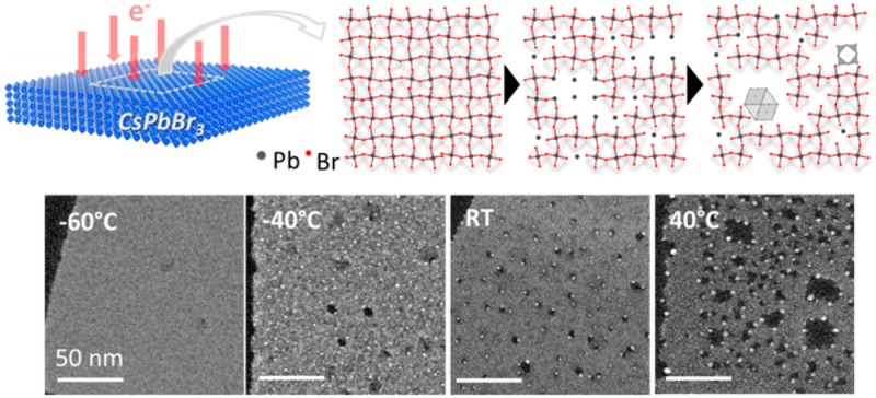
An increasing number of studies have recently reported the rapid degradation of hybrid and all-inorganic lead halide perovskite nanocrystals under electron beam irradiation in the transmission electron microscope, with the formation of nanometer size, high contrast particles. The nature of these nanoparticles and the involved transformations in the perovskite nanocrystals are still a matter of debate. Herein, we have studied the effects of high energy (80/200 keV) electron irradiation on colloidal cesium lead bromide (CsPbBr3) nanocrystals with different shapes and sizes, especially 3 nm thick nanosheets, a morphology that facilitated the analysis of the various ongoing processes. Our results show that the CsPbBr3 nanocrystals undergo a radiolysis process, with electron stimulated desorption of a fraction of bromine atoms and the reduction of a fraction of Pb2+ ions to Pb0. Subsequently Pb0 atoms diffuse and aggregate, giving rise to the high contrast particles, as previously reported by various groups. The diffusion is facilitated by both high temperature and electron beam irradiation. The early stage Pb nanoparticles are epitaxially bound to the parent CsPbBr3 lattice, and evolve into nonepitaxially bound Pb crystals upon further irradiation, leading to local amorphization and consequent dismantling of the CsPbBr3 lattice. The comparison among CsPbBr3 nanocrystals with various shapes and sizes evidences that the damage is particularly pronounced at the corners and edges of the surface, due to a lower diffusion barrier for Pb0 on the surface than inside the crystal and the presence of a larger fraction of under-coordinated atoms.
Keywords: cesium lead halide nanocrystals, TEM, radiation damage
Lead halide perovskites, both hybrid and all-inorganic, with general formula APbX3 (with A+ = CH3NH3+/NH2CH=NH2+/Cs+, and X– = Cl–/Br–/I–), have remarkable electronic properties1 that make them promising for applications in photovoltaics2 and optoelectronics.3−5 Compared to their bulk counterparts, APbX3 nanocrystals (NCs) have one or more dimensions that are reduced to a few to tens of nanometers, and their size and morphology can be manipulated to tune their optical properties.6,7 However, since surfaces and interfaces play important roles in material degradation,8,9 perovskite NCs may be inherently more unstable under irradiation by several sources (laser light, X-rays, electrons), heating, or exposure to moisture, than the corresponding bulk crystals.6−10 Such instability represents a major limitation for the widespread application of halide perovskite NCs in devices.
Recent transmission electron microscopy (TEM) studies of lead halide perovskite NCs (CH3NH3PbX3,10,11 (C4H9NH3)2PbBr4,12 and CsPbX313−17) have consistently reported the appearance of few nanometer size high contrast particles upon irradiation. Some of these reports indicated that the particles are made of metallic lead,11,13,16,17 a claim that is supported by the evidence that Pb2+ species from various material systems can be reduced to Pb0 by irradiation with electrons18 or with X-rays.8,19 Other studies of irradiation of APbX3 NCs have suggested that PbBr211 is also formed. Such discrepancies among the various reports underline an incomplete understanding of the overall transformations in the perovskite NCs, and especially of those leading to these high contrast particles. Compared to halide perovskites, the behavior of other materials systems under electron beam irradiation is better understood. For example, previous studies on oxides and on CaF2 have shown that their irradiation by an electron beam can induce the nucleation of metal particles and surface metallization.20−24 One typical case is the transformation of PbO2 to Pb through an intermediate PbO phase.18 It is known that the nucleation of metal particles and the surface metallization on oxides or on CaF2 occur in parallel with electron stimulated desorption processes through electronic excitation: in practice, while the cations are reduced to their metallic states, the anions (i.e., oxygen ions in oxides or fluoride ions in CaF2) are oxidized to neutral or even to positive species, which readily desorb from the surface.21,25−27 Stimulated desorption processes also occur under other types of irradiation, for example by photons.25
Here we demonstrate that high energy (80/200 keV) electron irradiation of APbX3 (CsPbX3 in the present case) NCs in a TEM causes the desorption of halogen species and the nucleation of metallic Pb particles. Also, by a temperature dependent study we were able to provide several details of the mechanism by which the Pb nanoparticles are formed. Our analysis was carried out on colloidal NCs having different shapes (cubes, wires, sheets), although it was mainly focused on CsPbBr3 nanosheets with 3 nm thickness and hundreds of nm width, a morphology that allows the observation of multiple events under identical irradiation conditions. We could identify two main stages in the transformation: (i) electron stimulated desorption of Br atoms and concomitant reduction of Pb2+ to Pb0, and (ii) diffusion of Pb0 atoms and their aggregation into Pb nanoparticles, with local amorphization and severe dismantling of the CsPbBr3 NCs. This process is more pronounced at lower electron energy, higher electron dose, and higher temperature, and is favored in higher surface-to-volume ratio NCs.
Results and Discussion
Knock-on damage and radiolysis are the two major electron-specimen interactions operative in an electron microscope with an incident electron energy of tens or hundreds of kiloelectron volt (keV).28 Knock-on damage involves an irreversible displacement of the nuclei in the specimen, when the transferred energy overcomes the displacement energy of the atoms in the material, and it is dominant at high energy.26,28,29 Ionization damage (or radiolysis) involves inelastic scattering, and is dominant at low energy.28,29 In the present case, for a better comprehension of the electron-specimen interaction we evaluated the evolution of halide perovskite NCs, which involved appreciable compositional change, upon electron beam irradiation at two different values of incident electron energy (E0) (see Figure S1). In particular, we verified that 80 keV electrons cause more effective damage (in terms of loss of Br atoms) than 200 keV electrons, suggesting that radiolysis rather than knock-on is the major mechanism of damage, as expected for both covalent and ionic crystals.29 Therefore, a thorough analysis of the compositional change of the perovskite NCs upon irradiation was carried out at E0 = 80 keV from areas containing thin nanosheets (3 nm thick, prepared as reported in our previous work14) at room temperature (RT), by acquiring energy-dispersive X-ray spectroscopy (EDS) spectra at regular time intervals up to a total accumulated dose of 6.5 × 10⁴ e–/Å2. Note that the starting 3 nm thick nanosheets were Cs-deficient (Cs1–xPbBr3, Figure S1), while the thicker crystals (for example, > 10 nm thick nanosheets) had the expected CsPbBr3 stoichiometry. However, for the sake of simplicity, the stoichiometric formula (CsPbBr3) will be used to address also the 3 nm thick nanosheets throughout this work.
Figure 1(a) reports EDS spectra (in the energy range of interest) at increasing doses from scanning TEM (STEM)-EDS analysis. Compositional changes were plotted by measuring the net peak intensity (proportional to the number of atoms) of the three elements of interest (Figure 1(b)). Upon irradiation, Cs and Pb intensities did not change appreciably, while the signal from Br decreased, especially at higher electron dose. This was also evident in the EDS elemental maps acquired at the boundary regions between areas exposed to different electron doses (see Figure S2). Note that an initial Br:Pb ratio lower than the stoichiometric one (3:1) was most likely caused by electron induced Br loss as soon as the EDS measurement was started. Such loss of Br atoms is analogous to the electron stimulated desorption of fluorine in CaF2, or of oxygen in several oxides, as said before.26 In the case of CaF2, F– is oxidized to F0 or to F+, and likewise in oxides O2– is oxidized to O0 or to O+. The neutral species (F0 or O0) diffuse and are desorbed due to their low reactivity. When positively charged species are formed, the Madelung potential is repulsive, and such species would be desorbed quickly when they are close to the surface.26 In our samples (and as already reported by others12−15), in parallel with the Br loss, high contrast particles were formed during electron beam irradiation on CsPbBr3 (orthorhombic phase, ICSD 97851), and these were identified as metal Pb nanoparticles with face centered cubic structure (ICSD 96501, see high-resolution TEM (HRTEM) image in Figure 1(c)).
Figure 1.
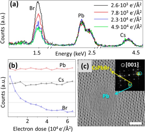
Br desorption and Pb nanoparticle formation during electron irradiation of 3 nm thick CsPbBr3 nanosheets at RT. (a) EDS spectra in the energy range of interest at increasing electron doses (E0 = 80 keV); (b) Plot of the net integrated peak intensity for Cs, Pb, and Br as a function of the electron dose from STEM-EDS analysis (E0 = 80 keV); (c) HRTEM of a Pb nanoparticle formed on CsPbBr3 nanosheet, with both CsPbBr3 and Pb oriented along the [001] zone axis (Scale bar: 2 nm, E0 = 200 keV, dose: 1140 e–/Å2), and (inset) Fast Fourier Transform (FFT) with the spots for CsPbBr3 {220} and Pb {200} circled.
We can therefore state that such transformations are due to electron stimulated desorption of Br and reduction of Pb2+ to Pb0. From Figure 1(a), the maximum fractional loss of Br was close to 2/3. Assuming that all the Pb2+ ions were reduced at the maximum loss of Br, we infer that the reduction of one Pb2+ ion was accompanied by the loss of two Br atoms, and this implies that a considerable fraction of Br– ions was very likely oxidized to Br0, and also that such oxidized species could diffuse and were ultimately desorbed from the NCs. A similar process was found to affect CsPbX3 NCs with different halogens (X=Cl, I) and even Cs4PbBr6 NCs (Figure S3). Details on the syntheses of these nanocrystals are found in the Supporting Information (SI). We also found that even irradiation by X-rays, by using the X-ray source of a X-ray photoelectron spectrometer (XPS), can cause a slight reduction of Pb2+ and a slight desorption of Br (see Figure S4). Therefore, our results and the observation of the Pb0 peak in recent XPS studies of organic lead halide perovskites8,30 imply that the Br desorption (and Pb2+ reduction) can be triggered by different types of radiation and can be generally classified as a stimulated desorption process. On the other hand, under irradiation by UV laser light lead halide perovskite NCs may undergo degradation via a different mechanism, as reported by Wang et al.(31)
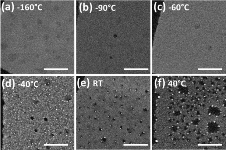
As mentioned above, the damage of CsPbBr3 nanosheets was slower at higher incident electron energy (E0 = 200 keV), hence this condition was chosen to capture the details of the following stage of evolution. Our experiments clearly show that Pb0 atoms aggregated to form Pb nanoparticles at a rate that depended on the temperature (see high angle annular dark field (HAADF)-STEM images in Figure 2). At low temperatures (i.e., −60 °C or lower), Br atoms were desorbed (Figure S1(b,c)) and Pb2+ ions were most likely reduced to Pb0, according to the electron-stimulated desorption mechanism described above. However, no Pb nanoparticles were visible (see Figure 2(a−c) and their HRTEM images in Figure S5(a)). This result suggests that, at these temperatures, Pb0 atoms did not have enough energy to overcome the activation barrier for diffusion, which would have enabled them to cluster into Pb particles at the surface of the NCs. Still, in this temperature range one cannot exclude that clusters containing only a few atoms (Pb nanoclusters) were formed, but in that case they were simply not discernible in the images. At higher temperatures (i.e., −40 °C or above), and still under irradiation, Pb0 atoms (and probably also clusters of Pb atoms) could instead diffuse and coalesce into observable Pb nanoparticles23,32 (Figure 2(d–f) and Figure S5(b)). As a general trend, higher temperatures promoted the formation of larger Pb particles (compare for example Figures 2d–f).
Figure 2.
Effect of temperature on the nucleation and growth of Pb nanoparticles in 3 nm thick CsPbBr3 nanosheets, as shown in HAADF-STEM images (Scale bars: 50 nm, E0 = 200 keV, the total doses for acquiring all the images are approximately ∼1.0 × 10³ e–/Å2): (a) −160 °C; (b) −90 °C; (c) −60 °C; (d) −40 °C; (e) RT; (f) 40 °C.
A question arises on whether electron beam heating has an important effect here. This is certainly true in materials with poor thermal conductivity. The two parameters that play a pivotal role in electron beam heating are dose rate (proportional to the beam current) and incident electron energy (E0). In the high temperature conditions at which visible Pb nanoparticles are formed, a study on the dependence of Pb nanoparticle formation on the irradiation dose rate for 200 keV electrons is reported in Figure S6. It shows that, in the range between 8.5 × 10⁵ and 2.0 × 10⁸ e–/Å2/s, the increase of size of Pb nanoparticle with increasing dose rate is negligible. The dose rate used in typical HRTEM and STEM imaging is within this range. Nevertheless, a higher dose rate induces the production of larger Pb nanoparticles, as demonstrated in Figure S6. We also found that at low temperatures (−60 °C or lower, which were conditions that did not promote the formation of observable Pb nanoparticles), with the same dose rate (5.0 × 10⁶ e–/Å2/s) used in Figure 2 (a–c) not even electron irradiation with ten times higher doses could induce the appearance of Pb nanoparticles. This suggests that a significant temperature rise does not occur even under irradiation with much higher doses. These observations evidence that electron beam heating of CsPbBr3 has a negligible effect at our experimental conditions for E0 = 200 keV. 80 keV electrons would have a thermal effect that is approximately 1.6 times the one from 200 keV electrons, which is still negligible within the dose rate employed in this work (see a more detailed discussion in the SI). In two different irradiation experiments, carried out at the higher temperature side of our tested interval (−40 °C and RT, see Figure 2(d,e)), we counted the numbers of Pb0 atoms within the observed nanoparticles and found them comparable (∼5 × 10⁵ in total, the Methods section explains how the calculations were made). This suggests that, although the perovskite lattice collapses locally, the Pb0 species are not lost from the NCs, a result that goes hand in hand with the quantitative EDS results reported in Figure 1. Instead, they are mainly sequestered in the formation of the metallic clusters, if the temperature is high enough.
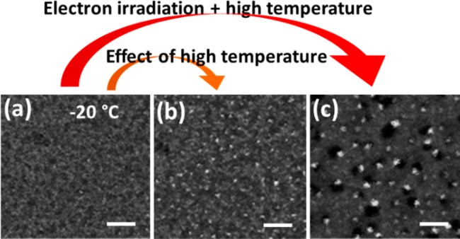
Both temperature and electron irradiation have a role in the nucleation and growth of Pb0 clusters. The effect of temperature has already been mentioned, and was made more evident by the control experiments reported in Figure 3. In this case, the sample was first irradiated at −20 °C, after which the temperature was raised (to RT). If, during this latter step, the electron beam was blanked (i.e., it was prevented to hit the sample), the initial, barely visible Pb nanoparticles that had formed at −20 °C evolved into larger particles (diameter ≤ 1.8 nm, an average value is hard to evaluate due to their small sizes), supporting the idea of temperature promoted diffusion of Pb0 species. If the temperature was raised while the sample was being irradiated, considerably larger Pb nanoparticles (2.3 ± 0.8 nm) were formed (see Figure 3). The electron induced heating is negligible at the used dose rate 8.5 × 10⁵ e–/Å2/s as discussed above and in Figure S6. It is likely that this occurred as the electron irradiation contributes to enhancing the diffusivity of Pb0 species and of small Pb nanoparticles by transferring momentum and energy to them.23,33 In addition, new Pb0 species were continuously generated by irradiation. This implies that, although the initial Br desorption and Pb2+ reduction is mainly due to a radiolysis process, we should also consider a contribution of knock-on displacement in the Pb nanoparticle nucleation process.
Figure 3.
HAADF-STEM images of 3 nm thick nanosheets (Scale bars: 20 nm, E0 = 200 keV): (a) Initially at −20 °C; (b) Following the acquisition of the image (a), the substrate temperature was raised to RT for 10 min with electron beam blanked, and again cooled to −20 °C for imaging of the same nanosheet; (c) image acquired at RT.
In the high temperature range, the Pb0 atoms can form the Pb nanoparticles by diffusing both along the surface and through the inner regions of the perovskite NCs, although diffusion from the bulk should be less marked in thicker samples. We compared the behavior of thin nanosheets (3 nm thick) with that of the thicker sheets (tens of nm thick) that were also present in the sample (note that the thicker sheets represented only a minor fraction of the sample). The comparison was quantified through compositional change under the same irradiation conditions. As shown in Figure S7, the Br concentration (at.%) dropped from 57% to 50% for 3 nm thick nanosheets, while it remained nearly constant at 59% for thicker nanosheets. The comparison evidenced that the thick nanosheets had undergone much less change and consequently less damage compared to the thin nanosheets (see Figure S7). This implies that both desorption of Br and aggregation of Pb0 species occur preferentially at the surface, which is expected since the surface is generally characterized by a lower barrier to atomic diffusion. Also, both Br and Pb atoms have lower coordination at the surface and their electronic configuration may be more easily altered by electron irradiation and additionally Br species are more easily desorbed when they are bound to surface sites than to inner regions of the sheets. As a consequence, the surface is energetically less stable than the bulk and plays an important role in the electron beam-induced degradation of perovskite NCs. Similar conclusions were drawn by Philippe et al.(8) and Yuan et al.(9) by exposing APbX3 thin films to different irradiations.
In addition to nanosheets, we also tested colloidal CsPbBr3 NCs with nanocuboid and nanowire shapes and different sizes, for which the syntheses are found in the Methods section. Overall, we found that the samples with higher surface-to-volume ratio (3 nm thick nanosheets, nanowires with diameters smaller than 10 nm, and nanocuboids with 8 nm edge) were more susceptible to electron irradiation than the samples with lower surface-to-volume ratio (see Figure 4, S7 and S8). The latter included: nanosheets that were tens of nm thick, nanowires wider than 10 nm, and cuboids with 20–40 nm edge (see Figures 4 and S7). In these larger NCs, the internal structure appeared to be preserved under irradiation, and only a few Pb nanoparticles were formed at their surface. On the other hand, lowering the incident electron energy to 80 keV could cause significant damage even to these NCs, due to the increased probability of inelastic interaction. An increase in temperature could also promote the process by speeding up the diffusion along the surface, as well as by promoting the diffusion from the inner regions of the NCs (above 60 °C), and this led to their fast degradation (see Figure S9). The dynamic evolution at high temperature for large nanocuboids is demonstrated in the Supporting Video S1. High surface-to-volume ratio NCs readily decomposed, which is clearly demonstrated in Figure 4. The 5 nm wide nanowires broke due to the formation of Pb nanoparticles. It is also remarkable that these Pb nanoparticles were rather regularly spaced along the wires. The nanocuboids with edge length of 8 nm decomposed by forming Pb nanoparticles at the corners (see Figure S8). A close investigation of Figure 4 revealed that edges and corners of the NCs are preferential sites for Pb particle formation.
Figure 4.
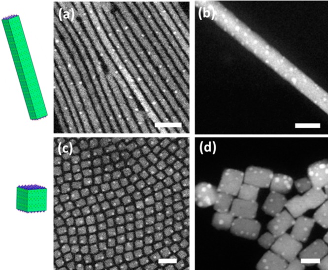
HAADF-STEM images showing preferential formation of Pb nanoparticles at the edges and corners of CsPbBr3 NCs: (a) 5 nm wide nanowires; (b) 20 nm wide nanowire; (c) nanocuboids with 8 nm edge; (d) nanocuboids with 20–40 nm edge (Scale bars: 20 nm, E0 = 200 keV, RT).
The starting sites of Pb reduction and Br desorption may be linked to defects. At a defect site, Pb ions may undergo reduction more easily. Starting preferentially from the defects, on 3 nm thick nanosheet voids with Pb nanoparticles on the edge are created. The formation of these Pb nanoparticles consumes part of the Pb from the surrounding perovskite lattice and leads to the formation of few small Pb nanoparticles at the surrounding locations. Overall, these processes result in the inhomogeneous damage in a single nanosheet (as can be seen in Figure 2 and Figure 3), even though the whole nanosheet is under homogeneous electron irradiation.
To monitor the formation of Pb nanoparticles at different sites under identical irradiation conditions, we took advantage of the large field of view of the direct electron detection camera combined with the large lateral size of the nanosheet to record them in a single HRTEM image (Figure 5(a)). Magnified views from the same image are displayed in Figure 5(b–f); i.e., all the events in these regions occurred simultaneously under the same irradiation conditions, which show as an eye-catching feature that the evolution of Pb nanoparticles at different sites is not synchronous. Some of the Pb nanoparticles exhibited a single-crystal structure, anisotropic shape (i.e., square/hexagonal projection) and well-defined orientation relationship (epitaxy) with the parent CsPbBr3 nanosheet (orthorhombic phase with ICSD: 97851, [001]-oriented on the support film). The relationships were: CsPbBr3 [001] ∥ Pb [001], CsPbBr3 (110) ∥ Pb (100), as shown for the particles in Figure 5(b,c) and for some of the particles of Figure 5(d,e). This suggests that the Pb atoms at the edge of these Pb nanoparticles may be bound to the parent CsPbBr3 lattice, and these are presumably early stage particles. Nonepitaxially bound, roughly spherical shapes were also found, such as the particles in Figure 5(e,f), including twinned NCs (particle P1). These nanoparticles may have resulted from a rearrangement of early stage Pb nanoparticles upon further irradiation. Our results support the idea that the epitaxial Pb particles bound to the surrounding parent lattice can survive until a critical size (i.e., number of Pb atoms). Above that size, the Pb atoms in the particle lose the epitaxial relationship with the surround lattice and rearrange, forming more isotropic particles which are thermodynamically more stable. This can be rationalized as due to two major reasons: (i) edge atoms are weakly bound to the surrounding lattice and the unstable bonds between the edge atoms and the surrounding lattice are broken due to the ongoing irradiation; and (ii) rearrangement results in the emergence of facets of lower energy. Among these more isotropic particles, some Pb nanocrystals exhibit twinning, a type of defect that is often seen in the case of metal nano- and microparticles, due to its low formation energy in metals.34 By feeding the Pb atoms to the surrounding Pb nanoparticles, some areas on the CsPbBr3 nanosheet turned into voids decorated by Pb nanoparticles at their edges (see Figure 5(e,f) and Figure 2(e,f)), while the Cs atoms as well as the remaining Pb and Br species were randomly distributed in the voids.
Figure 5.
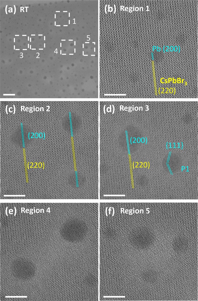
HRTEM analysis of Pb nanoparticle formation on a 3 nm thick CsPbBr3 nanosheet at RT: (a) Overview (Scale bar: 20 nm, E0 = 200 keV, total dose: 1140 e–/Å2); (b–f) Magnified view of five regions of interest in (a) (Scale bars: 5 nm).
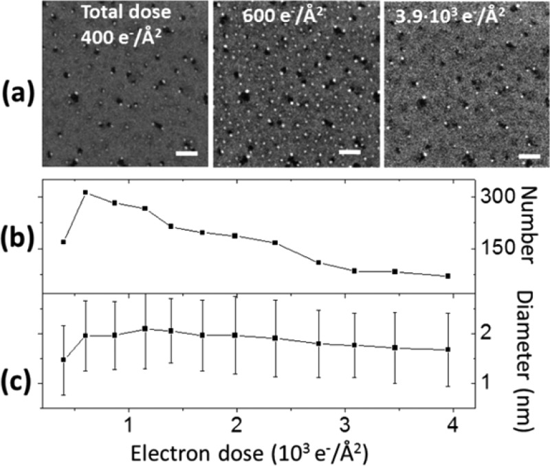
Once formed, the Pb nanoparticles were not stable under further electron irradiation. The evolution of the number and size distribution of the Pb nanoparticles is reported in Figure 6. At an electron dose of 400 e–/Å2, around 170 Pb nanoparticles had nucleated in the area shown in the HAADF-STEM image in Figure 6(a). This number rapidly increased to 310 at a dose of 600 e–/Å2 (Figure 6(a,b)). These nanoparticles were not stable and were dismantled under further electron irradiation: the number decreased to 70 at a dose of 3.9 × 10³ e–/Å2 (Figure 6(a,b)), and the particles basically disappeared at even higher doses. The same holds for Pb nanoparticles produced at different temperatures (see Figure S10). The size distribution of the Pb nanoparticles also changed during electron irradiation. For the Pb nanoparticles formed in Figure 6(a), the average size was 1.5 nm at a dose of 400 e–/Å2 and increased to 2.1 nm at a dose of 1.1 × 10³ e–/Å2. At a given temperature (i.e., surface diffusion rate), an equilibrium size was reached and did not increase any longer, and instead started to gradually decrease to 1.7 nm at a dose of 3.9 × 10³ e–/Å2.
Figure 6.
Evolution of number and size of Pb nanoparticles on 3 nm thick CsPbBr3 nanosheets at RT as a function of electron irradiation (E0 = 200 keV, RT). (a) HAADF-STEM images at four doses (Scale bars: 20 nm); (b) Number of Pb nanoparticles versus electron dose; (c) Average size of Pb nanoparticles versus electron dose (the diameter is calculated from the area by assuming a circular shape, error bar is the standard deviation).
The dominant reason for Pb particle size variation with increasing total dose is not heating. Note that, the slow variation of the average diameter of the Pb nanoparticles over time was due to the asynchronous evolution they underwent at different sites. According to our analysis based on the elemental maps of Figure S11, a Pb nanoparticle forms and then its size decreases under further electron irradiation, until the particle finally disappears. As the Pb composition recorded in the analyzed areas is constant (see the discussion for Figure 1) the dissolution of the Pb nanoparticle is unlikely to be the result of a sublimation or vaporization process. We also tend to exclude the participation of metallic Pb atoms in redox reactions under electron irradiation conditions, even though the surroundings of the Pb particles are chemically active. This is because, to do so, the metallic Pb atoms would have to stably lose electrons (i.e., be oxidized), which is unlikely when electrons are continuously supplied by irradiation.
The mechanism of dissolution of the Pb nanoparticles is revealed by the HRTEM study in Figure S12–S14. Following the amorphization of the Pb nanoparticles (Figure S12 and Figure S13), with further irradiation, Pb atoms spread out on the supporting film. In the case of 3 nm thick nanosheet, on which Pb nanoparticles decorate the edge of voids, the dissolution of Pb nanoparticles under further electron irradiation causes the decrease of the size of the voids, as observed in Figure 6. The dissolution of Pb nanoparticles from one isolated nanocuboid leads to continuous decomposition of the nanocuboid (Figure S13), while for an array of closely spaced nanocuboids the spread atoms accumulate at the regions between cuboids and appear as hollow frames that follow the initial contours of the cuboids (Figure S14). The atoms that have diffused from adjacent Pb nanoparticles could gather and form clusters (see Figure S15). This process is similar to the reported dissipation of Pd and Mo nanoparticles through diffusion under electron beam irradiation.35 Therefore, if we rule out the possibility of vaporization and redox reactions, the most probable mechanism for the “disappearance” of Pb nanoparticles under prolonged electron irradiation is through diffusion and spreading out of Pb atoms on the remaining perovskite lattice and on the carbon film of the TEM grid.
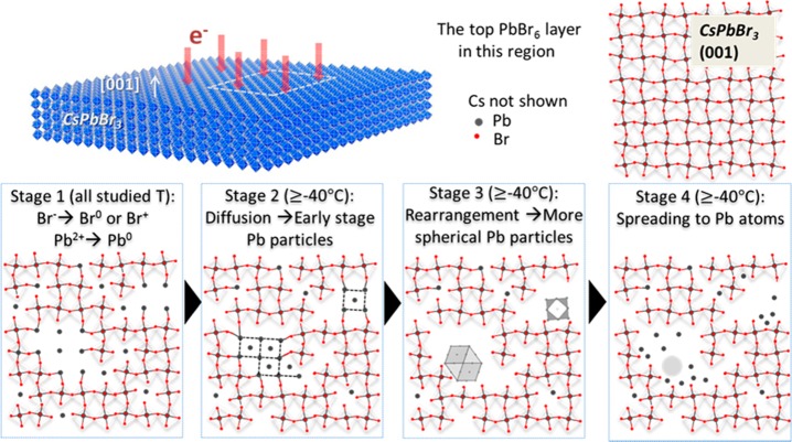
To summarize the above-presented results, the overall process of electron beam-induced transformations in CsPbBr3 NCs is schematically summarized in Figure 7. For demonstration purposes, we show the evolution of Pb nanoparticles in an irradiated area, and we draw only the topmost PbBr6 octahedron layer. Considering that, in the CsPbBr3 structure, mainly covalent bonds form between Pb and Br, and mainly ionic bonds form between Cs and Br, while Pb and Cs atoms are not bound to each other,36 the following stages can be identified on the basis of the above results:
Figure 7.
Schematics depicting the stages in the evolution of an irradiated area in a CsPbBr3 nanosheet ([001] orientation). Only the atomic model for the topmost layer of PbBr6 octahedra is shown for clarity.
Stage 1. The whole process starts with the oxidation of Br– and reduction of Pb2+ at all studied temperatures (Figures 1 and Figure S1), which is likely to occur preferentially at the corners and edges of the surface of the NC. Oxidized halide species desorb from the surface.
Stage 2. At high temperatures (above −40 °C), in tandem with electron induced motion (i.e., by momentum transfer), the reduced Pb0 atoms diffuse preferentially along the surface and aggregate into single-crystal Pb nanoparticles, which possess anisotropic shapes and epitaxial relationships with the parent nanosheet lattice, probably due to partial binding to the surrounding lattice. Note that a higher temperature (above 60 °C) can enable the diffusion of Pb0 also from the inner perovskite lattice.
Stage 3. The bonds between the early Pb nanoparticles and the parent CsPbBr3 NCs are broken upon further irradiation, hence the Pb nanoparticles evolve toward more isotropic shapes, giving rise to voids. The Pb particles are located at the boundary between the voids and the remaining perovskite lattice (as shown in Figures 2 and 6).
Stage 4. Upon further electron irradiation, the Pb nanoparticles amorphize, then they become smaller and finally fade as the Pb atoms spread on the remains of the CsPbBr3 surface or on the support film.
Conclusions
The experiments presented here demonstrate that the electron beam induced nucleation of Pb nanoparticles on CsPbX3 NCs is mainly due to a radiolysis damage process. Electron irradiation (80 keV/200 keV) induces the desorption of halogen atoms from the surface of the NCs and the reduction of Pb2+ to metallic Pb0, in analogy with the electron stimulated desorption mechanism reported in the literature. This process also occurs under other types of irradiation, such as X-rays. Subsequently, adjacent Pb0 atoms diffuse and aggregate into Pb nanoparticles at a temperature dependent rate, which is simultaneously aided by electron irradiation, most probably due to electron beam-induced motion via knock-on displacement of the Pb0 atoms on the surface. At temperatures high enough for diffusion to occur, on CsPbBr3 NCs, anisotropic Pb nanoparticles epitaxially oriented and bound to the parent structure are produced. These rearrange into more spherical particles under further irradiation, after the bonds between their edge atoms and the surrounding parent CsPbBr3 NCs are broken. The nucleated Pb nanoparticles are unstable and are dismantled under further electron irradiation. The formation of Pb nanoparticles preferentially occurs at the corners and edges of the surface of the NCs. In this context, CsPbBr3 NCs with higher surface-to-volume ratio are prone to decompose by electron beam-induced Pb nanoparticles formation, while lower surface-to-volume ratio CsPbBr3 NCs are more robust. We could also safely exclude any significant electron beam heating under our experimental conditions.
The mechanism presented in this study may also govern the formation of high contrast particles observed in TEM images of hybrid lead halide perovskite NCs,37 tin halide perovskite NCs,38 and other perovskite related materials such as CsPb2Br5,39 and it helps defining some precautions to follow. When dealing with halide perovskites characterization using electron microscopy, increasing the incident electron energy of the microscope can largely improve the stability of the sample. By lowering the substrate temperature, the characterization of high aspect ratio perovskite NCs becomes feasible as a consequence of the retarded decomposition process. Besides, radiation induced damage may be exploited for patterning purposes, i.e., by creating Br-rich and Br-deficient areas, or for selectively inducing anion exchange in different regions, to enable patterned luminescent surfaces, where each pixel in the display device should correspond to the whole irradiated area, in order to avoid the inhomogeneity caused by the electron beam. Besides, in principle the Pb formation process can be used to make porous perovskite NCs. These can be advantageous compared to nonporous perovskite NCs in sensing applications, because the analytes can penetrate into the pores and interact more strongly with the perovskite. Another potential application is to enable a cation exchange process with the aid of the Pb2+ reduction under electron irradiation to produce a shell of perovskite with another element on the surface, as a route toward fabricating core–shell perovskite NCs.
Methods
Electron Beam Irradiation in the TEM
The electron beam irradiation experiments were carried out in a 200 kV microscope (JEOL JEM-2200FS) equipped with a spherical aberration corrector (CEOS) for the objective lens and an in-column image filter (Ω-type). The acceleration voltage can be lowered to 80 kV by means of an electric short switch. The base pressure in the TEM column was 2 × 10⁻⁷ mbar.
High Resolution TEM (HRTEM)
The electron dose is reported for each HRTEM image. The images were acquired with two types of detectors: a CCD camera with 2048 × 2048 pixels (UltraScan 1000, Gatan Inc.), and a direct electron detection camera (K2 Summit, Gatan Inc.), with 7420 × 7676 pixels in super-resolution mode. The K2 camera is able to capture images on a large field of view with atomic resolution, while minimizing electron exposure. The HRTEM images were acquired with the K2 camera unless specified.
Probe Current Measurements
We first calibrated the electron counts on the CCD camera using the direct electron detection camera for which electron number is directly counted. Then the probe current was measured by acquiring the Scanning TEM (STEM) probe on UltraScan 1000. With a spot size of 1.5 nm and convergence semiangle of 16 mrad, the resulting probe current was 68 pA (corresponding to a current density of 3.8 × 10³ A/cm2) and was varied by selecting the spot size.
High Angle Annular Dark Field (HAADF-STEM) and Energy Dispersive X-ray Spectrometry (EDS) Analysis
A Bruker Quantax 400 EDS system with an XFlash 5060 detector was used for elemental analysis. The NCs composition was estimated from the EDS spectra in the thin film approximation (Cliff-Lorimer) by fitting the Cs Lα, Pb Lα and Br Kα lines, with a relative error of 10% for Cs, 10% for Pb, 4% for Br, evaluated as the standard deviation in the fit.
Temperature Dependent Study
A JEOL EM-21130 specimen heating holder with an electric furnace and EM-SHU2 heater control was used for observing the effect of higher temperatures on electron beam-induced transformations in CsPbBr3 nanocrystals. A Gatan cryotransfer holder with liquid nitrogen cooling equipped with a Model 900 Smartset cold stage controller was used for observing the electron beam-induced transformation at low temperatures.
X-ray Photoelectron Spectroscopy (XPS)
A Kratos Axis Ultra DLD spectrometer equipped with a monochromatic Al Kα source (photon energy = 1486.6 eV) was used for irradiation and characterization. Nanosheets were exposed to continuous X-ray exposure at a photon flux of 2.4 × 10¹¹ photons/mm2 s. High-resolution spectra were acquired with an analyzer pass energy of 10 eV and steps of 0.1 eV. The pressure in the chamber was kept below 10–8 mbar and the takeoff angle set at Φ = 0°. Energy calibration was performed fixing the C–C component of C 1s spectrum at 284.8 eV. Relative atomic percentages of different species were computed from high-resolution spectra, fitted with Voigt functions using CasaXPS software.
Synthesis of CsPbBr3 Nanocrystals
Thin, rectangular shaped nanosheets around 3 nm thick, with lateral size of several 100 nm up to few μm were synthesized by a colloidal procedure reported elsewhere.14 CsPbBr3 nanowires with rectangular cross section were synthesized by a colloidal procedure previously reported by us.15 CsPbBr3 nanocuboids with 8 nm edge were synthesized by a colloidal procedure similar to the one reported previously.6 The CsPbBr3 nanocuboids with edge length of 20–40 nm were synthesized following the same colloidal procedure as for CsPbBr3 nanoplatelets, except that ethanol was used in the place of acetone.13 The TEM samples were prepared by drop-casting 10 μL of the colloidal suspensions onto ultrathin carbon/holey carbon coated Cu grids.
Calculation of Pb0 Atoms in the Pb Nanoparticles
The total number of Pb0 atoms contained in Pb nanoparticles was estimated as follows: the total area of the Pb nanoparticles in the HAADF-STEM images was measured in ImageJ,40 and then the total volume of Pb nanoparticles was calculated and multiplied by the atomic density of crystalline Pb to give the total number of Pb0 atoms.
Acknowledgments
The authors acknowledge funding from the European Union under grant agreement no. 614897 (ERC Grant TRANS-NANO).
Supporting Information Available
The Supporting Information is available free of charge on the ACS Publications website at DOI: 10.1021/acsnano.6b08324.
EDS analysis of CsPbBr3 nanosheets, Pb nanoparticles formation on CsPbCl3 and CsPbI3, Pb2+ reduction under X-ray exposure, effect of temperature, electron beam heating, formation of Pb nanoparticles on CsPbBr3 NCs with different surface-to-volume ratios, instability of Pb nanoparticles with electron irradiation, syntheses of CsPbX3 (X=Cl, I) and Cs4PbBr6 NCs (PDF)
Video S1: The dynamic evolution at high temperature for large CsPbBr3 nanocuboids (AVI)
The authors declare no competing financial interest.
Supplementary Material
References
- Stoumpos C. C.; Kanatzidis M. G. The Renaissance of Halide Perovskites and Their Evolution as Emerging Semiconductors. Acc. Chem. Res. 2015, 48, 2791–2802. 10.1021/acs.accounts.5b00229. [DOI] [PubMed] [Google Scholar]
- Yang W. S.; Noh J. H.; Jeon N. J.; Kim Y. C.; Ryu S.; Seo J.; Seok S. I. High-Performance Photovoltaic Perovskite Layers Fabricated through Intramolecular Exchange. Science 2015, 348, 1234. 10.1126/science.aaa9272. [DOI] [PubMed] [Google Scholar]
- Song J.; Li J.; Li X.; Xu L.; Dong Y.; Zeng H. Quantum Dot Light-Emitting Diodes Based on Inorganic Perovskite Cesium Lead Halides (CsPbX3). Adv. Mater. 2015, 27, 7162–7167. 10.1002/adma.201502567. [DOI] [PubMed] [Google Scholar]
- Zhu H.; Fu Y.; Meng F.; Wu X.; Gong Z.; Ding Q.; Gustafsson M. V.; Trinh M. T.; Jin S.; Zhu X. Y. Lead Halide Perovskite Nanowire Lasers with Low Lasing Thresholds and High Quality Factors. Nat. Mater. 2015, 14, 636–642. 10.1038/nmat4271. [DOI] [PubMed] [Google Scholar]
- Stoumpos C. C.; Malliakas C. D.; Peters J. A.; Liu Z.; Sebastian M.; Im J.; Chasapis T. C.; Wibowo A. C.; Chung D. Y.; Freeman A. J.; Wessels B. W.; Kanatzidis M. G. Crystal Growth of the Perovskite Semiconductor CsPbBr3: A New Material for High-Energy Radiation Detection. Cryst. Growth Des. 2013, 13, 2722–2727. 10.1021/cg400645t. [DOI] [Google Scholar]
- Protesescu L.; Yakunin S.; Bodnarchuk M. I.; Krieg F.; Caputo R.; Hendon C. H.; Yang R. X.; Walsh A.; Kovalenko M. V. Nanocrystals of Cesium Lead Halide Perovskites (CsPbX3, X = Cl, Br, and I): Novel Optoelectronic Materials Showing Bright Emission with Wide Color Gamut. Nano Lett. 2015, 15, 3692–3696. 10.1021/nl5048779. [DOI] [PMC free article] [PubMed] [Google Scholar]
- Huang H.; Polavarapu L.; Sichert J. A.; Susha A. S.; Urban A. S.; Rogach A. L. Colloidal Lead Halide Perovskite Nanocrystals: Synthesis, Optical Properties and Applications. NPG Asia Mater. 2016, 8, e328. 10.1038/am.2016.167. [DOI] [Google Scholar]
- Philippe B.; Park B.-W.; Lindblad R.; Oscarsson J.; Ahmadi S.; Johansson E. M. J.; Rensmo H. Chemical and Electronic Structure Characterization of Lead Halide Perovskites and Stability Behavior under Different Exposures—a Photoelectron Spectroscopy Investigation. Chem. Mater. 2015, 27, 1720–1731. 10.1021/acs.chemmater.5b00348. [DOI] [Google Scholar]
- Yuan H.; Debroye E.; Janssen K.; Naiki H.; Steuwe C.; Lu G.; Moris M.; Orgiu E.; Uji-i H.; De Schryver F.; Samorì P.; Hofkens J.; Roeffaers M. Degradation of Methylammonium Lead Iodide Perovskite Structures through Light and Electron Beam Driven Ion Migration. J. Phys. Chem. Lett. 2016, 7, 561–566. 10.1021/acs.jpclett.5b02828. [DOI] [PMC free article] [PubMed] [Google Scholar]
- Zhu F.; Men L.; Guo Y.; Zhu Q.; Bhattacharjee U.; Goodwin P. M.; Petrich J. W.; Smith E. A.; Vela J. Shape Evolution and Single Particle Luminescence of Organometal Halide Perovskite Nanocrystals. ACS Nano 2015, 9, 2948–2959. 10.1021/nn507020s. [DOI] [PubMed] [Google Scholar]
- Sichert J. A.; Tong Y.; Mutz N.; Vollmer M.; Fischer S.; Milowska K. Z.; García Cortadella R.; Nickel B.; Cardenas-Daw C.; Stolarczyk J. K.; Urban A. S.; Feldmann J. Quantum Size Effect in Organometal Halide Perovskite Nanoplatelets. Nano Lett. 2015, 15, 6521–6527. 10.1021/acs.nanolett.5b02985. [DOI] [PubMed] [Google Scholar]
- Dou L.; Wong A. B.; Yu Y.; Lai M.; Kornienko N.; Eaton S. W.; Fu A.; Bischak C. G.; Ma J.; Ding T.; Ginsberg N. S.; Wang L.-W.; Alivisatos A. P.; Yang P. Atomically Thin Two-Dimensional Organic-Inorganic Hybrid Perovskites. Science 2015, 349, 1518–1521. 10.1126/science.aac7660. [DOI] [PubMed] [Google Scholar]
- Akkerman Q. A.; Motti S. G.; Srimath Kandada A. R.; Mosconi E.; D’Innocenzo V.; Bertoni G.; Marras S.; Kamino B. A.; Miranda L.; De Angelis F.; Petrozza A.; Prato M.; Manna L. Solution Synthesis Approach to Colloidal Cesium Lead Halide Perovskite Nanoplatelets with Monolayer-Level Thickness Control. J. Am. Chem. Soc. 2016, 138, 1010–1016. 10.1021/jacs.5b12124. [DOI] [PMC free article] [PubMed] [Google Scholar]
- Shamsi J.; Dang Z.; Bianchini P.; Canale C.; Stasio F. D.; Brescia R.; Prato M.; Manna L. Colloidal Synthesis of Quantum Confined Single Crystal CsPbBr3 Nanosheets with Lateral Size Control up to the Micrometer Range. J. Am. Chem. Soc. 2016, 138, 7240–7243. 10.1021/jacs.6b03166. [DOI] [PMC free article] [PubMed] [Google Scholar]
- Imran M.; Di Stasio F.; Dang Z.; Canale C.; Khan A. H.; Shamsi J.; Brescia R.; Prato M.; Manna L. Colloidal Synthesis of Strongly Fluorescent CsPbBr3 Nanowires with Width Tunable Down to the Quantum Confinement Regime. Chem. Mater. 2016, 28, 6450–6454. 10.1021/acs.chemmater.6b03081. [DOI] [PMC free article] [PubMed] [Google Scholar]
- Tong Y.; Bladt E.; Aygüler M. F.; Manzi A.; Milowska K. Z.; Hintermayr V. A.; Docampo P.; Bals S.; Urban A. S.; Polavarapu L.; Feldmann J. Highly Luminescent Cesium Lead Halide Perovskite Nanocrystals with Tunable Composition and Thickness by Ultrasonication. Angew. Chem., Int. Ed. 2016, 55, 13887–13892. 10.1002/anie.201605909. [DOI] [PubMed] [Google Scholar]
- Yu Y.; Zhang D.; Kisielowski C.; Dou L.; Kornienko N.; Bekenstein Y.; Wong A. B.; Alivisatos A. P.; Yang P. Atomic Resolution Imaging of Halide Perovskites. Nano Lett. 2016, 16, 7530–7535. 10.1021/acs.nanolett.6b03331. [DOI] [PubMed] [Google Scholar]
- Pan Z. W.; Dai Z. R.; Wang Z. L. Lead Oxide Nanobelts and Phase Transformation Induced by Electron Beam Irradiation. Appl. Phys. Lett. 2002, 80, 309–311. 10.1063/1.1432749. [DOI] [Google Scholar]
- Stanley H. B.; Banerjee D.; van Breemen L.; Ciston J.; Liebscher C. H.; Martis V.; Merino D. H.; Longo A.; Pattison P.; Peters G. W. M.; Portale G.; Sen S.; Bras W. X-Ray Irradiation Induced Reduction and Nanoclustering of Lead in Borosilicate Glass. CrystEngComm 2014, 16, 9331–9339. 10.1039/C4CE00937A. [DOI] [Google Scholar]
- Gnanavel T.; Möbus G. In-Situ Cobalt Nanocrystal Synthesis by Intense Electron Beams in Tem. J. Phys. Conf. Series 2012, 371, 012047. 10.1088/1742-6596/371/1/012047. [DOI] [Google Scholar]
- Sepulveda-Guzman S.; Elizondo-Villarreal N.; Ferrer D.; Torres-Castro A.; Gao X.; Zhou J. P.; Jose-Yacaman M. In Situ Formation of Bismuth Nanoparticles through Electron-Beam Irradiation in a Transmission Electron Microscope. Nanotechnology 2007, 18, 335604. 10.1088/0957-4484/18/33/335604. [DOI] [Google Scholar]
- Pereira W. d. S.; Andres J.; Gracia L.; San-Miguel M. A.; da Silva E. Z.; Longo E.; Longo V. M. Elucidating the Real-Time Ag Nanoparticle Growth on α-Ag2WO4 During Electron Beam Irradiation: Experimental Evidence and Theoretical Insights. Phys. Chem. Chem. Phys. 2015, 17, 5352–5359. 10.1039/C4CP05849F. [DOI] [PubMed] [Google Scholar]
- Tamou Y.; Tanaka S.-i. Formation and Coalescence of Tungsten Nanoparticles under Electron Beam Irradiation. Nanostruct. Mater. 1999, 12, 123–126. 10.1016/S0965-9773(99)00079-3. [DOI] [Google Scholar]
- Smith D. J.; McCartney M. R.; Bursill L. A. The Electron-Beam-Induced Reduction of Transition Metal Oxide Surfaces to Metallic Lower Oxides. Ultramicroscopy 1987, 23, 299–303. 10.1016/0304-3991(87)90239-7. [DOI] [Google Scholar]
- Knotek M. L. Stimulated Desorption. Rep. Prog. Phys. 1984, 47, 1499–1561. 10.1088/0034-4885/47/11/002. [DOI] [Google Scholar]
- Gonzalez-Martinez I. G.; Bachmatiuk A.; Bezugly V.; Kunstmann J.; Gemming T.; Liu Z.; Cuniberti G.; Rummeli M. H. Electron-Beam Induced Synthesis of Nanostructures: A Review. Nanoscale 2016, 8, 11340–11362. 10.1039/C6NR01941B. [DOI] [PubMed] [Google Scholar]
- El Mel A.-A.; Molina-Luna L.; Buffière M.; Tessier P.-Y.; Du K.; Choi C.-H.; Kleebe H.-J.; Konstantinidis S.; Bittencourt C.; Snyders R. Electron Beam Nanosculpting of Kirkendall Oxide Nanochannels. ACS Nano 2014, 8, 1854–1861. 10.1021/nn406328f. [DOI] [PubMed] [Google Scholar]
- Egerton R. F. Mechanisms of Radiation Damage in Beam-Sensitive Specimens, for Tem Accelerating Voltages between 10 and 300 Kv. Microsc. Res. Tech. 2012, 75, 1550–1556. 10.1002/jemt.22099. [DOI] [PubMed] [Google Scholar]
- Williams D. B.; Carter C. B.. Transmission Electron Microscopy: A Textbook for Materials Science; Springer: New York, 2009. [Google Scholar]
- Raga S. R.; Jung M.-C.; Lee M. V.; Leyden M. R.; Kato Y.; Qi Y. Influence of Air Annealing on High Efficiency Planar Structure Perovskite Solar Cells. Chem. Mater. 2015, 27, 1597–1603. 10.1021/cm5041997. [DOI] [Google Scholar]
- Wang Y.; Li X.; Sreejith S.; Cao F.; Wang Z.; Stuparu M. C.; Zeng H.; Sun H. Photon Driven Transformation of Cesium Lead Halide Perovskites from Few-Monolayer Nanoplatelets to Bulk Phase. Adv. Mater. 2016, 28, 10637–10643. 10.1002/adma.201604110. [DOI] [PubMed] [Google Scholar]
- Asoro M. A.; Kovar D.; Shao-Horn Y.; Allard L. F.; Ferreira P. J. Coalescence and Sintering of Pt Nanoparticles: In Situ Observation by Aberration-Corrected HAADF STEM. Nanotechnology 2010, 21, 025701. 10.1088/0957-4484/21/2/025701. [DOI] [PubMed] [Google Scholar]
- Egerton R. F. Beam-Induced Motion of Adatoms in the Transmission Electron Microscope. Microsc. Microanal. 2013, 19, 479–486. 10.1017/S1431927612014274. [DOI] [PubMed] [Google Scholar]
- Elechiguerra J. L.; Reyes-Gasga J.; Yacaman M. J. The Role of Twinning in Shape Evolution of Anisotropic Noble Metal Nanostructures. J. Mater. Chem. 2006, 16, 3906–3919. 10.1039/b607128g. [DOI] [Google Scholar]
- Tanaka M.; Takeguchi M.; Furuya K. Behavior of Metal Nanoparticles in the Electron Beam. Micron 2002, 33, 441–446. 10.1016/S0968-4328(01)00046-4. [DOI] [PubMed] [Google Scholar]
- Qian J.; Xu B.; Tian W. A Comprehensive Theoretical Study of Halide Perovskites ABX3. Org. Electron. 2016, 37, 61–73. 10.1016/j.orgel.2016.05.046. [DOI] [Google Scholar]
- Vybornyi O.; Yakunin S.; Kovalenko M. V. Polar-Solvent-Free Colloidal Synthesis of Highly Luminescent Alkylammonium Lead Halide Perovskite Nanocrystals. Nanoscale 2016, 8, 6278–6283. 10.1039/C5NR06890H. [DOI] [PubMed] [Google Scholar]
- Jellicoe T. C.; Richter J. M.; Glass H. F. J.; Tabachnyk M.; Brady R.; Dutton S. E.; Rao A.; Friend R. H.; Credgington D.; Greenham N. C.; Böhm M. L. Synthesis and Optical Properties of Lead-Free Cesium Tin Halide Perovskite Nanocrystals. J. Am. Chem. Soc. 2016, 138, 2941–2944. 10.1021/jacs.5b13470. [DOI] [PubMed] [Google Scholar]
- McLaughlan S. D.; Evans H. W. Production of Colloidal Calcium by Electron Irradiation of CaF2 Crystals. Phys. Status Solidi B 1968, 27, 695–700. 10.1002/pssb.19680270226. [DOI] [Google Scholar]
- Schneider C. A.; Rasband W. S.; Eliceiri K. W. Nih Image to Imagej: 25 Years of Image Analysis. Nat. Methods 2012, 9, 671–675. 10.1038/nmeth.2089. [DOI] [PMC free article] [PubMed] [Google Scholar]
Associated Data
This section collects any data citations, data availability statements, or supplementary materials included in this article.


