Abstract
A coupler is an indispensable component to sample the forward and reflected power for the real-time radio frequency (RF) power monitoring system. The directivity of a coupler is a critical factor to achieve accurate RF power measurements. This paper proposes a microstrip coupler with a tunable high directivity circuit to accurately measure the reflected RF power. The directivity tuner composed of passive components adjusts phase and amplitude of the coupled RF signal, and cancel out the leakage signal from the RF input port at the coupled reflection port. The experimental results, which agree with simulation results, show that the microstrip coupler with the directivity tuner circuit has a compact size (~ 0.07 λg x 0.05 λg), high power capability (up to 1 kW), and high directivities (more than 40 dB) at operating frequency bands (f = 297.3 MHz, 400 MHz, and 447 MHz, respectively) for magnetic resonance imaging (MRI) applications.
Index Terms: microstrip coupler, directivity, isolation, passive components, microstrip circuits, magnetic resonance imaging (MRI), RF power monitoring
I. INTRODUCTION
Real-time RF power monitoring is an essential part in modern wireless communication system to satisfy the minimum transmitting power requirement and to limit the reflected power by the impedance mismatch [1], [2]. An RF coupler is used to sample the RF power without significant loss or distortion of the main signal. It is a key device in RF power measurements. Among the characteristics of a coupler, the directivity, which is defined by the difference between coupling factor and isolation, plays a critical role to separate the transmitting signal in a main line and coupled reflection signal in a coupled line [1], [2]. Insufficient isolation causes the uncertainty of the results of RF reflected power measurements because transmitted high power affects the reflected power measurements [2]. To improve the directivity, some approaches include: modified patters of a pair of coupled lines, the insertion of passive components, and the utilization of active devices [3]–[12]. This paper proposes a compact microstrip coupler with the tunable high directivity circuit that controls phase and amplitude at the operating frequency band. The directivity tuner cancels out the forward leakage signal in a coupled line and an RF power meter that is connected at the coupled reflection port receives only reflected signal from the load port. The application of a tunable high directivity coupler proposed in this paper is RF power monitoring in magnetic resonance imaging (MRI) systems [13]. The aim is to design, fabricate, and test a high directivity coupler, which has approximate 25 dB to 30 dB coupling factor, compact size (less than 5 cm x 5 cm), high directivity (greater than 40 dB), and high power capability (up to 1 kW) at 297.2 MHz for 7-tesla (T), 400 MHz for 9.4 T, and 447 MHz for 10.5 T MRI scanners. Comparison results of simulation and experimentation with the conventional coupler are also included.
II. THEORY
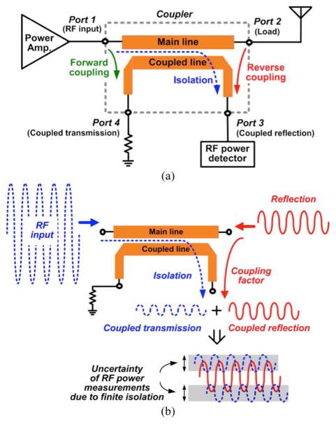
Fig. 1. (a) presents a schematic of a general RF power measurement with a microstrip coupler to monitor the reflected RF power. The RF power detector (e.g., conventional envelope, RMS, or logarithmic converting device from RF to dc output) connected to the port 3 should receive only a coupled reflection power (solid red line). However, a portion of RF input power in the port 1 appears at port 3 (dotted blue line) due to the finite isolation. In that case, a portion of the transmission power is added to the reflected power in the coupled line as shown in Fig 1(b), and thus the coupled reflection signal at the port 3 becomes inaccurate by a high standing wave ratio (SWR). In general, forward power is much larger than reflected power, and the influence of the reflected power is insignificant when the forward power measurement is performed as (1) shows the uncertainty of the forward power. However, forward high RF power can impact on the reflected power measurement, and it is difficult to accurately measure the reflected power without high directivity as given by (2) of the reflected power uncertainty [2].
Fig. 1.
Illustration of RF power measurement and its uncertainty of the output: (a) a general RF power monitor with a microstrip coupler in a wireless system and (b) its signal components and uncertainty in a reflected RF power measurement.
| (1) |
| (2) |
where IL is insertion loss, RL is return loss, and D is the directivity of a coupler in dB.
When a coupler is ideal, even- and odd- mode characteristic impedance (Zoe and Zoo) and phase constants (βe and βo) comply with (3). In this case, the RF input power does not affect the reflected RF power at the port 3 as given by (4).
| (3) |
| (4) |
However, most microstrip couplers are non-ideal, and the phase constants in even- and odd-mode are not equal (5), thus the isolation between the port 1 and the port 3 defined by (6) is no longer negligible [1].
| (5) |
| (6) |
where
The unequal phase constants are the main factors that generate finite isolation resulting in low directivity [14], [15].
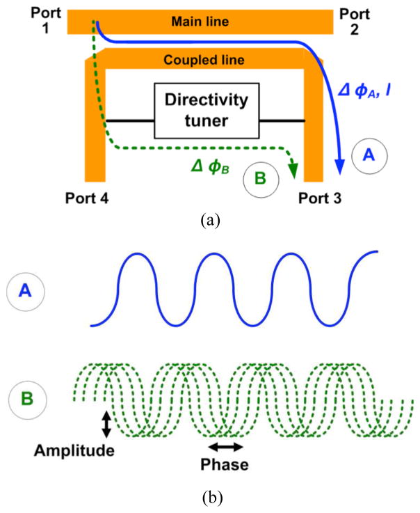
To compensate the unequal phase constants, the directivity tuner is proposed as shown in Fig. 2. The coupled forward signal is divided into signal A (solid line) on the coupled microstrip line and signal B (dotted line) through the directivity tuner. The phase and amplitude of signal B are controlled by the directivity tuner as shown in Fig. 2(b) and therefore the signal A is cancelled out by the signal B at the coupled reflection port (Port 3).
Fig. 2.
(a) A microstrip coupler with a proposed directivity tuner, and (b) two signal components through microstrip line, A, and directivity tuner, B, in (a)
The signal A is presented by the ABCD matrix (7), and the transmission and the phase shift of the signal A are defined by (8) and (9), respectively, when the lossless electrical model from the coupled line of the Port 1 to the Port 3 is considered to analyze and compare the signal A and signal B [16]–[18].
| (7) |
| (8) |
| (9) |
where θA = (βl)A is the electrical length, l is a physical length, and Zc is the characteristic impedance of the coupled microstrip line for the signal A.
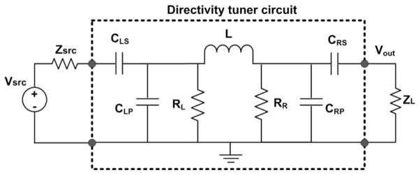
Fig. 3 shows the implementation of the directivity tuner with the Thevenin circuit model. The directivity tuner circuit is considered to analyze the behavior of the signal B and other parts (e.g., short microstrip lines for connections and parasitic losses) are ignored to simplify the electrical model. The ABCD matrix of the signal B is presented by (10), the transmission is defined by (11) when the Thevenin equivalent circuit model is applied as shown in Fig. 3, and the phase shift is defined by (12) [16]–[18]. In practical, when the loss term of the coupled line where the signal A flows is considered, the signal A and the signal B are completely cancelled out by the manipulation of the directivity tuner if ΔϕA = ΔϕB + π and the loss of the signal A is equal to the loss of signal B defined by (13). Thus, properly selected values of passive components in the directivity tuner circuits create high isolation (i.e., high directivity) at the target frequency.
Fig. 3.
Directivity tuner circuit with the Thevenin equivalent circuit model.
| (10) |
| (11) |
| (12) |
| (13) |
where s = j(2πfreq.), .
III. DIRECTIVITY TUNER
A proposed coupler with the directivity tuner has high power capability and low insertion loss because it uses a microstrip coupled line that does not include any component on the main signal line. The implementation with passive components enables a compact size of a high directivity coupler. In this section, design parameters and their effects to generate the high directivity resulting in reducing power measurement uncertainty are described. Tunable capability to meet the specifications of MRI applications and insensitivity to loading conditions by the tunability are also presented.
A. Design parameters
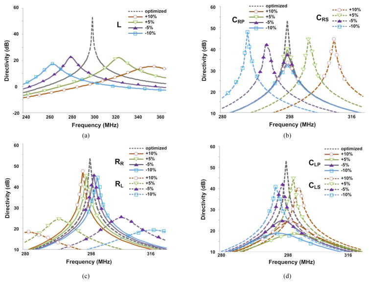
There are seven elements in the directivity tuner in Fig 3. The optimized passive component values to make high directivity of a coupler are defined by ADS simulation (Keysight Technology) to meet the target coupling-factor of 25 dB – 30 dB within a compact size of 5 cm x 5 cm. The directivity of 62.2 dB is achieved at 298 MHz for 7 T MRI scanner when the design parameters are optimized with L = 36 nH, CLS = 132 pF, CLP = 8.2 pF, RL = 97 Ω, RR = 54 Ω, CRP = 1 pF, and CRS = 24 pF with the coupled line of the length of 28 mm and the space of 0.2 mm. Fig. 4 shows the simulated directivity variations when the design parameters are swept from −10% to +10% from the optimized values to identify the impact of each element on the directivity of the coupler. The L, CRS, and RL dominantly change the operating frequency of the directivity tuner. The CRP and CLP mainly change the magnitude. The RR and CLS finely shift the peak of the directivity around the desired operating frequency.
Fig. 4.
Design parameters of the directivity tuner and simulated directivity variations using the design parameters sweep from −10% to +10% from the optimized values (L = 36 nH, CLS = 132 pF, CLP = 8.2 pF, RL = 97 Ω, RR = 54 Ω, CRP = 1 pF, and CRS = 24 pF). (a) L, (b) CRP and CRS, (c) RR and RL, and (d) CLP and CLS.
B. Tunable capability
The capacitances of CLS and CRP that have low impacts of the controllability as shown in Fig. 4 are fixed to reduce the complexity of tunable circuits. Although the L (inductor) has a high impact of the operating frequency on the directivity tuner, the inductance of L is fixed due to difficulties in making tunable inductor and adjusting the inductance. Fig. 5 shows simulation results of the tunable capability of the directivity tuner to cover ultra-high fields (7 T and beyond) in MRI application. When CRS = 12.5 pF, CLP = 5.2 pF, RL = 155 Ω, and RR = 101 Ω, the coupling factor (S32) of a coupler is 26 dB and the isolation (S31) is −104.3 dB, thus the directivity of 78.7 dB is achieved for 9.4 T. When CRS = 9.5 pF, CLP = 5 pF, RL = 173 Ω, and RR = 125 Ω, the coupling factor (S32) of a coupler is 25 dB and the isolation (S31) is −105.5 dB, thus the directivity of 80.5 dB is achieved for 10.5 T. The simulation results show the values are within the reasonable ranges of tunable passive components
Fig. 5.
Simulated tunability of the directivity tuner for ultra-high field MRI applications (7 T, 9.4 T, and 10.5 T).
C. Reducing power uncertainty
The Table 1 shows the comparison of the power uncertainty when the property of a conventional coupler (coupling factor = 25 dB and directivity = 25 dB) and the simulation results of the high directivity coupler in Fig. 5 are used. The error range of the high directivity coupler at the coupled reflection port (the port 3 in Fig. 1) is limited less than 1 %. The increased directivity values have greatly higher impact on the reflected RF power measurement than the forward power measurement. Therefore, a small load change can be detectable with the high directivity.
TABLE 1.
Comparison of the power uncertainty
| Coupling factor (dB) | Return loss (dB) | Isolation (dB) | Directivity (dB) | Max power uncertainty* (%) | |||
|---|---|---|---|---|---|---|---|
| Forward | Reflected | ||||||
| Conventional coupler | 25 | 25 | 45 | 25 | 3.9 | 35 | |
| High directivity coupler | 7 T | 24.8 | 39 | 87.3 | 62.5 | 0.05 | 0.43 |
| 9.4 T | 26 | 35.9 | 88 | 62 | 0.06 | 0.46 | |
| 10.5 T | 25 | 34.8 | 90.4 | 65.5 | 0.04 | 0.31 | |
Maximum reflected power uncertainty with VSWR = 2 at port 3
D. High power capability
The proposed coupler with the directivity tuner uses a coupled microstrip line, and there is no element on the main signal line from the input port to the load port that is connected to a resonating structure (e.g., antenna or RF coil in MRI). Thus, this structure has the benefits of the low insertion loss and high power capability. A strong-coupled coupler has not been considered in this study because of high power loss in a coupling structure [19]. The coupling factor in the coupled line can be selected according to the operating power level to prevent damage in the directivity tuner circuits. The high directivity coupler has been tested up to 1 kW RF power with the coupling factor close to 25 dB in a MRI application.
IV. EXPERIMENTAL RESULTS AND DISCUSSION
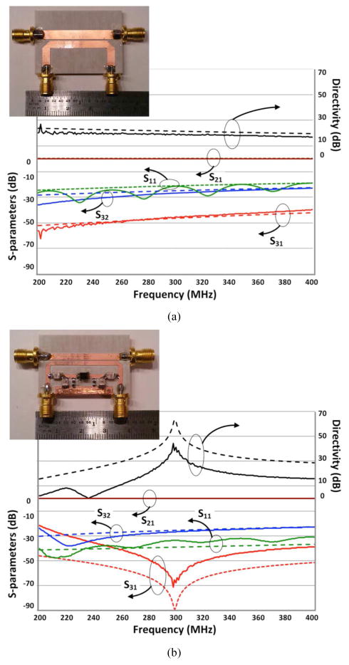
Fig. 6 shows the results of simulations (dotted line) and experiments (solid line) with the conventional coupler and the proposed high directivity coupler. They are fabricated on a dielectric substrate (Rogers RO4003, εr = 3.55). Lumped elements (i.e., capacitors, resistors, and inductors) for the directivity tuner circuit have non-magnetic properties that have been checked by the specification and magnet test. The proper values of the circuit to build high directivity (over 40 dB) are selected during experiments with a network analyzer (E8362B, Keysight Technology) after selecting coarse values by the simulation results as described in the previous section. The coupling factor (S32) and isolation (S31) were measured by using a network analyzer, and then the directivities were calculated. The port 4 is terminated to 50 Ω and the remaining ports were terminated to 50 Ω during coupling factor and isolation measurements. The conventional coupler and the high directivity coupler have the same coupling factor of 27 dB. The directivity of the conventional coupler is 18 dB, whereas the high directivity coupler has 45 dB at 298 MHz. Therefore, the maximum reflected power uncertainty decreases from 165.5% to 5.7% in case of VSWR = 1.5 by the well-adjusted directivity tuner. For example, the uncertainty of reflected power measurement is limited within 1.5 dBm (9.3 dBm to 7.8 dBm) when the coupler has a directivity of 45 dB, coupling factor of 27 dB, transmit power of 50 dBm, and VSWR of 1.5. However, the uncertainty is sharply increased to 3.2 dBm (13.3 dBm to 10.1 dBm) when the directivity decreases to 18 dB, and other characteristics remain the same. As seen in Fig. 6, the high directivity coupler has larger difference between the simulation and experimental result of isolation (S31) than difference of the conventional coupler. It shows that parasitic electrical and electromagnetic effects, mainly capacitive coupling, affect the tuner circuit and it is hard to compensate parasitic elements without finely adjusted values of the passive components.
Fig. 6.
Comparison of a conventional (a) and proposed high directivity coupler (b): fabricated couplers (left top), simulated (dotted lines) and measured (solid lines) S-parameters, and calculated directivity values, respectively.
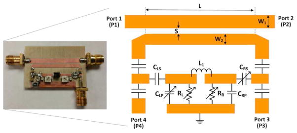
The high directivity coupler with tunable capability has been fabricated and tested as shown in Fig. 7 and Fig. 8. The Port 4 is internally terminated to 50 Ω and other ports are connected to SMA connectors. The design parameters are presented in Table 2. To validate the performance of the tunable high directivity coupler at each operating frequency region, S-parameters were measured and then the directivity was calculated as shown in Fig. 8. When measuring coupling factor and isolation, the remaining port was terminated to 50 Ω. The directivity of the tunable high directivity coupler has at least 40 dB over the operating frequencies by adjusting the combination of capacitors (tuning range: 40 pF) and resistors (tuning range: 200 Ω).
Fig. 7.
Photograph of the tunable high directivity coupler (left) and a schematic (right).
Fig. 8.
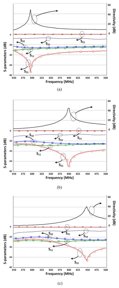
Measured S-parameters with the tunable high directivity coupler at (a) 298 MHz for 7 T, (b) 400 MHz for 9.4 T, and (c) 440 MHz for 10.5 T.
TABLE 2.
Design parameters of the tunable high directivity coupler
| CLS (pF) | CLP (pF) | RL (Ω) | L1 (nH) | RR (Ω) | CRP (pF) | CRS (pF) | Directivity (dB) | Max power uncertainty* (%) | ||
|---|---|---|---|---|---|---|---|---|---|---|
| Forward | Reflected | |||||||||
| 7 T | 100 | 7.5 | 160 | 35 | 50 | 1 | 20 | 48 | 0.27 | 2.4 |
| 9.4 T | 100 | 6 | 150 | 35 | 52 | 1 | 13 | 44 | 0.42 | 3.8 |
| 10.5 T | 100 | 1.2 | 85 | 35 | 55 | 1 | 8 | 41 | 0.6 | 5.4 |
L = 28 mm, S = 0.4 mm, W1 = 3 mm, W2 = 2.3 mm
Maximum reflected power uncertainty with VSWR = 2 at port 3
The results of this work are compared to other recently published microstrip couplers in Table 3. To our knowledge, there was no tunable coupler with high directivity (greater than 40 dB) and the relative physical size to the operating frequency is smaller than other couplers. Although the proposed coupler has very high directivity, the bandwidth is limited as expected. However, the MRI application of this microstrip coupler has a single operating frequency, and thus the limited bandwidth is unimportant. Alternatively, the high directivity circuit can be tunable by adjusting the directivity tuner.
TABLE 3.
Comparison between this work and recently published microstrip couplers.
| Design method | Coupling factor (dB) | Center frequency (MHz) | Normalized bandwidth* (%) | Directivity (dB) | Size** (λg) | Tunable capability | |
|---|---|---|---|---|---|---|---|
| This work at 7 T | Microstrip with lumped elements | 25 | 298 | 8.8 | 48.2 | 0.05 x 0.03 | Yes |
| This work at 9.4 T | 25 | 400 | 8 | 43.7 | 0.07 x 0.04 | Yes | |
| This work at 10.5 T | 25 | 440 | 7.8 | 41.2 | 0.07 x 0.05 | Yes | |
| [8] | Epsilon negative transmission line | 10 | 2000 | 8.7 | 40 | 0.4 x 0.27 | No |
| [9] | Double coupled lines with an unmatched load | 20 | 1500 | - | 40 | 0.07 x 0.08 | No |
| [10], (structure 1) | Microstrip with fragment structure | 20 | 2000 | 45 | 48 | 0.25 x 0.1 | No |
| [11] | Wiggly microstrip line | 20 | 2250 | 20 | 35 | 0.25 x 0.04 | No |
| [12] | Microstrip with shut inductors | 20 | 2400 | 16.3 | 56 | 0.25 x 0.21 | No |
Normalized bandwidth = fC/fBW, fc: center frequency, fBW: bandwidth of 20 dB directivity with less than 20 dB return loss
Normalized coupling structure size (λ0: the guide wavelength at the center frequency)
The directivity of a coupler is sensitive to loading conditions. When the port 2 in Fig. 2 deviates from the preset 50 Ω matching condition, the directivity sharply decreases. The conventional coupler in Fig. 4(a) and the high directivity coupler in Fig. 4(b) have been investigated to compare the sensitivity to loading conditions. As a result of the comparison, Fig. 9 shows the stable directivity of the coupler with the directivity tuner. This stable characteristic of the high directivity coupler provides the accurate reflected RF power that is proportional to loading conditions.
Fig. 9.
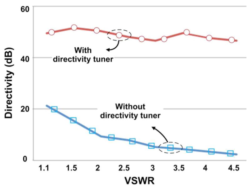
Experimental comparison of the load sensitivity of the directivity.
The low insertion loss of less than 0.2 dB, which is represented by S21, is an important parameter for high power transmitters or transceivers. A compact size is also valuable asset. Both were achieved in the high directivity microstrip coupler.
V. CONCLUSION
A microstrip coupler with an additional passive component circuit (i.e., the directivity tuner) has obtained a high directivity of greater than 45 dB, which is more than 25 dB improvement and insensitivity to loading changes compared to the result of a conventional coupler. Therefore, the high directivity coupler design significantly reduces the uncertainty of the reflected RF power measurement. This high directivity coupler can be tunable and cover ultra-high field (7 T and beyond) MRI applications with the high power capability and the compact size.
Acknowledgments
This study was supported by the following U.S National Institute of Health (NIH) grants: NIH-NIBIB-P41-EB015894 and NIH-NIBIB-R01-EB006835
This work was supported by NIH Grants P41 EB015894, K99EB020058, and R01 EB006835.
Biographies

Sung-Min Sohn (S’11-M’13) received the B.S. and M.S. degrees from Korea University, Seoul, Korea, in 2002 and 2004, and the Ph.D degree from University of Minnesota, Minneapolis, MN, USA in 2013.
From 2004 to 2007, he was a circuit design engineer in Analog circuit group at LG Electronics, Seoul, Korea, where he performed research on camera image processor and high-speed serial link. He is currently a research associate in CMRR (center for magnetic resonance research) at university of Minnesota. His research is focusing on RF/analog circuits for MRI electronics and novel RF coil design.

Anand Gopinath (S’64–M’65–SM’80–F’90–LF’02) received the Ph.D. and D.Eng. (higher doctorate) degrees by the University of Sheffield, U.K.
He was Reader in Electronics at the University College of North Wales (1978), and also held the Chair of Electronics in Chelsea College, now merged with King’s College (1981–1982), University of London, London. He was Research Staff Member at MIT Lincoln Laboratory (1978–1981, 1982–1986), and then joined the University of Minnesota as Professor of Electrical and Computer Engineering. He was Director of the Microelectronics Laboratory (now the Nano Fabrication Center), University of Minnesota, in 1989–1994. He has performed research in the field of RF/microwaves, and published extensively in the areas of guided wave structures, devices and circuits, and has recently directed a project in the area of scattering. He has also worked in the Integrated Optics and Optoelectronics areas, and he has published on a variety of devices and modeling in the area. His most recent projects are on very fast Analog to Digital Converters in CMOS, electromagnetic wave scattering from high dielectric constant cubes and MRI RF coils.
He is Fellow of Optical Society of America and also Fellow of IET, London.

J. Thomas Vaughan (M’08) received the two B.S. degrees in electrical engineering and biology at Auburn University, Birmingham, AL, and the Doctoral degree in biomedical engineering from the University of Alabama at Birmingham, Birmingham, in 1993.
After receiving the degree, he joined Kennedy Space Center at NASA. Following the first Space Shuttle launch, he was recruited for a DOD project at Texas Instruments in Dallas before continuing his graduate education and employment at the University of Texas Southwestern. Here, he was the RF Engineer on a project to construct the first 2 T human NMR system begun in 1984.
In 1989, he took the post of the Chief Engineer for a University of Alabama Philips Research Labs consortium to build the first 4T system sited in the U.S. After receiving the Doctoral degree, he became an Assistant Professor at Harvard University and Assistant in Physics and Director of Engineering at the Massachusetts General Hospital NMR Center. Following a four year term at the MGH to help commission a 3 T system and launch a 7 T program, he accepted tenure at the University of Minnesota in 1999 where he continues his work at 4 T, 7 T, 9.4 T, and beyond. He is currently a Professor in the Departments of Radiology, Electrical Engineering and Biomedical Engineering, University of Minnesota, Minneapolis.
Dr. Vaughan administers the Engineering Core of the Center for Magnetic Resonance Research.
Contributor Information
Sung-Min Sohn, Department of Electrical and Computer Engineering, University of Minnesota. He is now with the Center for Magnetic Resonance Research (CMRR), University of Minnesota, Minneapolis, MN 55455 USA.
Anand Gopinath, Department of Electrical and Computer Engineering, University of Minnesota, Minneapolis, MN 55455 USA.
John Thomas Vaughan, Center for Magnetic Resonance Research (CMRR) and Department of Electrical and Computer Engineering, University of Minnesota, Minneapolis, MN 55455 USA.
References
- 1.Cripps S. Coupler talk. IEEE Microwave Magazine. 2006;7:32–37. [Google Scholar]
- 2.Marki DJaC. Directivity and VSWR Measurements. Marki Microwave, Inc; 2012. [Google Scholar]
- 3.Islam R, Eleftheriades GV. Printed high-directivity metamaterial MS/NRI coupled-line coupler for signal monitoring applications. IEEE Microw Wireless Compon Lett. 2006;16:164–166. [Google Scholar]
- 4.Muller J, Pham MN, Jacob AF. Directional Coupler Compensation With Optimally Positioned Capacitances. IEEE Trans Microw Theory Techn. 2011;59:2824–2832. [Google Scholar]
- 5.Shi J, Zhang XY, Lau KW, Chen JX, Xue Q. Directional coupler with high directivity using metallic cylinders on microstrip line. Electron Lett. 2009;45:415–417. [Google Scholar]
- 6.Sheng-Fuh C, Jia-Liang C, Yng-Huey J, Chain-Tin W. New high-directivity coupler design with coupled spurlines. IEEE Microw Wireless Compon Lett. 2004;14:65–67. [Google Scholar]
- 7.Yamamoto K, Kurusu H, Suzuki S, Miyashita M. High-Directivity Enhancement With Passive and Active Bypass Circuit Techniques for GaAs MMIC Microstrip Directional Couplers. IEEE Trans Microw Theory Techn. 2011;59:3095–3107. [Google Scholar]
- 8.Pourzadi A, Attari AR, Majedi MS. A Directivity-Enhanced Directional Coupler Using Epsilon Negative Transmission Line. IEEE Trans Microw Theory Techn. 2012;60:3395–3402. [Google Scholar]
- 9.Tas V, Atalar A. Using Phase Relations in Microstrip Directional Couplers to Achieve High Directivity. IEEE Trans Microw Theory Techn. 2013;61:4063–4071. [Google Scholar]
- 10.Wang L, Wang G, Siden J. Design of High-Directivity Wideband Microstrip Directional Coupler With Fragment-Type Structure. IEEE Trans Microw Theory Techn. 2015:1–9. [Google Scholar]
- 11.Muller J, Jacob AF. Advanced characterization and design of compensated high directivity quadrature coupler. IEEE MTT-S Int Dig. 2010:724–727. [Google Scholar]
- 12.Seungku L, Yongshik L. A Design Method for Microstrip Directional Couplers Loaded With Shunt Inductors for Directivity Enhancement. IEEE Trans Microw Theory Techn. 2010;58:994–1002. [Google Scholar]
- 13.Sung-Min S, Gopinath A, Vaughan JT. Tunable and high directivity coupler for MRI applications. Microwave Symposium (IMS), 2014 IEEE MTT-S International; Tampa, FL. 2014. [Google Scholar]
- 14.March SL. Phase Velocity Compensation in Parallel-Coupled Microstrip. IEEE MTT-S Int Dig. 1982:410–412. [Google Scholar]
- 15.Tas V, Atalar A. Using Phase Relations in Microstrip Directional Couplers to Achieve High Directivity. IEEE Trans Microw Theory Techn. 2013;61:4063–4071. [Google Scholar]
- 16.Frickey DA. Conversions between S, Z, Y, H, ABCD, and T parameters which are valid for complex source and load impedances. IEEE Trans Microw Theory Techn. 1994;42:205–211. [Google Scholar]
- 17.Pozar DM. Mircowave Engineering. 3. New York: Wiley; 2005. [Google Scholar]
- 18.Ludwig R, Bogdanov G. RF circuit design: Theory and Applications. 2. NJ: Prentice-Hall; 2008. [Google Scholar]
- 19.Yongle W, Weinong S, Sai-Wing L, Yinliang D, Kwok-Hung C, Yun-Ming S. Single-Layer Microstrip High-Directivity Coupled-Line Coupler With Tight Coupling. IEEE Trans Microw Theory Techn. 2013;61:746–753. [Google Scholar]


