Significance
Topological semimetals provide the opportunity to explore the fundamental physics of relativistic particles and offer the possibility of technological applications. However, finding robust systems with a sufficiently large range of linearly dispersing bands remains elusive. Recently discovered Dirac semimetal ZrSiS hosts multiple Dirac cones with the largest reported energy range of linear band dispersion (2 eV). In this work, we report transport measurements on ZrSiS, exploring extreme and anisotropic magnetoresistance with distinct quantum oscillations, enabling us to quantitatively analyze the Fermi surface properties. We have also observed the unique signature of chiral anomaly in longitudinal magnetoresistance. Our work comprehensively confirms the recent theoretical and angle-resolved photoemission spectroscopy results on ZrSiS and suggests a large family of materials as potential topological semimetals.
Keywords: Dirac semimetal, extreme magnetoresistance, chiral anomaly, quantum oscillation, Fermi surface
Abstract
Whereas the discovery of Dirac- and Weyl-type excitations in electronic systems is a major breakthrough in recent condensed matter physics, finding appropriate materials for fundamental physics and technological applications is an experimental challenge. In all of the reported materials, linear dispersion survives only up to a few hundred millielectronvolts from the Dirac or Weyl nodes. On the other hand, real materials are subject to uncontrolled doping during preparation and thermal effect near room temperature can hinder the rich physics. In ZrSiS, angle-resolved photoemission spectroscopy measurements have shown an unusually robust linear dispersion (up to 2 eV) with multiple nondegenerate Dirac nodes. In this context, we present the magnetotransport study on ZrSiS crystal, which represents a large family of materials (WHM with W = Zr, Hf; H = Si, Ge, Sn; M = O, S, Se, Te) with identical band topology. Along with extremely large and nonsaturating magnetoresistance (MR), 1.4 105% at 2 K and 9 T, it shows strong anisotropy, depending on the direction of the magnetic field. Quantum oscillation and Hall effect measurements have revealed large hole and small electron Fermi pockets. A nontrivial Berry phase confirms the Dirac fermionic nature for both types of charge carriers. The long-sought relativistic phenomenon of massless Dirac fermions, known as the Adler–Bell–Jackiw chiral anomaly, has also been observed.
The discovery of topological insulators (1) and 3D Dirac and Weyl semimetals (2, 3) has emerged as one of the major breakthroughs in condensed matter physics in recent time. Materials with topologically nontrivial band structure serve as a template to explore the quantum dynamics of relativistic particles in low-energy condensed matter systems. In addition to rich physics, these systems offer the possibility of practical applications in magnetic memory, magnetic sensor, or switch and spintronics, due to the novel transport phenomena such as extreme magnetoresistance and ultrahigh mobility (4–6). In Dirac semimetals, bulk valence and conduction bands undergo linear band crossings at fourfold degenerate Dirac points protected by time-reversal symmetry (TRS), inversion symmetry (IS), and crystal symmetry (CS) (7, 8). By breaking either TRS or IS, each Dirac point can be broken into a pair of doubly degenerate Weyl points, accompanied by the surface Fermi arc (7, 8). Theoretical prediction (7, 8) followed by angle-resolved photoemission spectroscopy (ARPES) and transport measurements have verified the existence of bulk Dirac points in Cd3As2 and Na3Bi (2, 9–11) and Weyl nodes in the IS-breaking (= Ta, Nb; =As, P) family of materials (3, 12–14) and TRS-breaking YbMnBi2 (15). Apart from these compounds, recently, topological nodal line semimetals (TNLSM) have emerged, where the bands cross along one-dimensional closed lines in k space instead of discrete points. Although proposed in few materials (16, 17), the existence of the nodal line has been experimentally verified only in IS-breaking noncentrosymmetric superconductor PbTaSe2 (18).
Recently, first-principle calculations and ARPES measurement have revealed the existence of multiple Dirac crossings along with unconventional hybridization of surface and bulk states in ZrSiS (19, 20). The Dirac nodes are protected by nonsymmorphic symmetry and reside at different energy values of band structure with a diamond-shaped Fermi surface. Another feature that makes ZrSiS an interesting system is the energy range of the linear band dispersion. Whereas most of the materials observed so far have linear band dispersion up to a few hundred millielectronvolts from the Dirac point, in ZrSiS the range is observed to be as high as 2 eV in some regions of the Brillouin zone. To realize and exploit the interesting features of Dirac or Weyl fermions in electronic transport properties, the primary requirement is that the Fermi energy of the material should remain within the linear dispersion region. As real materials often undergo uncontrolled doping or deviation from ideal stoichiometry during preparation, very careful and delicate experimental procedures are required to ensure that this primary criterion is fulfilled. On the other hand, the very large energy range of linear band dispersion makes ZrSiS robust enough to satisfy this requirement even when the crystals encounter a certain level of carrier doping or nonstoichiometry. Hence, ZrSiS represents a sturdy topological system, which can be used in industrial applications.
Results
Sample Characterization.
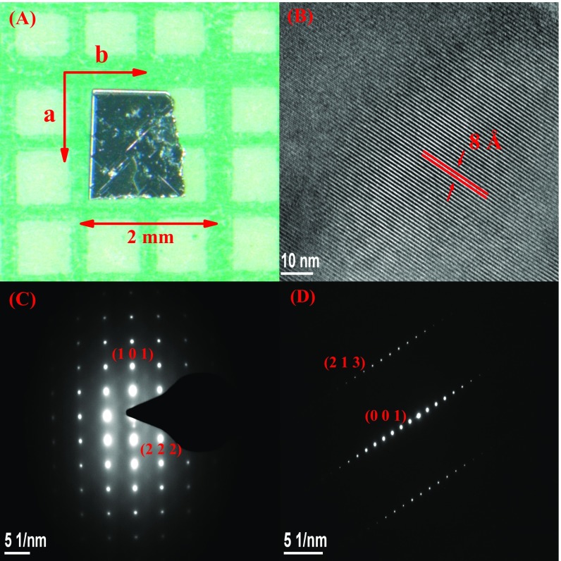
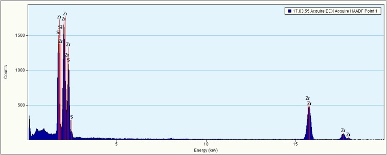
High-resolution transmission electron microscopy (HRTEM) and energy-dispersive X-ray (EDX) spectroscopy reveal high quality of the ZrSiS single crystals without any impurity. The details are given in SI Materials and Methods, SI Sample Characterization (Figs. S1 and S2).
Fig. S1.
(A) ZrSiS single crystal with different crystallographic directions. (B) HRTEM image along the ac plane. (C and D) Selected area electron diffraction (SAED) pattern obtained through HRTEM measurement.
Fig. S2.
Single-crystal EDX spectroscopy data.
Temperature Dependence of Resistivity.
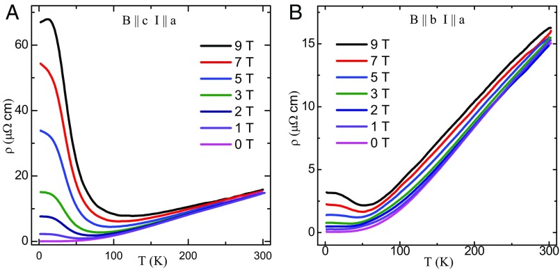
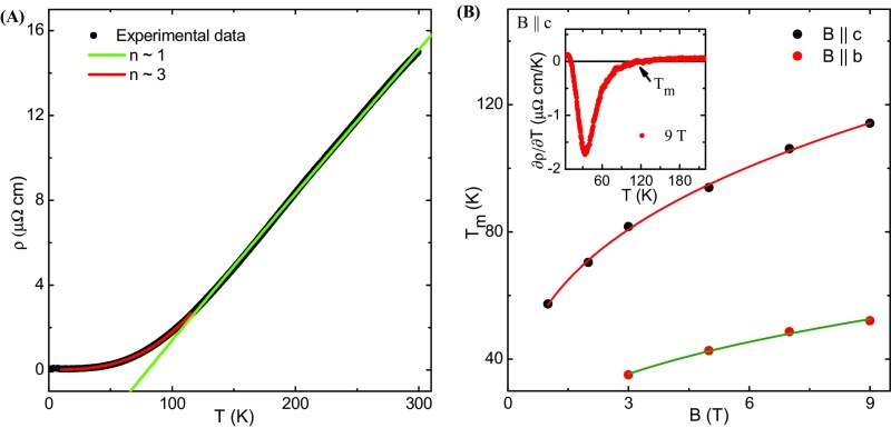
As shown in Fig. 1A, the zero-field resistivity of ZrSiS shows metallic character. decreases monotonically with the decrease in T down to 2 K. The resistivity at 2 K becomes as low as 52 n cm, which is comparable to that reported for Cd3As2 (10). At temperatures below 10 K, the measured resistivity shows some fluctuations within the instrument resolution, which can be explained in terms of the quantum ballistic transport (21). The ultralow residual resistivity and signature of quantum ballistic transport suggest that the mean free path of the charge carriers is very large. Hence, the impurity effect in ZrSiS is almost negligible. The residual resistivity ratio (300 K)/(2 K) is found to be 288, which is quite large and confirms good metallicity and high quality of the crystals. The resistivity data, in the temperature range 10–115 K, can be fitted well with the expression with n 3, as shown in Fig. S3A (SI Materials and Methods, Magnetotransport Properties). This indicates a deviation from a pure electronic correlation-dominated scattering mechanism (n = 2) (22). A similar type of temperature dependence of has also been observed in unconventional semimetals LaSb (n = 4) (23) and LaBi (n = 3) (24) and has been attributed to interband electron–phonon scattering. (T) is linear in the high-temperature region above 115 K. With the application of a magnetic field, the low-temperature resistivity undergoes a drastic enhancement, reflecting a metal–semiconductor-like crossover even at a field of 1 T only. This type of magnetic field-induced crossover is often described as a result of gap opening at the band-touching points in topological semimetals (14, 23–26). It is evident from Fig. 1B that the metal–semiconductor-like crossover is extremely sensitive to the direction of applied field. With current along the a axis and magnetic field parallel to the c axis, a strong crossover has been seen. On the other hand, rotating the field direction by 90°, i.e., parallel to the b axis, results in much weaker crossover, which occurs at higher field strength. In both the cases, the crossover temperature (Tm) increases monotonically with field and is showing -type relation (Fig. S3B) (SI Materials and Methods, Magnetotransport Properties). has a value 3 for both the applied field directions and deviates from the value = 2 for compensated semimetals Bi, WTe2, and graphite (27, 28). Considering the thermal activated transport as in the case of intrinsic semiconductor (29), , we have calculated the values of the thermal activation energy gap 20.2 meV and 3.7 meV at 9 T, for field directions along the c axis and the b axis, respectively (Fig. S4 A and B). The calculated gap Eg shows strong magnetic field dependence (Fig. S4C) (SI Materials and Methods, Magnetotransport Properties). For both the directions, below Tm, the resistivity exhibits an inflection followed by a plateau region. A similar low-temperature resistivity plateau has been observed in other topological semimetals and is independent of the sample quality (14, 23–26). Therefore, this low-temperature resistivity saturation is an intrinsic property of topological semimetals. However, the origin of this behavior is not yet settled (23).
Fig. 1.
Temperature dependence of resistivity measured under different transverse magnetic fields. (A) B c axis; (B) B b axis.
Fig. S3.
(A) Temperature dependence of zero-field resistivity. The experimental data are fitted using (B) Field dependence of metal–semiconductor crossover temperature for two field directions. B, Inset shows the temperature dependence of /T at a field of 9 T, applied parallel to the c axis. The point where the curve crosses the x axis indicates the crossover temperature (Tm).
Fig. S4.
ln() is plotted against T−1 at different transverse magnetic fields for (A) B c axis and (B) B b axis. (C) Magnetic field dependence of energy gap for two different field directions. Error bars represent the maximum change in Eg, when we change the linear fitting range. (D) Kohler’s rule scaling of MR data with field parallel to the c axis.
Extreme Transverse Magnetoresistance.
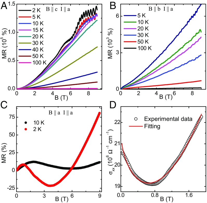
The transverse magnetoresistance (TMR), i.e., the change in resistance with magnetic field applied perpendicular to the current direction, has been measured at several temperatures. As illustrated in Fig. 2A, at some representative temperatures, with current parallel to the a axis and magnetic field along the c axis, an extremely large, nonsaturating magnetoresistance (MR) is obtained. At 2 K and 9 T, MR is 1.4 105%, which is comparable to that observed in several Dirac and Weyl semimetals (10, 13, 14, 25, 26). With the increase in temperature, MR decreases dramatically to a value of just about 14% at 300 K and 9 T. At low field, MR shows a quadratic field dependence ( B2), which becomes almost linear at higher field. As shown in Fig. S4D (SI Materials and Methods, Magnetotransport Properties), the MR data at different temperatures cannot be rescaled to a single curve, using Kohler’s rule MR = . The violation of Kohler’s rule suggests the presence of more than one type of carrier and/or the different temperature dependence of their mobilities (28, 30). Applying field parallel to the b axis and keeping the current direction unchanged, the MR at 9 T has been seen to reduce to 7,000% at 5 K (Fig. 2B). At 3 K and 9 T, the anisotropic ratio (B c)/(B b) has a large value of 21, which is comparable to that reported in NbSb2 (26). This result reflects strong anisotropy in electronic structure associated with the quasi-2D nature of the Fermi surface observed in ARPES (20). For a 2D system, where the charge is confined within the plane, the electronic motion is unaffected for the magnetic field parallel to the plane; i.e., the anisotropy in MR will be extremely large. On the other hand, the MR ratio is expected to be close to 1 for an isotropic 3D system.
Fig. 2.
(A and B) Transverse magnetoresistance with current along the a axis and magnetic field parallel to the (A) c axis and (B) b axis, measured at different temperatures, up to 9 T. (C) LMR with current and field along the a axis. (D) Fitting of longitudinal magnetoconductivity data at 2 K, using the semiclassical formula.
Longitudinal Magnetoresistance and Chiral Anomaly.
Next, the longitudinal MR (LMR) was measured with both the current and magnetic fields applied along the a axis. As shown in Fig. 2C, negative MR was observed at low field. With the increase in temperature, the negative MR progressively weakens. This negative MR has been ascribed to induced Adler–Bell–Jackiw chiral anomaly in Dirac systems, where a Dirac node splits into two Weyl nodes with opposite chirality due to broken TRS, under application of a magnetic field (8). Parallel magnetic (B) and electric (E) fields act as a nontrivial gauge field (E.B), which induces the chiral anomaly, i.e., charge imbalance between the two Weyl nodes of opposite chirality. This causes an extra flow of current along the direction of the applied electric field and results in the negative LMR. The chiral magnetic effect, a long-sought phenomenon proposed in relativistic quantum field theory, has been demonstrated in several 3D Dirac and Weyl semimetals such as Cd3As,SUB (31), Na3Bi (32), and TaAs (13). The field dependence of longitudinal conductivity [(Bx)] at a particular temperature can be analyzed using the semiclassical formula (13),
| [1] |
where and are the zero-field conductivity and resistivity at that temperature, respectively, and Cw is a temperature-dependent parameter originating from chiral anomaly. The term () takes care of the low-field minima in the conductivity, which is generally described as the effect of weak antilocalization in Dirac systems (13, 32), whereas the second term on the right-hand side includes the contribution from the nonlinear bands near the Fermi level. Fig. 2D illustrates the good agreement between the theoretical expression and experimental data. From Fig. 2C, it can be seen that the MR becomes positive at high field, which is due to small misalignment of E and B. The LMR at all temperatures can be well described using a misalignment angle 2°. The details are provided in SI Materials and Methods, Magnetotransport Properties (Fig. S5A). We also measured LMR with , along different crystallographic directions and on several crystals. For all of the cases, similar negative MR was observed, which confirms that negative LMR is associated with configuration rather than any particular crystallographic direction. In Fig. S5B, the measured LMR for the axis is shown as an example. Negative LMR has also been observed in a few systems other than Dirac or Weyl semimetals. However, in these systems the origin and nature of negative MR are completely different from chiral anomaly (SI Materials and Methods, Magnetotransport Properties).
Fig. S5.
(A) Fitting of high-field region of LMR (B I a), assuming a small misalignment angle between B and E. (B) LMR at 2 K with current and field along the b axis.
SdH Oscillation and Fermi Surface Properties.
Another interesting feature that emerges from the transport measurement is the presence of SdH oscillation traceable at fields even below 2 T and temperatures up to 20 K. This not only gives an insight into the nature of the Fermi surface, but also provides evidence of very high mobility of the associated charge carriers. From the TMR data, it is clear that there is more than one frequency. To extract the oscillatory component (B), a smooth background is subtracted from (B). To deconvolute the two components of oscillation, the background subtraction has been done in two steps.
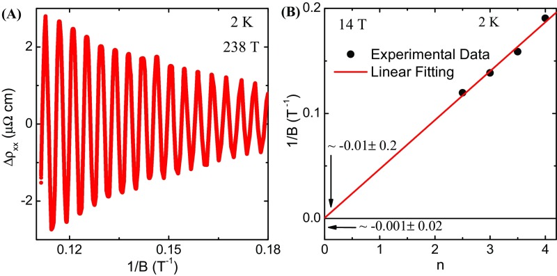
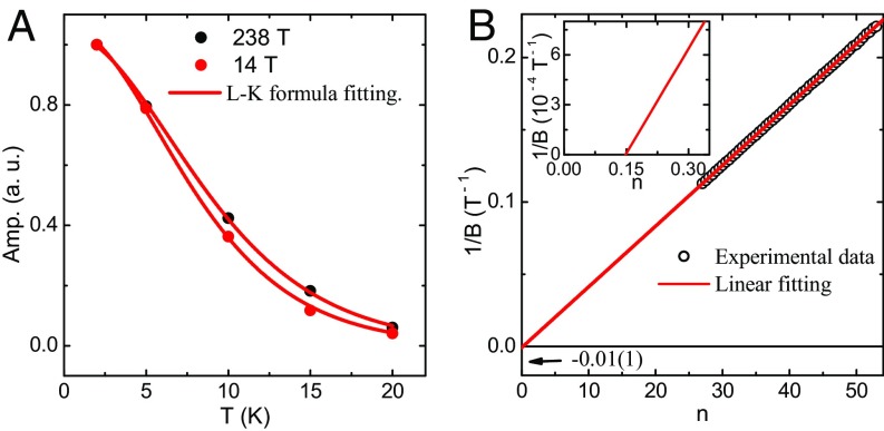
In Fig. 3 A and B, (B), for two different components, is plotted as a function of 1/B at several representative temperatures. As the oscillation peaks are very sharp and the field interval used in the measurements is not too small compared with the peak width, some fluctuations in the intensity have been observed in Fig. 3B. Using a much smaller field interval, we observed that the peak intensity becomes systematic (Fig. S6A). The fast Fourier transform (FFT) analysis of the oscillatory components reveals oscillation frequencies 14 T and 238 T. The obtained frequencies indicate the existence of a very large and a small Fermi surface cross-section perpendicular to the c axis. Using the Onsager relationship, , where is the magnetic flux quantum and is the Fermi surface cross-section perpendicular to the applied magnetic field, we have calculated cross-sections 1.4 ⋅ and for 14 T and 238 T frequencies, respectively. In Fig. 4A, the oscillation amplitude for both the frequencies is shown as a function of temperature and has been fitted using the thermal damping factor of the Lifshitz–Kosevich formula, , where = . From the fitting parameters, the cyclotron effective masses () of the charge carriers are determined to be 0.14 and 0.1 for 238 T and 14 T frequencies, respectively, where m0 is the rest mass of the free electron. To determine the approximate value of the carrier density, we used its relation with the oscillation frequency (33), , where and are the spin and valley degeneracies. We found the carrier densities () to be 2 1019 and 3 for the large and small Fermi pockets, respectively. From the magnetic field-induced damping of oscillation amplitude, , the Dingle temperatures () are determined to be 11.2 K and 3.4 K for the large and small Fermi pockets, respectively, at 2 K. To get a quantitative estimate about the mobility of the charge carriers in the system, we calculated the quantum mobility, . The obtained values cm2⋅⋅ and cm2⋅⋅ for the large and small frequencies, respectively, imply the significant difference between the mobilities of the carriers, which is expected due to different effective masses of the carriers associated with the Fermi pockets (mobility . The quantum mobility in a system is always lower than the classical Drude mobility (), as is sensitive to both large- and small-angle scattering, whereas is sensitive to only large-angle scattering (34). The extracted parameters from SdH oscillation are summarized in Table 1. With magnetic field along the b axis, no clear oscillation was recorded up to 9 T applied field. This may be due to heavier effective mass and low mobility of the charge carriers along that direction and/or the quasi-2D nature of the Fermi surface in ZrSiS.
Fig. 3.
(A and B) SdH oscillation obtained by subtracting the smooth background from the MR measurement, plotted with inverse magnetic field (1/B) at different temperatures for the two deconvoluted components. A and B, Insets show the corresponding FFT results. (C) The angle dependence of oscillation frequencies. For clarity, FFT results for different angles are shifted vertically. The schematic of the experimental setup is shown in C, Inset.
Fig. S6.
(A) The SdH oscillation at 2 K for 238-T frequency, measured with very small field interval. (B) Landau-level index plot for 14-T frequency. Arrows show the values of x- and y-axis intercepts.
Fig. 4.
(A) Temperature dependence of relative amplitude of SdH oscillation for both the Fermi pockets. (B) Landau-level index plot for 238-T frequency oscillation. B, Inset shows the x-axis intercept by extrapolated linear fitting. Arrow shows the value of the y-axis intercept.
Table 1.
Parameters extracted from SdH oscillation for two Fermi pockets (34)
| F | l | |||||
| T | 105 m/s | nm | 103 cm2/Vs | 1017 | ||
| 238 | 8.5 | 0.14 | 2.4 | 25.7 | 1.3 | 200 |
| 14 | 2 | 0.1 | 6.9 | 247.4 | 6.2 | 3 |
kF, vF, and l are the Fermi momentum, Fermi velocity, and mean free path of the charge carriers, respectively.
Angle Dependence of Oscillation Frequencies.
For deeper understanding of the Fermi surface geometry, we performed angle-resolved TMR measurements and SdH oscillation analysis. The resultant FFT spectra for different directions are shown in Fig. 3C. Fig. 3C, Inset illustrates the experimental setup with current along the a axis and magnetic field rotated in the bc plane. As illustrated in Fig. 3C, the low-frequency component Fα (14 T) remains invariant with increasing angle up to 20°, after which it bifurcates into two very closely spaced frequency components. However, with further increase in angle, they come close to each other and merge to become a single frequency. On the other hand, the high-frequency component Fβ (238 T) splits into two components (Fδ and Fε), which are well separated in the frequency spectra. Whereas the higher one (Fε) among the two disappears above a certain angle, Fδ is seen to shift toward a lower value and then bifurcates (Fω and Fϕ). As already discussed, with current along the a axis and magnetic field along the b axis (), no clear oscillatory component was found.
Berry Phase and Zeeman Splitting.
In an external magnetic field, a closed orbit is quantized following the Lifshitz–Onsager quantization rule (35), , where 2 is Berry’s phase and is a phase shift determined by the dimensionality, having values 0 and 1/8 for 2D and 3D cases, respectively. The nature of the electronic band dispersion is determined by the value of the Berry phase, which is 0 for the conventional metals with parabolic band dispersion and for the Dirac/Weyl-type electronic system with linear band dispersion. The quantity can be extracted from the x-axis (along which the Landau-level index n has been plotted) intercept in the Landau-level fan diagram and takes a value in the range −1/8 to +1/8 for 3D Dirac fermions (35). In Fig. 4B, the Landau-level fan diagram for the larger Fermi pocket in ZrSiS is plotted, assigning maxima of the SdH oscillation as integers (n) and minima as half-integers (n + 1/2). Extrapolated linear fitting gives an intercept of 0.15(3) (Fig. 4B, Inset). The sharp, symmetric, and well-separated oscillation peaks over a wide range (n = 27–53) and traceable down to 4 T imply no significant error in determining the value of the intercept from the linear n vs. 1/B fit. On the other hand, with a higher magnetic field to achieve lower Landau level, the nonlinearity in the index plot may arise due to the Zeeman splitting of oscillation peaks as observed for 14-T frequency and discussed below. Similar to that observed for 238-T frequency, a small intercept −0.01 is obtained for 14-T frequency and shown in Fig. S6B (SI Materials and Methods, Magnetotransport Properties). For both the Fermi pockets, the intercepts are very close to the range 1/8. For the smaller frequency, the experimental peak positions are seen to deviate slightly from a straight line that can be attributed to the Zeeman splitting of the Landau levels (34, 36). Although the presence of Zeeman splitting is not clearly visible in the SdH oscillation, the spin–split peaks can be easily distinguished in the de Haas–van Alphen (dHvA) oscillation in our magnetization measurements (Fig. S7 A and B) (SI Materials and Methods, Magnetotransport Properties). Taking the peak and valley positions of the lower-field oscillations, which are almost free from the Zeeman splitting, we also plotted the Landau-level fan diagram for smaller frequency from dHvA oscillation (Fig. S7C) and obtained a small intercept, 0.05(2). Furthermore, we calculated Berry’s phase from the SdH oscillations at different angles (up to 20°) and did not find any significant change. Finding a reasonably accurate value of Berry’s phase for higher angles is much more complicated due to the presence of multiple oscillation frequencies.
Fig. S7.
(A) The dHvA oscillation at 2 K, obtained after background subtraction. (B) Oscillatory part of the magnetic susceptibility for the smaller frequency. (C) The Landau index n + 1/4 plot against 1/B for the smaller frequency. Arrows show the values of x- and y-axis intercepts.
Hall Measurement.
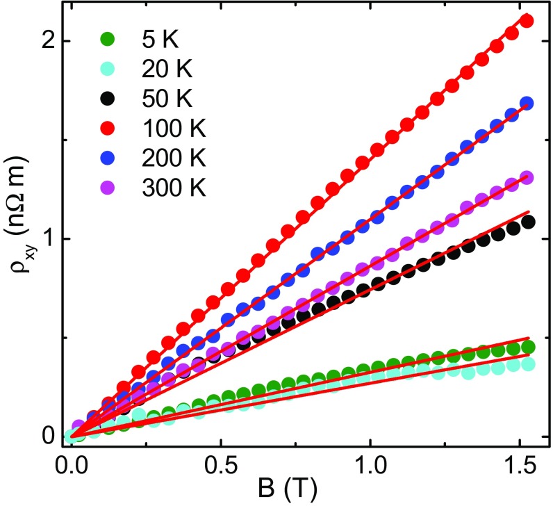
To determine the nature of the charge carriers of two Fermi pockets, the Hall effect measurement was performed. At 300 K, the Hall resistivity is found to be almost linear with field and positive (Fig. 5A), which indicate holes as majority carriers, consistent with the earlier ARPES report (20). With decreasing temperature, the Hall resistivity develops a sublinear character and at around 50 K it changes sign from positive to negative at high magnetic field, confirming the existence of more than one type of carrier. The overall behavior of the Hall resistivity can be explained by considering low-mobility holes and higher-mobility electrons associated with large and small Fermi pockets, respectively. Following the classical two-band model (37), the Hall resistivity is fitted in Fig. S8 (SI Materials and Methods, Two-Band Fitting of the Hall Resistivity). Obtained electron and hole densities, 1.6 1017 and 6 1019 , respectively, are in agreement with those calculated from SdH oscillation. As expected, at 5 K, large electron mobility ∼2 × 10⁴ ⋅⋅ and hole mobility 2.8 103 ⋅s−1 have been obtained from the fitted parameters. From the Hall resistivity, it is clear that at least two band crossings are present in the electronic band structure of ZrSiS at different energy values, as shown schematically in Fig. 5B. The earlier reports on ARPES and band structure calculations suggest the presence of multiple Dirac crossings at different energy values as illustrated in the schematic in Fig. 5C. As shown, the Dirac cones 1 and 2 cross the Fermi energy, having Dirac points at two different energy values. Among the rest, cones 3 and 4 have their band crossing points almost at the chemical potential with negligible Fermi surface, whereas cones 5 and 6 are lying well below the Fermi energy. Thus, in this configuration, it is expected that only Dirac cones 1 and 2 will contribute to the transport properties of ZrSiS, which is consistent with our magnetotransport results.
Fig. 5.
(A) Field dependence of the Hall resistivity measured at different temperatures. (B) Schematic explaining transport measurement results. (C) Schematic illustrating multiple Dirac cones in ZrSiS as described in earlier reports (19, 20).
Fig. S8.
Hall resistivity as a function of the magnetic field. The solid lines are a classical two-band model fit to the experimental data.
SI Materials and Methods
Single crystals of ZrSiS were grown in two steps via iodine vapor transport. At first, the polycrystalline powder was synthesized using elemental Zr (Alfa Aesar 99.9%), Si (Strem Chem. 99.999%), and S (Alfa Aesar 99.9995%). The details are described elsewhere (41). Then the polycrystalline powder together with iodine in a concentration of 5 mg/cm3 was sealed in a 20-cm-long quartz tube under vacuum. The quartz tube was kept in a gradient furnace for 72 h with the powder at 1,100 °C and the cooler end at 1,000 °C. Shiny rectangular plate-like crystals were obtained at the cooler end. HRTEM of the grown crystals was done in an FEI, TECNAI G2 F30, S-TWIN microscope operating at 300 kV and equipped with a GATAN Orius SC1000B CCD camera. EDX spectroscopy of the grown ZrSiS crystals was performed using the same microscope with a scanning unit and a high-angle annular dark-field scanning (HAADF) detector from Fischione (Model 3000). Transport measurements were performed via a four-probe technique in a 9-T Physical Property Measurement System (Quantum Design) in ac transport option as well as in a 9-T cryogen-free measurement system (Cryogenic) using a nanovoltmeter (Keithley). Magnetic measurements were done in a 7-T SQUID-VSM MPMS 3 (Quantum Design).
SI Sample Characterization.
In Fig. S1A, a single crystal of ZrSiS with typical dimensions 1.8 1 0.14 mm is shown with different crystallographic axes. The crystals cleave perpendicular to the c axis, similar to an earlier report (20). The HRTEM image of the crystal along the ac plane (Fig. S1B) confirms the high-quality crystalline nature and the layered structure of the lattice with interlayer distance. The electron diffraction patterns obtained in HRTEM are shown in Fig. S1 C and D with corresponding Miller indexes of the lattice planes. EDX spectroscopy (Fig. S2) verifies almost perfect stoichiometry and absence of any impurity in the grown crystals. Magnetotransport measurements were done on several crystals from the same batch, which reproduced similar results.
Magnetotransport Properties.
The zero-field resistivity shows two regions with different temperature dependence. As shown in the Fig. S3A, the resistivity obeys dependence at low temperature, which is followed by almost linear dependence at high temperature.
Field-induced metal–semiconductor crossover is indicated by the increase in resistivity with decreasing temperature in the presence of the magnetic field. The crossover temperature () is identified as the temperature where resistivity shows the minimum, i.e., the temperature where /T becomes zero. The magnetic field dependence of is shown in Fig. S3B. For both the applied field directions, is seen to be .
The logarithmic behavior of resistivity with inverse temperature is shown in Fig. S4 A and B for magnetic field applied along two different crystallographic directions. At the point of metal–semiconductor-like crossover, the sign of the slope changes. From the slope of the curves at the linear regions, the values of thermal activation energy () have been calculated. As the curves are linear over a very small temperature range, the calculated gap depends on the region of linear fitting and hence becomes a function of T. Following Tafti et al. (42), we have calculated the energy gap at different temperature regions. The error bar in Fig. S4C represents the maximum change in , when we change the linear fitting range. The calculated energy gap exhibits magnetic field dependence for both the directions of the applied field.
As shown in Fig. S4D, the MR data were plotted as a function of . The curves at different temperatures do not merge, indicating the violation of Kohler’s rule in ZrSiS.
Fig. S5A illustrates the LMR of ZrSiS. MR becomes positive at higher fields, which is due to the small misalignment of E and B. Therefore, a competition between the negative LMR and positive TMR components occurs. As both of these components have different temperature dependence and TMR decreases more rapidly with increasing temperature, the minimum in MR shifts toward a higher field with increasing temperature. By fitting the high-field region of MR, a small misalignment angle ∼2° is determined for all of the temperatures. Similar behavior was observed when E and B both are applied along arbitrary crystallographic directions in the ab plane. As an example, in Fig. S5B the LMR at 2 K is shown with E and B along the b axis. Besides the Dirac and Weyl semimetals, a few ultraclean layered materials such as PdCoO2, PtCoO2, and Sr2RuO4 also show negative LMR (43). However, the nature of the observed negative MR in these compounds is completely different from that originated from chiral anomaly. In these layered materials, negative MR appears when E and B are along a certain crystallographic direction. For other directions, MR is positive, even for parallel E and B configuration, unlike Dirac and Weyl semimetals. For example, in PdCoO2 and PtCoO2, the negative MR is observed only when EBc axis or B is close to a Yamaji angle and in Sr2RuO4 only when E and B are within 10° of the c axis. Moreover, in these systems, the MR decreases linearly with increasing field from its zero-field value. On the other hand, the chiral anomaly-induced negative MR in 3D Dirac and Weyl semimetals is quadratic in field as described by Eq. 1 in the main text.
As shown in Fig. 3B, some fluctuations in the amplitude of the SdH oscillation peaks have been observed for the 238-T frequency component. These fluctuations are prominent at 2 K but not so clearly visible for other temperatures. As the oscillation peaks are very sharp and the field interval used in the measurements is not too small compared with the peak width, it is expected that some fluctuations would appear in the peak intensity. The peak intensity becomes systematic when we measured with a much smaller field interval (Fig. S6A). However, we did not observe any visible change in peak positions. Moreover, the positions of the fluctuations are completely random and change when the field interval is changed.
The Landau-level index plot for the smaller Fermi pocket is shown in Fig. S6B. Due to the weak nonlinearity in the index plot, the intercept was obtained from the best linear fit. Although this method introduces some error in the observed intercept, even with maximum error (0.18), which was calculated from the linear fitting of the first three and last three points, the intercept is close to the previously mentioned theoretical range and far from that expected for the conventional quadratic band (0.5). The small deviation in the experimental data from the straight line is a consequence of the unequally spaced maxima/minima in SdH oscillation (Fig. 3A) and likely occurs due to the Zeeman splitting. The spin–split peaks can be clearly seen in the dHvA oscillation (Fig. S7A). In Fig. S7B, the oscillatory part of magnetic susceptibility = dM/dB is plotted for the smaller frequency, after subtracting the background. For the Landau-level fan diagram, if we assume integer indexes n for maxima in M, the maxima in correspond to n + 1/4 (44). Therefore, the Landau level index n + 1/4 is plotted in Fig. S7C for smaller frequency, taking the peak and valley positions of the lower-field oscillations, which are almost free from the Zeeman splitting. The linear nature of the index plot indicates almost no error in the obtained intercept. From Fig. S7C, a small intercept of 0.05(2) is obtained, which confirms the Dirac fermionic nature of the charge carriers associated to the small Fermi pocket.
Two-Band Fitting of the Hall Resistivity.
To calculate the classical Drude mobility of the charge carriers, the experimental Hall data are fitted (Fig. S8) using the two-band model,
| [1] |
in the low-field limit (45). () and () are the hole (electron) mobilities and densities, respectively. The calculated parameters are in agreement with those obtained from the quantum oscillation and listed in Table 1 of the main text.
Why It Is Important to Study the Other Members of the WHM Family.
ZrSiS represents a large family of materials (WHM with W = Zr, Hf; H = Si, Ge, Sn; M = O, S, Se, Te) with identical crystal structure (PbFCl type). Recently, this family has been theoretically proposed as a potential candidate for a 2D topological insulator (19). However, subsequent ARPES measurement has revealed multiple bulk band crossings with linear dispersion over a wide energy range and a 3D Dirac line node in ZrSiS (20). Topological nodal line fermions have been observed in very few systems, where the strength of spin–orbit coupling (SOC) plays a crucial role in protecting the line nodes (18). Therefore, with increasing atomic number, for example from Zr (Z = 40) to Hf (Z = 72), it is expected that the increasing SOC will substantially affect the topological protection of the nontrivial electronic band structure. Furthermore, as M changes from O to Te, it has been seen that the particle–hole asymmetry increases and the interlayer binding energy decreases (19). Whereas lower particle–hole asymmetry introduces a global band gap, weaker interlayer coupling enhances the monolayer characteristic in electronic properties of the system. So it may experimentally be possible to realize a 2D topological insulating phase in other members of the family and will require further investigations. In this context, the present work explicitly describes the different unusual electronic properties in ZrSiS and may pave the way to subsequent rigorous study on other members of this group.
Summary
In conclusion, we present the systematic study of the magneto-electronic transport properties on ZrSiS single crystals. Magnetic field-induced metal–semiconductor-like crossover along with strongly anisotropic transport properties have been observed. The anisotropic MR along different crystallographic axes is in good agreement with the quasi-2D nature of the Fermi surface observed in ARPES. TMR approaches an extremely large value 1.4 105% at 2 K and 9 T, without any sign of saturation. Under parallel E and B configuration, the observed negative MR implies Adler–Bell–Jackiw chiral anomaly of 3D Dirac fermions in ZrSiS. The SdH oscillation reveals two inequivalent Fermi surface cross-sections perpendicular to the crystallographic c axis. The Dirac fermionic nature of the charge carriers is also confirmed from the observed nontrivial Berry phase in the Landau-level fan diagram for both the Fermi pockets. Nonlinear field dependence of Hall resistivity indicates the presence of both electron- and hole-type charge carriers. Classical two-band fitting of Hall resistivity reveals high mobilities for both types of charge carrier. SdH oscillation along with Hall measurement reflects multiple band crossings at different energy values of the electronic band structure. We believe the present work not only makes a substantive experimental contribution in this contemporary area of research but also can encourage further extensive works in ZrSiS and other members of the family.
During the submission process of our manuscript, several reports on magnetotransport and magnetization measurements in ZrSiS were submitted to arXiv.org (38–40), supporting the major conclusions of our work.
Materials and Methods
The single crystals were grown by a standard iodine vapor transport technique and characterized using HRTEM and EDX spectroscopy. The transport measurements were performed in PPMS (Quantum Design) and a cryogen-free system (Cryogenic) via a four-probe technique. Magnetic measurements were done in MPMS3 (Quantum Design). See SI Materials and Methods for details.
Acknowledgments
We thank N. Khan, A. Paul, and S. Roy for their help during measurements and useful discussions.
Footnotes
The authors declare no conflict of interest.
This article is a PNAS Direct Submission.
This article contains supporting information online at www.pnas.org/lookup/suppl/doi:10.1073/pnas.1618004114/-/DCSupplemental.
References
- 1.Hasan MZ, Kane CL. Colloquium: Topological insulators. Rev Mod Phys. 2010;82(4):3045–3067. [Google Scholar]
- 2.Liu ZK, et al. A stable three-dimensional topological Dirac semimetal Cd3As2. Nat Mater. 2014;13(7):677–681. doi: 10.1038/nmat3990. [DOI] [PubMed] [Google Scholar]
- 3.Xu SY, et al. Discovery of a Weyl fermion semimetal and topological Fermi arcs. Science. 2015;349(6248):613–617. doi: 10.1126/science.aaa9297. [DOI] [PubMed] [Google Scholar]
- 4.Daughton JM. GMR applications. J Magn Magn Mater. 1999;192(2):334–342. [Google Scholar]
- 5.Wolf SA, et al. Spintronics: A spin-based electronics vision for the future. Science. 2001;294(5546):1488–1495. doi: 10.1126/science.1065389. [DOI] [PubMed] [Google Scholar]
- 6.Lenz J. A review of magnetic sensors. Proc IEEE. 1990;78(6):973–989. [Google Scholar]
- 7.Wang Z, et al. Dirac semimetal and topological phase transitions in A3Bi (A=Na, K, Rb) Phys Rev B. 2012;85(19):195320. [Google Scholar]
- 8.Wang Z, Weng H, Wu Q, Dai X, Fang Z. Three-dimensional Dirac semimetal and quantum transport in Cd3As2. Phys Rev B. 2013;88(12):125427. [Google Scholar]
- 9.Neupane M, et al. Observation of a three-dimensional topological Dirac semimetal phase in high-mobility Cd3As. Nat Commun. 2014;5:3786. doi: 10.1038/ncomms4786. [DOI] [PubMed] [Google Scholar]
- 10.Liang T, et al. Ultrahigh mobility and giant magnetoresistance in the Dirac semimetal Cd3As. Nat Mater. 2015;14(3):280–284. doi: 10.1038/nmat4143. [DOI] [PubMed] [Google Scholar]
- 11.Liu ZK, et al. Discovery of a three-dimensional topological Dirac semimetal, Na3Bi. Science. 2015;343(6173):864–867. doi: 10.1126/science.1245085. [DOI] [PubMed] [Google Scholar]
- 12.Weng H, Fang C, Fang Z, Bernevig BA, Dai X. Weyl semimetal phase in noncentrosymmetric transition-metal monophosphides. Phys Rev X. 2015;5(1):011029. [Google Scholar]
- 13.Huang X, et al. Observation of the chiral-anomaly-induced negative magnetoresistance in 3d Weyl semimetal TaAs. Phys Rev X. 2015;5(3):031023. [Google Scholar]
- 14.Shekhar C, et al. Extremely large magnetoresistance and ultrahigh mobility in the topological Weyl semimetal candidate NbP. Nat Phys. 2015;11(8):645–649. [Google Scholar]
- 15.Borisenko S, et al. 2015. Time-reversal symmetry breaking type-II Weyl state in YbMnBi2. arXiv:1507.04847.
- 16.Kim Y, Wieder BJ, Kane CL, Rappe AM. Dirac line nodes in inversion-symmetric crystals. Phys Rev Lett. 2015;115(3):036806. doi: 10.1103/PhysRevLett.115.036806. [DOI] [PubMed] [Google Scholar]
- 17.Bian G, et al. Drumhead surface states and topological nodal-line fermions in TlTaSe2. Phys Rev B. 2016;93(12):121113(R). [Google Scholar]
- 18.Bian G, et al. Topological nodal-line fermions in spin-orbit metal PbTaSe2. Nat Commun. 2016;7:10556. doi: 10.1038/ncomms10556. [DOI] [PMC free article] [PubMed] [Google Scholar]
- 19.Xu Q, et al. Two-dimensional oxide topological insulator with iron-pnictide superconductor LiFeAs structure. Phys Rev B. 2015;92(20):205310. [Google Scholar]
- 20.Schoop LM, et al. Dirac cone protected by non-symmorphic symmetry and three-dimensional Dirac line node in ZrSiS. Nat Commun. 2016;7:11696. doi: 10.1038/ncomms11696. [DOI] [PMC free article] [PubMed] [Google Scholar]
- 21.Zhao Y, et al. Anisotropic Fermi surface and quantum limit transport in high mobility three-dimensional Dirac semimetal Cd3As2. Phys Rev X. 2015;5(3):031037. [Google Scholar]
- 22.Ziman JM. 2001. Electrons and Phonons, Classics Series (Oxford Univ Press, New York)
- 23.Tafti FF, Gibson QD, Kushwaha SK, Haldolaarachchige N, Cava RJ. Resistivity plateau and extreme magnetoresistance in LaSb. Nat Phys. 2016;12(3):272–277. [Google Scholar]
- 24.Sun S, Wang Q, Guo PJ, Liu K, Lei H. 2016. Large magnetoresistance in LaBi: Origin of field-induced resistivity upturn and plateau in compensated semimetals. arXiv:1601.04618v1.
- 25.Ali MN, et al. Large, non-saturating magnetoresistance in WTe2. Nature. 2014;514(7521):205–208. doi: 10.1038/nature13763. [DOI] [PubMed] [Google Scholar]
- 26.Wang K, Graf D, Li L, Wang L, Petrovic C. Anisotropic giant magnetoresistance in NbSb2. Sci Rep. 2014;4:7328. doi: 10.1038/srep07328. [DOI] [PMC free article] [PubMed] [Google Scholar]
- 27.Kopelevich Y, Pantoja JCM, da Silva RR, Moehlecke S. Universal magnetic-field-driven metal-insulator-metal transformations in graphite and bismuth. Phys Rev B. 2006;73(16):165128. [Google Scholar]
- 28.Wang YL, et al. Origin of the turn-on temperature behavior in WTe2. Phys Rev B. 2015;92(18):180402(R). [Google Scholar]
- 29.Hu J, Rosenbaum TF. Classical and quantum routes to linear magnetoresistance. Nat Mater. 2008;7(9):697–700. doi: 10.1038/nmat2259. [DOI] [PubMed] [Google Scholar]
- 30.McKenzie RH, Qualls JS, Han SY, Brooks JS. Violation of Kohler’s rule by the magnetoresistance of a quasi-two-dimensional organic metal. Phys Rev B. 1998;57(19):11854. [Google Scholar]
- 31.Li H, et al. Negative magnetoresistance in Dirac semimetal Cd3As2. Nat Commun. 2016;7:10301. doi: 10.1038/ncomms10301. [DOI] [PMC free article] [PubMed] [Google Scholar]
- 32.Xiong J, et al. Evidence for the chiral anomaly in the Dirac semimetal Na3Bi. Science. 2015;350(6259):413–416. doi: 10.1126/science.aac6089. [DOI] [PubMed] [Google Scholar]
- 33.Shoenberg D. Magnetic Oscillations in Metals. Cambridge Univ Press; Cambridge, UK: 1984. [Google Scholar]
- 34.Narayanan A, et al. Linear magnetoresistance caused by mobility fluctuations in n-doped Cd3As2. Phys Rev Lett. 2015;114(11):117201. doi: 10.1103/PhysRevLett.114.117201. [DOI] [PubMed] [Google Scholar]
- 35.Murakawa H, et al. Detection of Berry’s phase in a bulk rashba semiconductor. Science. 2013;342(6165):1490–1493. doi: 10.1126/science.1242247. [DOI] [PubMed] [Google Scholar]
- 36.Taskin AA, Ando Y. Berry phase of nonideal Dirac fermions in topological insulators. Phys Rev B. 2011;84(3):035301. [Google Scholar]
- 37.Hurd CM. The Hall Effect in Metals and Alloys. Plenum; New York: 1972. [Google Scholar]
- 38.Ali MN, et al. 2016. Butterfly magnetoresistance, quasi-2D Dirac Fermi surfaces, and a topological phase transition in ZrSiS. arXiv:1603.09318v2.
- 39.Wang X, et al. 2016. Evidence of both surface and bulk Dirac bands in ZrSiS and the unconventional magnetoresistance. arXiv:1604.00108.
- 40.Hu J, et al. 2016. Evidence of Dirac cones with 3D character probed by dHvA oscillations in nodal-line semimetal ZrSiS. arXiv:1604.01567.
- 41.Haneveld AK, Jellinek F. Zirconium silicide and germanide chalcogenides preparation and crystal structures. Recl Trav Chim Pays Bas. 1964;83(8):776–783. [Google Scholar]
- 42.Tafti FF, et al. Temperature-field phase diagram of extreme magnetoresistance. Proc Natl Acad Sci USA. 2016;113(25):E3475–E3481. doi: 10.1073/pnas.1607319113. [DOI] [PMC free article] [PubMed] [Google Scholar]
- 43.Kikugawa N, et al. Interplanar coupling-dependent magnetoresistivity in high-purity layered metals. Nat Commun. 2016;7:10903. doi: 10.1038/ncomms10903. [DOI] [PMC free article] [PubMed] [Google Scholar]
- 44.Ando Y. Topological insulator materials. J Phys Soc Jpn. 2013;82(10):102001. [Google Scholar]
- 45.Huynh KK, Tanabe Y, Tanigaki K. Both electron and hole Dirac cone states in Ba(FeAs)2 confirmed by magnetoresistance. Phys Rev Lett. 2011;106(21):217004. doi: 10.1103/PhysRevLett.106.217004. [DOI] [PubMed] [Google Scholar]


