Abstract
We report on a thickness-dependent wetting property of WS2/Al2O3 and WS2/SiO2/Si structures. We prepared WS2 films with gradient thickness by annealing thickness-controlled WO3 films at 800 °C in sulfur atmosphere. Raman spectroscopy measurements showed step-like variation in the thickness of WS2 over substrates several centimeters in dimension. On fresh surfaces, we observed a significant change in the water contact angle depending on film thickness and substrate. Transmission electron microscopy analysis showed that differences in the surface roughness of WS2 films can account for the contrasting wetting properties between WS2/Al2O3 and WS2/SiO2/Si. The thickness dependence of water contact angle persisted for longer than 2 weeks, which demonstrates the stability of these wetting properties when exposed to air contamination.
Keywords: WS2, Wetting property, Morphology control, Chemical vapor deposition, Raman spectroscopy, Transmission electron microscopy
Background
Layered transition metal dichalcogenides (TMDs), such as MX 2 (M = Mo or W, X = S, Se, or Te), have intriguing transition behaviors in electronic structures and optical properties, subject to layer thickness. TMDs have been intensively explored for diverse applications, such as transparent flexible devices [1–8], valleytronics [9, 10], and optoelectronics [11–15]. Other important aspects of TMDs are their tribological properties, such as friction and wetting characteristics. By understanding the tribological aspects, one may control liquid-solid interface in nanoscale sensors [16] and make self-cleaning surfaces on transparent electronic devices [17, 18]. Such applications, especially, demand air exposure stability of the film surfaces, because the surfaces should be exposed to liquid-solid interaction either for attracting or repelling liquid droplets. Among the layered materials, WS2 powder lubricant is known to be useful in harsh conditions due to its high chemical stability compared to graphite and MoS2 powders [19–21].
Depending on the layer thickness, both graphene and TMDs show interesting wetting characteristics. To date, wetting has been understood in terms of several important parameters: wettability of supporting substrate, crystallinity or morphology of a TMD film, and airborne contaminants. Recently, Chow et al. suggested a model to understand the influence of these parameters as a function of two major types of interactions: short-range van der Waals interactions and long-range dipole-dipole interactions [22]. Based on this model, one could understand that flat, uniform TMD layers on SiO2/Si substrates show a strong thickness dependence of the water contact angle (CA). This thickness dependence becomes weakened after aging in air, and such aging effect is saturated after 7 days [22]. However, more drastic changes in wetting behavior could possibly be achieved by combining both wetting translucency and artificial nanoscale patterning. Such nanoscale patterning of the TMD layer could be realized by using photolithography and alternatively also by controlling the initial growth mode to obtain nanoscale islands [23].
Chemical vapor deposition (CVD) is a robust method for fabricating large-area TMD thin films and has the advantages of being low cost, scalable, and industry compatible [4, 24–26]. TMD thin films can be synthesized either by evaporating metal-oxide powder or by converting pre-deposited metal or metal-oxide films in the presence of chalcogen atmosphere. In particular, displacing the oxygen in pre-deposited metal-oxide films in chalcogen atmosphere has the advantage of obtaining continuous films with controlled film thickness. Moreover, controlling growth parameters, such as temperature, thickness, and substrate, can lead to a variety of film morphologies and crystallinity [4, 24, 27].
In this paper, we report on the synthesis of WS2 films where different surface morphologies were obtained by employing different substrates (SiO2/Si and Al2O3). By adopting a step-like wedge growth method, we tested the influence of film thickness and underlying substrate on the behavior of the water CA. We find that the crystallinity of the substrate determines surface roughness and the continuity of the as-grown films, which strongly affects the interaction of water with the ultrathin films and underlying substrates. We also discuss the influence of airborne contaminants for the stability of the water CA.
Methods
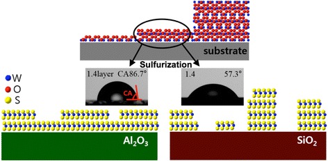
The WO3 thin films were deposited in an e-beam evaporator system (Korea Vacuum Tech) and sulfurized using CVD (Scientech). For evaporation of WO3, chunk pieces of WO3 (99.9%) were used as a source. The sapphire (Al2O3) (001) and SiO2/Si substrates with 300-nm-thick dry-oxidized SiO2 were thoroughly cleaned with acetone, ethanol, and deionized water. Before introducing the substrates into the e-beam evaporator chamber, the substrates were pre-annealed at 400 °C for 1 h in high vacuum (<5 × 10⁻⁷ Torr) to minimize surface adsorbents. The gradient-thickness WO3 films were deposited by using a manual shutter in front of the long pieces of substrate. A schematic diagram is shown in Fig. 1. WO3 films with step-like thickness variation were prepared with d WO3 = 0.5–10 nm. These films were then sulfurized in a CVD chamber at 800 °C for 1 h. During the whole CVD process, the total pressure was maintained at 0.5 Torr by mixing Ar and H2 gases with flow rates of 80 and 10 sccm, respectively. Similar sulfurization methods have been reported for fabrication of centimeter-scale WS2 films on SiO2/Si wafers and WSe2 films on Al2O3 wafers [24, 28–30].
Fig. 1.

Schematic diagram of a step-like thickness gradient WO3 film and the sulfurized WS2 films on Al2O3 and SiO2/Si substrates. Water contact angle (CA) images show different CAs on different substrates for 1.4 monolayer of WS2
The static water CA measurements were carried out on as-grown films by using a goniometer (Rame-hart, Model 200) with deionized water (>3 MΩ) at a temperature of 23 °C and 60% humidity. The CA measurements were repeated under similar conditions 20 days later to check the effect of aging due to air exposure.
The crystallinity and thickness were measured using a room temperature micro-Raman spectrometer (inVia, Renishaw). For the Raman measurement, the 514.5 nm excitation laser was first calibrated with the Si peak at 520.0 cm−1 as a reference and intensities were normalized to the main peak of WS2 at 355 cm−1. The film microstructure was studied using a transmission electron microscopy (TEM) (JEM-ARM200F, JEOL) with a Schottky-type field emission gun (FEG) operated at 200 keV. The cross-sectional specimens are prepared with conventional processes: cutting, gluing, polishing, and ion milling (PIPS 691, GATAN) operated at 5 keV.
Results and Discussion
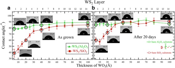
We found an interesting thickness dependence of the water CA values for WS2 films with SiO2/Si and Al2O3 substrates. To minimize the influence of airborne contaminants [31, 32], we measured the water CA on CVD as-grown samples within 2 h, by keeping the samples in a portable vacuum desiccator. Figure 2a shows the CA data obtained for the as-grown WS2/SiO2/Si and WS2/Al2O3 sample series. Both sample series showed gradual decrease of CA from d WO3 = 8 to 3 nm. Interestingly, below d WO3 = 3 nm, the CA of the WS2/SiO2/Si samples sharply decreased, while the CA of the WS2/Al2O3 samples decreased gradually. We note that the gradual decrease in CA was similar to observations in uniform WS2 films on SiO2/Si substrates, as reported earlier [22]. Such similarity suggested that the thickness dependence of CA may be more sensitive to the film morphology than to the underlying substrate.
Fig. 2.

Water CA measurements of a the as-grown WS2 films on Al2O3 and SiO2/Si substrates and of b the same samples after 20 days. Dashed lines indicate the CA values of bare Al2O3 (green) and SiO2/Si (red) substrates
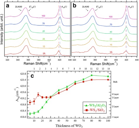
After the CA measurements on the as-grown samples, we carried out Raman spectroscopy measurements to analyze crystallinity and film thickness, as shown in Fig. 3. As d WO3 increases, the Raman spectrum shows a gradual change, indicating that the WS2 film thickness also varies with d WO3. We clearly observe blue shifting of the A1g peak (~420 cm−1) for both WS2/SiO2/Si and WS2/Al2O3 sample series. Figure 3c shows d WO3 dependence of the A1g peak positions, which is often used for estimating the WS2 layer thickness [24, 29, 33]. Both series showed a gradual decrease of the A1g peak as d WO3 decreased. However, there was a significant deviation between the two sample series for d WO3 < 3 nm. The strongest peak (near 355 cm−1) showed a gradual change in shape, corresponding to change in the ratio of intensities of two superposed peaks, 2LA (~352 cm−1) and E1 2g (~356 cm−1).
Fig. 3.

a Raman spectra from 0.5-nm- to 10-nm-thick WS2 grown on Al2O3 and b SiO2 substrate as a function of WO3 thickness (d WO3) (514.5 nm laser excitation, 300 K). The peaks at ~355 and ~420 cm−1 correspond to overlap of 2LA(M) and E1 2g(Γ) peaks and A1g(Γ) peak, respectively. Blue and red dashed lines indicate the A1g(Γ) peak position of the thick sample (d WO3 = 10 nm) and thin sample (d WO3 = 0.5 nm), respectively. Intensities are normalized with the A1g peaks. c Thickness dependence of the A1g(Γ) peak position
From the Raman spectrum analysis, we identified each sample with nominal WS2 film thickness, assuming a uniform film. As indicated in the right axis of Fig. 3c, we estimated WS2 layer thickness based on both the systematic shift of the A1g peak and the change in intensity ratio of 2LA and E1 2g peaks, compared with both the reported exfoliated and CVD-grown samples [24, 29, 33]. The WS2/Al2O3 sample series showed linear thickness variation between 2.1 and 5.7 monolayers (ML). However, the WS2/SiO2/Si sample series had significantly non-linear thickness variation for thickness ranging between 1.4 and 4.3 ML, which coincided with the range where there was significant deviation of thickness-dependent CA for very thin films, i.e., d WO3 < 3 nm.
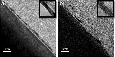
To check the film thickness and crystallinity, we performed cross section TEM analysis for both thin (d WO3 = 1.0 nm) and thick (d WO3 = 8.0 nm) samples for both substrates. Figure 4 shows the TEM images of the thin samples grown on (a) Al2O3 and (b) SiO2/Si substrates. The Al2O3 substrate supported a nearly continuous film with thickness between 1–3 ML, well in agreement with the nominal layer thickness of 1–2 ML, as shown in Fig. 3c. This uniform growth mode corresponds to a nearly linear shift of the A1g peak as a function of d WO3. On the other hand, the film on SiO2/Si substrate had several patches with thicknesses of 1–4 ML and lateral width of ~10 nm. Such nanoscale patches with thickness of a few MLs were consistent with the estimated thickness of 3 ML based on the Raman spectra for d WO3 < 3 nm, as shown in Fig. 3c. Therefore, we understand that very thin WS2 films grow with quite different growth modes during sulfurization, as schematically illustrated in the bottom of Fig. 1.
Fig. 4.

High-resolution transmission electron microscopy cross section images of WS2 (d WO3 = 1 nm) grown on a Al2O3 and b SiO2 substrates. Insets show corresponding image for the thick WS2 (d WO3 = 8 nm)
While very thin films showed contrasting film morphologies between two different substrates, thick films (d WO3 = 8.0 nm) on both substrates showed continuous film morphologies, as shown in insets of Fig. 4. This is also consistent with the Raman spectroscopy analysis, in which the films on both substrates showed nearly the same A1g peak values for thick films (see Fig. 3). By comparing the Raman spectroscopy and TEM results, we confirmed the nominal layer thicknesses of WS2 films, as indicated on the right axis in Fig. 3c. The relationship of WS2 layer thickness to d WO3 is indicated at the upper axis in Fig. 2.
Based on the differences in film morphology, we try to understand the interesting CA behavior. Previous reports about CA behavior on TMDs and graphene layers showed distinct thickness dependence between oxide and metal substrates due to differences in the charge screening of substrates. Here, we consider two models for oxide substrates: the uniform film model [22] and the growth-mode change model [31]. The uniform film model explains the gradual thickness dependence of CA for uniform TMD layers grown on SiO2/Si substrates. This model is consistent with our uniform WS2 layers on Al2O3 substrates. On the other hand, the growth-mode change model explains the larger thickness dependence of CA for rough TMD films, due to different crystal orientation and defects. This model well explains the sharper thickness dependence of CA for our rough WS2 films on SiO2/Si substrates. Therefore, we can reason that the growth-mode difference primarily affects the contrast of the change in CA for WS2 films on different substrates.
We note that the wetting transparency model also explains the strong thickness dependence of CA. C.-J. Shih et al. reported that 30% of the van der Waals interactions can be transmitted through the uniform ML graphene between water and the substrate [23]. In our uniform films on Al2O3 substrates, however, we observed only ~10% decrease in CA in the thinnest film compared to the thick film (~14 ML). This minute decrease of CA may be due to either the wetting transparency of uniform ML WS2 films or the aging process with absorption of airborne hydrocarbons [22]. However, the wetting transparency model cannot explain the strong thickness dependence of CA in the case of non-uniform films.
Furthermore, to understand the influence of airborne contaminants [32, 34], we repeated the CA measurements after keeping the samples in ambient conditions for 20 days, to exceed the air exposure saturation period of 1 week in the previous study [22]. As shown in the right-hand graphs of Fig. 2, extended air exposure diminished the overall thickness dependence of the water CA. For the WS2/Al2O3 samples with continuous morphology, the change in CA as a function of film thickness was smaller than the noise level. For the WS2/SiO2/Si samples with rough morphology, however, the distinct thickness dependence in CA persisted. The air exposure effect of continuous film is comparable with previous reports on the air susceptibility of continuous films with variable thickness, in which the air exposure influence is saturated after 1 week. The monolayer WS2, in particular, showed drastic aging behavior of CA within a few days, which made the thickness dependence of CA weak [22]. We note that further control experiment of air exposure by completion of sample preparation in the globe box is highly demanded as a future study.
However, we speculate that nanoscale crystallinity plays an important role for the air-stable CA behavior of the roughly grown films. The modified crystallinity at the nanoscale changes surface energy, which induces rather air-stable CA properties even on ultrathin film surface [29]. This robust thickness dependence of CA implies that one can selectively grow such rough morphology film to repel or attract liquid droplets, which becomes a building block of fluid control at nanoscale. Such air-stable thickness-dependent CA behavior could become important for applications, such as transparent electronic devices and microfluidic applications, where the surface tribological properties should be robust for extended exposure to atmosphere or liquid [17, 18, 31].
Conclusions
We fabricated ultrathin WS2 films with very different surface morphologies on different substrates, i.e., hexagonal crystalline Al2O3 (001) and amorphous SiO2. WS2 films with different surface morphologies showed distinct differences in the thickness dependence of the water CA. The thickness-dependent CA behaviors were stable following 20 days of air exposure. These transparent WS2 films should be useful for applications with transparent electronic devices.
Acknowledgements
This work is supported by the National Research Foundation of Korea (NRF) grants funded by the Korea Government (MSIP) (2014R1A1A1002868). This research was supported by Nanomaterial Technology Development Program through the National Research Foundation of Korea (NRF) funded by the Ministry of Science, ICT and Future Planning (2009-0082580).
Authors’ Contributions
YJC designed the experiments. BKC performed the sample preparations. BKC, IHL, and JK performed the sample characterizations. BKC and YJC analyzed the results and wrote the manuscript. All authors read and approved the final manuscript.
Competing Interests
The authors declare that they have no competing interests.
Consent for Publication
Not applicable.
Ethics Approval and Consent to Participate
Not applicable.
Publisher’s Note
Springer Nature remains neutral with regard to jurisdictional claims in published maps and institutional affiliations.
Abbreviations
- CA
Contact angle
- CVD
Chemical vapor deposition
- FEG
Field emission gun
- TEM
Transmission electron microscopy
- TMD
Transition metal dichalcogenide
Contributor Information
Byoung Ki Choi, Email: bk901225@gmail.com.
In Hak Lee, Email: ihl88@naver.com.
Jiho Kim, Email: green@uos.ac.kr.
Young Jun Chang, Email: yjchang@uos.ac.kr.
References
- 1.Splendiani A, et al. Emerging photoluminescence in monolayer MoS2. Nano Lett. 2010;10:1271–1275. doi: 10.1021/nl903868w. [DOI] [PubMed] [Google Scholar]
- 2.Mak KF, et al. Atomically thin MoS2: a new direct-gap semiconductor. Phys Rev Lett. 2010;105:136805. doi: 10.1103/PhysRevLett.105.136805. [DOI] [PubMed] [Google Scholar]
- 3.Zhan Y, et al. Large area vapor phase growth and characterization of MoS2 atomic layers on a SiO2 substrate. Small. 2012;8:966–971. doi: 10.1002/smll.201102654. [DOI] [PubMed] [Google Scholar]
- 4.Lee YH, et al. Synthesis of large area MoS2 atomic layers with chemical vapor deposition. Adv Mater. 2012;24:2320–2325. doi: 10.1002/adma.201104798. [DOI] [PubMed] [Google Scholar]
- 5.Eda G, et al. Photoluminescence from chemically exfoliated MoS2. Nano Lett. 2011;11:5111–5116. doi: 10.1021/nl201874w. [DOI] [PubMed] [Google Scholar]
- 6.Yin Z, et al. Single-layer MoS2 phototransistors. ACS Nano. 2011;6:74–80. doi: 10.1021/nn2024557. [DOI] [PubMed] [Google Scholar]
- 7.Radisavljevic B, et al. Single-layer MoS2 transistors. Nat Nanotechnol. 2011;6:147–150. doi: 10.1038/nnano.2010.279. [DOI] [PubMed] [Google Scholar]
- 8.Chae SH, Lee YH. Carbon nanotubes and graphene towards soft electronics. Nano Convergence. 2014;1:1–26. doi: 10.1186/s40580-014-0015-5. [DOI] [PMC free article] [PubMed] [Google Scholar]
- 9.Xiao D, et al. Coupled spin and valley physics in monolayers of MoS 2 and other group-VI dichalcogenides. Phys Rev Lett. 2012;108:196802. doi: 10.1103/PhysRevLett.108.196802. [DOI] [PubMed] [Google Scholar]
- 10.Cao T, et al. Valley-selective circular dichroism of monolayer molybdenum disulphide. Nat Commun. 2012;3:887. doi: 10.1038/ncomms1882. [DOI] [PMC free article] [PubMed] [Google Scholar]
- 11.Jo S, et al. Mono- and bilayer WS2 light-emitting transistors. Nano Lett. 2014;14:2019–2025. doi: 10.1021/nl500171v. [DOI] [PubMed] [Google Scholar]
- 12.Sundaram R, et al. Electroluminescence in single layer MoS2. Nano Lett. 2013;13:1416–1421. doi: 10.1021/nl400516a. [DOI] [PubMed] [Google Scholar]
- 13.Wang B, et al. Photo-sensitivity of large area physical vapor deposited mono and bilayer MoS2. Nano Convergence. 2014;1:1–5. doi: 10.1186/s40580-014-0022-6. [DOI] [PMC free article] [PubMed] [Google Scholar]
- 14.Ye J, et al. A facile way to fabricate high-performance solution-processed n-MoS2/p-MoS2 bilayer photodetectors. Nanoscale Res Lett. 2015;10:1–7. doi: 10.1186/1556-276X-10-1. [DOI] [PMC free article] [PubMed] [Google Scholar]
- 15.Cheng C-K, et al. The two-dimensional nanocomposite of molybdenum disulfide and nitrogen-doped graphene oxide for efficient counter electrode of dye-sensitized solar cells. Nanoscale Res Lett. 2016;11:1–9. doi: 10.1186/s11671-015-1209-4. [DOI] [PMC free article] [PubMed] [Google Scholar]
- 16.Sarkar D, et al. MoS2 field-effect transistor for next-generation label-free biosensors. ACS Nano. 2014;8:3992–4003. doi: 10.1021/nn5009148. [DOI] [PubMed] [Google Scholar]
- 17.Hu K, et al. Tribological properties of MoS 2 nano-balls as filler in polyoxymethylene-based composite layer of three-layer self-lubrication bearing materials. Wear. 2009;266:1198–1207. doi: 10.1016/j.wear.2009.03.036. [DOI] [Google Scholar]
- 18.Phan L, et al. Infrared invisibility stickers inspired by cephalopods. J Mater Chem C. 2015;3:6493–6498. doi: 10.1039/C5TC00125K. [DOI] [Google Scholar]
- 19.Rapoport L, Fleischer N, Tenne R. Fullerene-like WS2 nanoparticles: superior lubricants for harsh conditions. Adv Mater. 2003;15:651–655. doi: 10.1002/adma.200301640. [DOI] [Google Scholar]
- 20.Joly-Pottuz L, et al. Ultralow-friction and wear properties of IF-WS2 under boundary lubrication. Tribol Lett. 2005;18:477–485. doi: 10.1007/s11249-005-3607-8. [DOI] [Google Scholar]
- 21.Kaplan-Ashiri I, Tenne R. Mechanical properties of WS2 nanotubes. J Clust Sci. 2007;18:549–563. doi: 10.1007/s10876-007-0118-9. [DOI] [Google Scholar]
- 22.Chow PK, et al. Wetting of mono and few-layered WS2 and MoS2 films supported on Si/SiO2 substrates. ACS Nano. 2015;9:3023–3031. doi: 10.1021/nn5072073. [DOI] [PubMed] [Google Scholar]
- 23.Shih C-J, Strano MS, Blankschtein D. Wetting translucency of graphene. Nat Mater. 2013;12:866–869. doi: 10.1038/nmat3760. [DOI] [PubMed] [Google Scholar]
- 24.Elías AL, et al. Controlled synthesis and transfer of large-area WS2 sheets: from single layer to few layers. ACS Nano. 2013;7:5235–5242. doi: 10.1021/nn400971k. [DOI] [PubMed] [Google Scholar]
- 25.van der Zande AM, et al. Grains and grain boundaries in highly crystalline monolayer molybdenum disulphide. Nat Mater. 2013;12:554–561. doi: 10.1038/nmat3633. [DOI] [PubMed] [Google Scholar]
- 26.Najmaei S, et al. Vapour phase growth and grain boundary structure of molybdenum disulphide atomic layers. Nat Mater. 2013;12:754–759. doi: 10.1038/nmat3673. [DOI] [PubMed] [Google Scholar]
- 27.Jung Y, et al. Metal seed layer thickness-induced transition from vertical to horizontal growth of MoS2 and WS2. Nano Lett. 2014;14:6842–6849. doi: 10.1021/nl502570f. [DOI] [PubMed] [Google Scholar]
- 28.Gutiérrez HR, et al. Extraordinary room-temperature photoluminescence in triangular WS2 monolayers. Nano Lett. 2012;13:3447–3454. doi: 10.1021/nl3026357. [DOI] [PubMed] [Google Scholar]
- 29.Berkdemir A et al (2013) Identification of individual and few layers of WS2 using Raman Spectroscopy. Sci rep 3:1755
- 30.Kang KH et al (2015) Thickness-dependent Raman spectra of CVD-grown WSe2 thin films. New Phys.: Sae Mulli 65:633–637
- 31.Gaur AP, et al. Surface energy engineering for tunable wettability through controlled synthesis of MoS2. Nano Lett. 2014;14:4314–4321. doi: 10.1021/nl501106v. [DOI] [PubMed] [Google Scholar]
- 32.Li Z, et al. Effect of airborne contaminants on the wettability of supported graphene and graphite. Nat Mater. 2013;12:925–931. doi: 10.1038/nmat3709. [DOI] [PubMed] [Google Scholar]
- 33.Cong C, et al. Synthesis and optical properties of large area single crystalline 2D semiconductor WS2 monolayer from chemical vapor deposition. Advanced Optical Materials. 2014;2:131–136. doi: 10.1002/adom.201300428. [DOI] [Google Scholar]
- 34.Kozbial A, et al. Understanding the intrinsic water wettability of molybdenum disulfide (MoS2) Langmuir. 2015;31:8429–8435. doi: 10.1021/acs.langmuir.5b02057. [DOI] [PubMed] [Google Scholar]


