Abstract
Nanowires hold great promise as tools for probing and interacting with various molecular and biological systems. Their unique geometrical properties (typically <100 nm in diameter and a few micrometers in length) enable minimally invasive interactions with living cells, so that electrical signals or forces can be monitored. All such experiments require in situ high-resolution imaging to provide context. While there is a clear need to extend visualization capabilities to the nanoscale, no suitable super-resolution far-field photoluminescence microscopy of extended semiconductor emitters has been described. Here, we report that ground state depletion (GSD) nanoscopy resolves heterostructured semiconductor nanowires formed by alternating GaP/GaInP segments (“barcodes”) at a 5-fold resolution enhancement over confocal imaging. We quantify the resolution and contrast dependence on the dimensions of GaInP photoluminescence segments and illustrate the effects by imaging different nanowire barcode geometries. The far-red excitation wavelength (∼700 nm) and low excitation power (∼3 mW) make GSD nanoscopy attractive for imaging semiconductor structures in biological applications.
Keywords: Nanowires, microscopy, super-resolution imaging, photoluminescence, semiconductor heterostructures
High aspect ratio nanostructures such as nanowires (NWs) or nanotubes can be utilized as sensors or needles to measure and perturb the surface or interior of a cell.1−3 These structures, owing to their geometry and optoelectronic properties, are candidates for new-generation nanometer-sized probes for biological molecules, including enzyme or other protein recognition,4−6 analysis of electrical activity,7,8 long-term molecular tracking,9 intracellular delivery,10,11 cellular force measurements,12 or nerve tissue engineering.13,14 All of these applications are to date still hampered by our relatively poor understanding of how extrinsic materials and their topology influence cell properties.15,16
To fully exploit the potential of one-dimensional nanostructures in biological research, it is necessary to establish minimally invasive, simple optical methods that allow controlled measurements of their interactions with cells. The high degree of control over NW synthesis enables the fine-tuning of their geometrical and optoelectronic properties, which makes NWs perfect model structures in this respect. Several studies have examined the interactions of NWs with cells, mainly using confocal microscopy. NWs have been indirectly visualized as dark spots due to spatial exclusion within labeled cells17,18 or were directly labeled with fluorescent organic dyes.19−21 To circumvent bleaching issues associated with these methods, it has been recently proposed22 to use the intrinsic photoluminescence of NW heterostructures as contrast method for their visualization in biological systems.22,23 However, the diffraction-limited resolution of conventional lens-based microscopy restricts the amount of information that can be extracted from such images. While imaging at higher resolution, scanning electron microscopy (SEM) only provides surface information, and reduces throughput in the case of slice-and-view SEM techniques. Therefore, there is a need for methods allowing for optical imaging of photoluminescent nanowires at resolution below the diffraction limit.
Addressing the resolution problem, a variety of subdiffraction far-field microscopy (here in short, “nanoscopy”) methods have been reported for organic fluorophores, photoswitchable fluorescent proteins, quantum dots, and color centers in diamond. Breaking the far-field diffraction barrier ultimately relies on judiciously exploiting intrinsic emitter properties and transferring emitters between (at least) two states (typically signaling “on” and non-signaling “off”) to achieve their separation24,25 at subdiffraction length scales. In far-field nanoscopy, the properties of the accessible intrinsic states determine the best choice of imaging approach and its parameters. The emitter characteristics (such as quantum yield, optical cross sections, intersystem crossing, and photostability) affect the imaging performance and ultimately determine the attainable resolution.
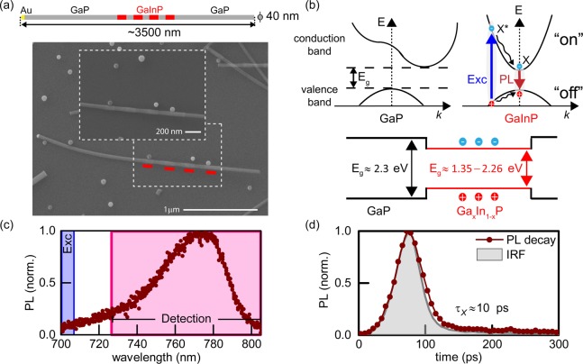
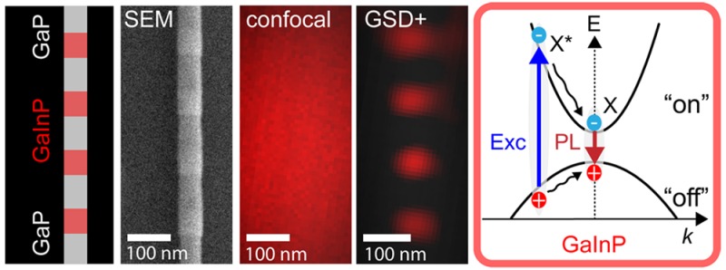
We sought to explore the intrinsic photoluminescence (PL) of nanowire axial heterostructures with the goal of improving the resolution for this class of emitter. The nanowires consisted of alternating non-luminescent gallium phosphide (GaP) and luminescent gallium indium phosphide (GaInP) segments (“barcodes”) (Figure 1a). They were synthesized by metal organic vapor phase epitaxy (MOVPE) growth, similarly to previous experiments.22 The details of the synthesis are described in the Supporting Information. In previous experiments, no emission from GaP was observed, which can be explained by the fact that, typically, GaP has an indirect bandgap (∼2.3 eV). A GaxIn1–xP alloy has a direct and tunable bandgap over a wide range of compositions (∼1.35–2.26 eV), which can be controlled during the growth procedure. Upon illumination, valence band electrons are excited to the conduction band by any photons with energy greater than the bandgap energy, and recombination of electron–hole pairs (excitons) results in bright, stable, and spectrally broad PL at room temperature (Figure 1b,c). The detected emission has typically a lifetime of τX ∼ 10–100 ps (Figure 1d).
Figure 1.
Properties of heterostructured nanowires. (a) Schematic drawing of a barcode nanowire and SEM image. Red lines indicate the photoluminescent GaInP segments. (b) Band structure diagram for GaP and GaInP. (c) Photoluminescence spectrum of a single NW GaInP segment. (d) Photoluminescence lifetime measured at room temperature with instrument response function (IRF, τjitter = 40 ps) shown in gray. The estimated photoluminescence lifetime after deconvolution was τX ≈ 10 ps.
Most popular far-field nanoscopy methods are not readily applicable to semiconductor nanowires. The coordinate-stochastic approaches (e.g., PALM26,27/STORM28), which rely on temporal signal intermittencies (blinking) of individual emitters, cannot be applied to the NWs due to the constant background PL contributions from many excitons within an extended segment. Alternatively, inhibiting short-lifetime photoluminescence by a coordinate-targeted strategy like STED29 is challenged by unwanted absorption of the de-excitation light. Thus, as NWs feature high photostability, a different strategy appeared promising: to control the transfer of electrons to the conduction band (“on” state, Figure 1b) in a coordinate-targeted manner, transferring electrons out of the valence band “off” state, as originally suggested in the classic ground state depletion (GSD) concept30−32 and later also used in saturated structured illumination microscopy (SSIM).33,34 The majority of carriers are thus forced to reside most of the time in the “on” state by using an excitation intensity distribution in the focal plane featuring one or even many zeros. Upon scanning, this leads to the acquisition of a “negative” image with subdiffraction resolution. Excitation and photoluminescence are ideally disallowed at the zero(s), that is, the targeted coordinate(s). Everywhere else, the transition out of the ground state is guaranteed, and signal is generated.
Designating the two electron states as “on” and “off”,
electron transfer to the “on” state and thus photoluminescence
can be virtually guaranteed for excitation intensities I ≫  , where hν is the photon
energy, σexc is the excitation cross-section,
τX is the photoluminescence lifetime
and Is denotes a characteristic
threshold intensity at which half of the maximal PL signal η
is elicited. The estimated fraction of electrons in the “on”
state scales with I as follows:
  . The effective point
spread function (PSF), which governs resolution, can therefore be
described by
  , where I(x) is the spatial distribution of a doughnut-shaped excitation beam,
which can be approximated around the targeted coordinate as
  . In this
expression, Δd is related to the resolution
of the diffraction-limited optical system, and ζ is the relative
depth of the excitation beam minimum (ζ ≪ 1). The resolution,
defined here as the full width at half-maximum (FWHM) of the registered
intensity dip, in the GSD microscope is well approximated by
  and tends to very small values
for increasing intensity. In practice, the resolution is limited by
the material properties and the residual intensity in the doughnut
minimum (details in Supporting Information).
We found that, despite the short exciton lifetime of several
picoseconds, it is possible to shelve electrons in the “on”
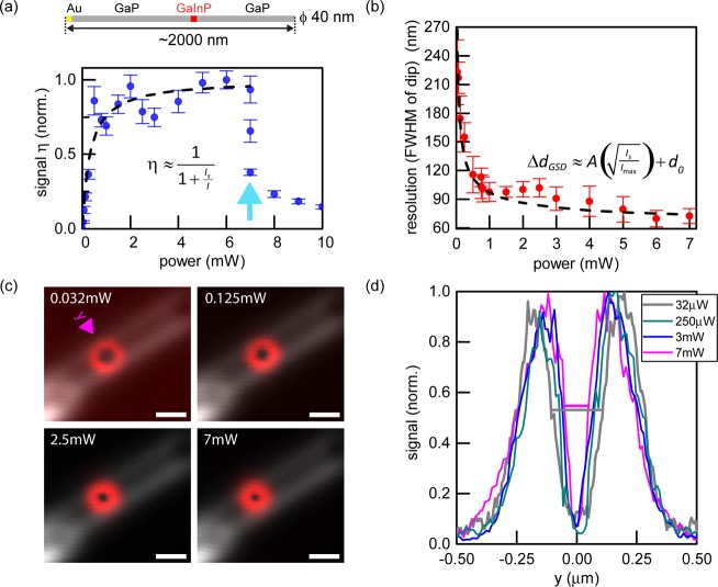
state and ensure the PL of GaInP (Figure 2a). We imaged NWs that contained a single
GaInP segment to characterize the signal η and the resolution
ΔdGSD as a function of excitation
power. All experiments were performed on a home-built GSD microscope
with short excitation pulses (∼5 ps in the focal plane) in
time-gated operation (Supporting Information). On the basis of experimental data (Figure 2a), we inferred a peak threshold intensity  . Having
identified the PL properties of GaInP (Figures 1 and 2a), the resolution
of the imaging system was significantly improved by adopting a doughnut-shaped
excitation beam (Figure 2b–d). For the excitation wavelength λ = 700 nm, the
resolution was improved to values comparable to the GaInP segment
size (∼50 nm). PL intensity profiles orthogonal to the NW axis
(Figure 2d), that is,
across the narrow dimension (labeled as y), were
used to estimate the resolution scaling with excitation power (Figure 2b,d). Note that our
measurements were carried out with a single NW width of ∼50
nm (and this offset was taken into account in the fitting analysis),
meaning that resolution will not tend to zero for very large powers.
In addition, the dip of the doughnut-shaped profile is narrower in
FWHM than a Gaussian-like standard excitation profile for the same
wavelength (compare Figures 2b and 3g). Occasionally, we observed
a permanent reduction of the PL signal (to a lower PL level, or even
complete loss of signal) starting at powers of ∼3–7
mW (for example, the arrow in Figure 2a). The PL reduction was often accompanied by an increased
contrast of the registered minimum (Figure S6).
Figure 2.
Resolution increase in GSD photoluminescence nanoscopy for a nanowire with a single GaInP segment. (a) Saturation behavior of the GaInP photoluminescence signal η. The saturation power is PS = 0.322 mW (corresponding to a peak threshold intensity IS ≈ 400 MW/cm2). The blue arrow indicates abrupt, irreversible decreases in photoluminescence with three subsequent measurements at 7 mW shown. Error bars indicate standard deviations of maximal signal from several adjacent line profiles. (b) Resolution scaling ΔdGSD as a function of the excitation power. The resolution was defined as the full width at half-maximum (FWHM) of the signal dip. Experimental data and fits to the shown expressions are displayed in (a) and (b) (including a finite offset related to the physical segment diameter in b). Error bars indicate standard deviations from several adjacent line profiles. (c) Scattering (gray) and photoluminescence (red) signal from a single NW. Scale bars: 500 nm. (d) Photoluminescence intensity profiles showing resolution changes as a function of the excitation power.
Figure 3.
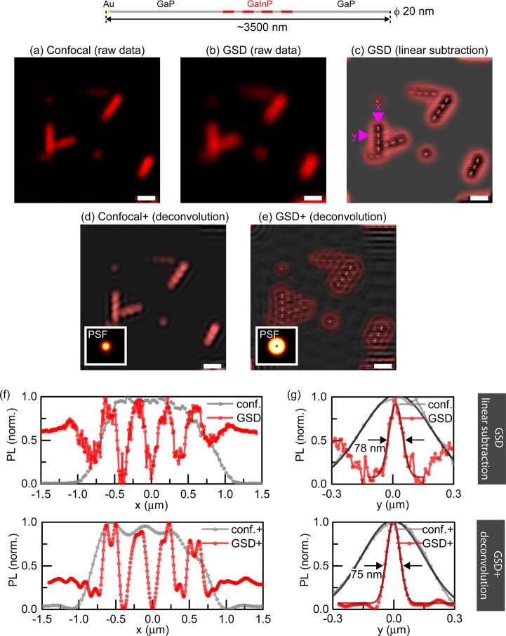
Photoluminescence nanoscopy of barcode nanowires (ϕ = 20 nm) with long photoluminescent segments. (a) Nanowires imaged in confocal mode with an excitation wavelength of λ = 700 nm (b) The same nanowires imaged with GSD PL nanoscopy (excitation power 5 mW, excitation wavelength λ = 700 nm). (c) Restored image by subtraction of raw-data GSD image from its low-frequency counterpart (not shown). (d,e) Reconstructed confocal (d) and GSD (e) image by Wiener deconvolution algorithm with PSFs (insets) calculated analytically. (f,g) PL intensity line profiles along (x) and across (y) a NW to compare confocal and GSD images for (a,c) (top) and (d,e) (bottom), showing the resolution improvement in GSD nanoscopy. All scale bars: 1 μm.
Next, we proceeded to explore the imaging of barcode NWs22 (Figures 3–5). We imaged NWs that were synthesized to have a diameter of ∼20 nm and consisted of four GaInP PL segments (233 ± 40 nm length) separated by nonluminescent GaP segments (164 ± 21 nm), as characterized by SEM. Figure 3a–c provides example confocal and GSD image comparisons. The confocal microscopy mode (Figure 3a) did not resolve individual segments, even after the application of deconvolution algorithms incorporating the known PSF (Figure 3d). GSD nanoscopy (Figure 3b,c,e) clearly distinguished the four segments. We retrieved a more intuitive image representation (Figure 3c) by simple subtraction of the raw data from its low-frequency counterpart (obtained by low-pass filtering in the frequency domain to remove high-resolution information; see Supporting Information). In principle, the corresponding confocal data can also be used to provide the reference image for subtraction. On the basis of this image (Figure 3c), the lengths of the GaP and GaInP segments appeared as 162 ± 20 nm and 225 ± 11 nm, respectively, in an intensity profile along the NW axis (Figure 3f, direction labeled x; lengths were measured as FWHMs based on spacings of maxima and minima; standard deviations from n = 12 and 9 segments, respectively). Providing a convenient target to estimate the resolution on the thinnest spatial feature, the intensity profile across the NW, that is, orthogonal to the NW axis (Figure 3g, direction labeled y) was reduced from 388 ± 25 nm in confocal mode to 76 ± 11 nm in GSD (n = 12). The inferred resolution enhancement by 5-fold therefore closely matches the modeled PSF of ∼66 nm at 5 mW (details in Supporting Information section “Limitations of direct subdiffraction imaging with GSD”).
Figure 5.
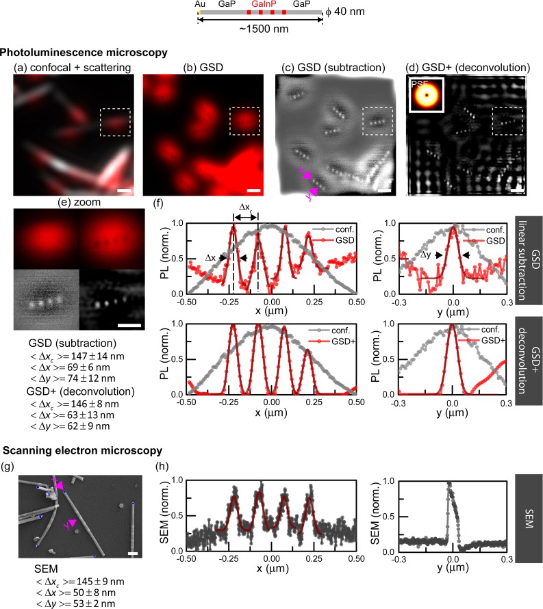
Photoluminescence nanoscopy of barcode nanowires (ϕ = 40 nm) with short luminescent segments and larger spacers compared to NWs in Figure 4 to increase the contrast. (a) Nanowires imaged in confocal mode (excitation wavelength λ = 700 nm). (b) The same area imaged by GSD PL nanoscopy (excitation power, 5 mW). (c) Restored image by linear subtraction. (d) Deconvolved GSD image by Wiener deconvolution. The inset shows the PSF. (e) Enlarged view of selected image regions from (a–d). (f) Intensity profile lines along (x) and across (y) the NW indicated by pink arrows in (c). (g) Nanowires imaged by scanning electron microscopy (SEM). (h) Intensity profile lines along (x) and across (y) the NW indicated by pink arrows in (g). Symbols: Δxc, separation of adjacent maxima; Δx, length of segment; Δy, width of segment. Data tabulated in the bottom left margin compare GSD and SEM results for NWs from the same batch for more than seven segments. Scale bars 500 nm (a–d), 200 nm (e,g).
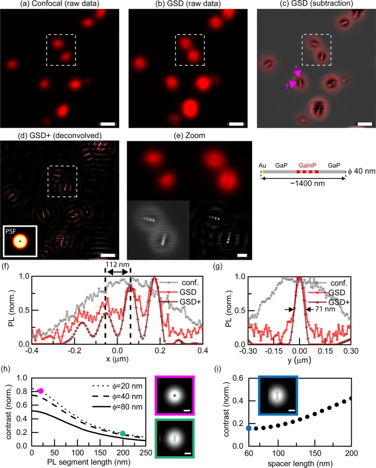
Moving to shorter and more closely spaced GaInP segments (Figure 4), we imaged NWs whose segment dimensions were characterized using SEM to 64 ± 15 nm/50 ± 20 nm for GaInP/GaP lengths, respectively, with a diameter ϕ = 43 ± 3 nm (Supporting Information, “Specification of NWs” section). The relatively large uncertainties for the segment length measurements are due to low contrast between GaP/GaInP segments in SEM images, as well as possible differences across the population of NWs related to the growth procedure. GSD nanoscopy resolved individual luminescent segments (Figure 4b–d) with an average separation of their centers of 112 ± 13 nm (n = 20 segments; SEM, 114 ± 5 nm n = 32 segments). Post-deconvolution (Figure 4d,f), we characterized the segment lengths to be 66 ± 10 nm/50 ± 16 nm (GaInP/GaP, n ≥ 15), observing an excellent agreement with the SEM measurements. While contrast was high (>0.8) for an isolated segment (Figure 2c,d), multiple closely spaced segments were imaged at significantly reduced contrast (<0.22). For the nanowires of Figure 4, we found that the contrast continuously decreased between adjacent GaInP segments along a nanowire (compare enlarged views in Figure 4e), possibly related to a gradation in inherent photoluminescence strength.35 The GaInP segment with the lowest photoluminescence corresponds to the first grown segment.22 Moreover, in GaInP nanowires, reduced contrast can arise from differences in material composition along the length of the nanowires, which affect the intensity, as previously described.22,36
Figure 4.
Photoluminescence nanoscopy of barcode nanowires (ϕ = 40 nm) with short luminescent segments. (a) Nanowires imaged in confocal mode. Excitation wavelength λ = 700 nm. (b) The same area imaged by GSD PL nanoscopy with excitation power 3 mW. (c) Restored image by subtraction of raw-data GSD image from its low-frequency counterpart (not shown). (d) Reconstructed GSD image by Wiener deconvolution algorithm with PSF (inset) calculated analytically. (e) Enlarged views of selected image regions from (a–d) (GSD subtraction and deconvolved shown in greyscale for better visualization of achieved contrast). (f,g) Intensity profile lines along (x) and across (y) a NW indicated by pink arrows. (h) Simulated contrast for GSD imaging of an extended PL segment versus photoluminescence segment length (for different NW diameters ϕ). (i) Simulated imaging contrast dependence on separation between luminescent segments (at the middle segment). The modeled NW consists of three photoluminescence segments with diameter and length equal 20 nm. Images in (h,i) show the images calculated as a convolution of the objects (red) with the modeled PSF for 5 mW excitation power. Scale bars 1 μm (a–d), 200 nm (e,h,i).
Modeling of the GSD image formation revealed a clear connection of image contrast with the PL segment length and diameter (Figure 4h), with highest contrasts for shortest and thinnest PL segments. In addition, small spacings between segments lead to decreased contrast (Figure 4i). Therefore, the observed contrast enhancement upon the sudden decrease in PL signal (Figure S6) suggests a volume reduction of the emissive GaInP segment. As size and spacing strongly affect contrast, there is clearly room for optimization in the design of heterostructures to increase the quality of images, keeping in mind that smaller PL volumes come with reduced signals. Figure 5 displays further data on 40 nm diameter NWs with short luminescent segments (50 ± 8 nm), this time with ∼2 times longer GaP spacers (95 ± 13 nm). The contrast along the NWs increased from 0.10 for the nanowires in Figure 4 to 0.14 for the nanowires in Figure 5 (data not shown). We compared the GSD nanoscopy characterization of the nanowires to SEM images (Figure 5c–h) and found an excellent agreement in the segment diameters ⟨Δy⟩, lengths ⟨Δx⟩, and separations ⟨Δxc⟩, extracted using both methods (data tabulated in Figure 5).
In summary, we have demonstrated experimentally that GSD nanoscopy resolves GaP/GaInP NW heterostructures with diameters down to 20 nm at a 5-fold resolution enhancement compared to confocal microscopy. GaP/GaInP NWs with even smaller diameters (10 nm) became challenging to image due to significant emission intermittency. As the diameter of NWs approached the exciton size (GaInP ∼4–10 nm), the PL showed strong fluctuations (Figure S5 in Supporting Information), making segment positions virtually impossible to extract. We note that PL fluctuations can be possibly controlled37,38 by choosing the PL material, notably through exciton-size or core–shell engineering to protect surface excitons. However, the nature of signal intermittencies would not allow the direct application of a PALM/STORM/GSDIM strategy:26−28,39 Excitons from an individual segment cannot be made to emit together while keeping the neighboring segment “silent”, because the electrons behave independently and cannot be “locked” into one of the two states for an extended time. Even if selection (“activation”) at the single-exciton level were realized (e.g., by very low fluxes of excitation photons), the exciton would not deliver bursts of ≫1 consecutive photons, which is a fundamental requirement to allow the localization of one entity (here, the segment).
Further, it is worth commenting on a relevant difference between methods that prepare the “on” state at the targeted coordinate(s) (“positive” imaging) and those “inverted” approaches, as applied here, which locally single out the “off” state (“negative” imaging). In both cases, coordinates are targeted by positioning a zero or zeros (minimum/a) of the state-switching light intensity. In “positive” imaging, signals from the locally prepared “on”-state features are not affected by any contributions from neighboring non-targeted features because these are in an “off” state. But the “negative”-imaging modalities, forcing the emissive “on” state everywhere except at the zero(s), suffer from the problem of collecting signal from the entire diffraction zone. This includes contributions from all nearby features, whose signals fill up the all-important dip in registered intensity, partially hampering super-resolution information in the presence of noise. Note that the limitation does not stem from an imperfect state preparation. The “negative” modality is just as efficient in generating the “on”–“off” state contrast in the specimen as the “positive” modality, but the readout/detection step is less favorable in terms of contrast. The effect of reduced contrast in the presence of nearby emitters was previously appreciable in GSD nanoscopy data recorded from nitrogen vacancy (NV) color centers, that is, confined point-like emitters in diamond.32 In the extended semiconductor structures investigated here, we showed that shorter PL segments lead to higher contrast, as do larger separations from the nearest luminescent neighbors. Certainly, the ability to freely control the geometry within NW heterostructures (notably, the sequence of PL segment lengths and spacings) allows for further optimization. Another possible direction for improvements will be controlled changes in the NW segments’ material composition. This would allow for the modification of spectral characteristics (even customized differences among adjacent PL segments) as well as saturation behaviors and damage thresholds. The latter remains a limiting factor to additional resolution improvements, and a better understanding of the mechanisms of PL loss will benefit further advances.
Because of the far-red excitation wavelength (low phototoxicity) and the moderate average power, we believe the described approach will be highly relevant for revealing positions, orientations, and identities of NWs in biological contexts. Membranes or other cellular structures could be visualized by complementary nanoscale imaging methods such as STED. The good performance of NW GSD nanoscopy at room temperature indicates similar applicability at physiological temperatures under live-cell conditions. The comparatively low excitation power required to obtain a substantial resolution enhancement over confocal imaging should allow parallelization of this approach, which may significantly increase the speed of nanoscale imaging in the future.
Glossary
ABBREVIATIONS
- GaInP
gallium indium phosphide
- GaP
gallium phosphide
- GSD
ground state depletion
- NW
nanowire
- NV
nitrogen vacancy
- PL
photoluminescence
- PSF
point spread function
- SEM
scanning electron microscopy
- STED
stimulated emission depletion
- QD
quantum dot
Supporting Information Available
The Supporting Information is available free of charge on the ACS Publications website at DOI: 10.1021/acs.nanolett.7b00468.
Experimental setup, synthesis of GaP/GaInP barcode nanowires, sample preparation, mathematical image processing, limitations of direct subdiffraction imaging with GSD (resolution and contrast), specifications of NWs, lookup tables (color scales) (PDF)
Author Contributions
The manuscript was written through contributions of all authors. All authors have given approval to the final version of the manuscript.
This work was supported by the Foundation for Polish Science International Ph.D. Projects Programme, cofinanced by the EU European Regional Development Fund. The Lund team acknowledges funding from NanoLund, the Swedish Research Council (VR) and the ERC consolidator grant NanoPokers (682206) and thank Nicklas Anttu for help with nanowire characterization.
The authors declare no competing financial interest.
Supplementary Material
References
- Tian B.; Cohen-Karni T.; Qing Q.; Duan X.; Xie P.; Lieber C. M. Science 2010, 329, 830–834. 10.1126/science.1192033. [DOI] [PMC free article] [PubMed] [Google Scholar]
- Qing Q.; Jiang Z.; Xu L.; Gao R.; Mai L.; Lieber C. M. Nat. Nanotechnol. 2013, 9 (2), 142–147. 10.1038/nnano.2013.273. [DOI] [PMC free article] [PubMed] [Google Scholar]
- Eschermann J. F.; Stockmann R.; Hueske M.; Vu X. T.; Ingebrandt S.; Offenhäusser A. Appl. Phys. Lett. 2009, 95 (8), 083703. 10.1063/1.3194138. [DOI] [Google Scholar]
- Liu H.; He J.; Tang J.; Liu H.; Pang P.; Cao D.; Krstic P.; Joseph S.; Lindsay S.; Nuckolls C. Science 2010, 327 (5961), 64–67. 10.1126/science.1181799. [DOI] [PMC free article] [PubMed] [Google Scholar]
- Williams K. A.; Veenhuizen P. T. M.; de la Torre B. G.; Eritja R.; Dekker C. Nature 2002, 420 (6917), 761–761. 10.1038/420761a. [DOI] [PubMed] [Google Scholar]
- Bisker G.; Dong J.; Park H. D.; Iverson N. M.; Ahn J.; Nelson J. T.; Landry M. P.; Kruss S.; Strano M. S. Nat. Commun. 2016, 7, 10241. 10.1038/ncomms10241. [DOI] [PMC free article] [PubMed] [Google Scholar]
- Patolsky F.; Timko B. P.; Yu G.; Fang Y.; Greytak A. B.; Zheng G.; Lieber C. M. Science 2006, 313 (5790), 1100–1104. 10.1126/science.1128640. [DOI] [PubMed] [Google Scholar]
- Robinson J. T.; Jorgolli M.; Shalek A. K.; Yoon M.-H.; Gertner R. S.; Park H. Nat. Nanotechnol. 2012, 7 (3), 180–184. 10.1038/nnano.2011.249. [DOI] [PMC free article] [PubMed] [Google Scholar]
- Fakhri N.; Wessel A. D.; Willms C.; Pasquali M.; Klopfenstein D. R.; MacKintosh F. C.; Schmidt C. F. Science 2014, 344 (6187), 1031–1035. 10.1126/science.1250170. [DOI] [PubMed] [Google Scholar]
- Smith B. R.; Ghosn E. E. B.; Rallapalli H.; Prescher J. A.; Larson T.; Herzenberg L. A.; Gambhir S. S. Nat. Nanotechnol. 2014, 9 (6), 481–487. 10.1038/nnano.2014.62. [DOI] [PMC free article] [PubMed] [Google Scholar]
- Xu A. M.; Aalipour A.; Leal-Ortiz S.; Mekhdjian A. H.; Xie X.; Dunn A. R.; Garner C. C.; Melosh N. A. Nat. Commun. 2014, 5, 3613. 10.1038/ncomms4613. [DOI] [PMC free article] [PubMed] [Google Scholar]
- Hällström W.; Lexholm M.; Suyatin D. B.; Hammarin G.; Hessman D.; Samuelson L.; Montelius L.; Kanje M.; Prinz C. N. Nano Lett. 2010, 10 (3), 782–787. 10.1021/nl902675h. [DOI] [PubMed] [Google Scholar]
- Cellot G.; Cilia E.; Cipollone S.; Rancic V.; Sucapane A.; Giordani S.; Gambazzi L.; Markram H.; Grandolfo M.; Scaini D.; Gelain F.; Casalis L.; Prato M.; Giugliano M.; Ballerini L. Nat. Nanotechnol. 2009, 4 (2), 126–133. 10.1038/nnano.2008.374. [DOI] [PubMed] [Google Scholar]
- Piret G.; Perez M.-T.; Prinz C. N. ACS Appl. Mater. Interfaces 2015, 7 (34), 18944–18948. 10.1021/acsami.5b03798. [DOI] [PubMed] [Google Scholar]
- Prinz C. N. J. Phys.: Condens. Matter 2015, 27 (23), 233103. 10.1088/0953-8984/27/23/233103. [DOI] [PubMed] [Google Scholar]
- Persson H.; Li Z.; Tegenfeldt J. O.; Oredsson S.; Prinz C. N. Sci. Rep. 2015, 5, 18535. 10.1038/srep18535. [DOI] [PMC free article] [PubMed] [Google Scholar]
- Kim W.; Ng J. K.; Kunitake M. E.; Conklin B. R.; Yang P. J. Am. Chem. Soc. 2007, 129 (23), 7228–7229. 10.1021/ja071456k. [DOI] [PubMed] [Google Scholar]
- Berthing T.; Bonde S.; Sørensen C. B.; Utko P.; Nygård J.; Martinez K. L. Small 2011, 7 (5), 640–647. 10.1002/smll.201001642. [DOI] [PubMed] [Google Scholar]
- Shalek A. K.; Robinson J. T.; Karp E. S.; Lee J. S.; Ahn D.-R.; Yoon M.-H.; Sutton A.; Jorgolli M.; Gertner R. S.; Gujral T. S.; MacBeath G.; Yang E. G.; Park H. Proc. Natl. Acad. Sci. U. S. A. 2010, 107 (5), 1870–1875. 10.1073/pnas.0909350107. [DOI] [PMC free article] [PubMed] [Google Scholar]
- Mumm F.; Beckwith K. M.; Bonde S.; Martinez K. L.; Sikorski P. Small 2013, 9 (2), 263–272. 10.1002/smll.201201314. [DOI] [PubMed] [Google Scholar]
- Berthing T.; Bonde S.; Rostgaard K. R.; Madsen M. H.; Sørensen C. B.; Nygård J.; Martinez K. L. Nanotechnology 2012, 23 (41), 415102. 10.1088/0957-4484/23/41/415102. [DOI] [PubMed] [Google Scholar]
- Adolfsson K.; Persson H.; Wallentin J.; Oredsson S.; Samuelson L.; Tegenfeldt J. O.; Borgström M. T.; Prinz C. N. Nano Lett. 2013, 13 (10), 4728–4732. 10.1021/nl4022754. [DOI] [PubMed] [Google Scholar]
- Mattsson K.; Adolfsson K.; Ekvall M. T.; Borgström M. T.; Linse S.; Hansson L.-A.; Cedervall T.; Prinz C. N. Nanotoxicology 2016, 10 (8), 1160–1167. 10.1080/17435390.2016.1189615. [DOI] [PMC free article] [PubMed] [Google Scholar]
- Hell S. W. Science 2007, 316 (5828), 1153–1158. 10.1126/science.1137395. [DOI] [PubMed] [Google Scholar]
- Huang B.; Babcock H.; Zhuang X. Cell 2010, 143 (7), 1047–1058. 10.1016/j.cell.2010.12.002. [DOI] [PMC free article] [PubMed] [Google Scholar]
- Betzig E.; Patterson G. H.; Sougrat R.; Lindwasser O. W.; Olenych S.; Bonifacino J. S.; Davidson M. W.; Lippincott-Schwartz J.; Hess H. F. Science 2006, 313 (5793), 1642–1645. 10.1126/science.1127344. [DOI] [PubMed] [Google Scholar]
- Hess S. T.; Girirajan T. P. K.; Mason M. D. Biophys. J. 2006, 91 (11), 4258–4272. 10.1529/biophysj.106.091116. [DOI] [PMC free article] [PubMed] [Google Scholar]
- Rust M. J.; Bates M.; Zhuang X. Nat. Methods 2006, 3 (10), 793–796. 10.1038/nmeth929. [DOI] [PMC free article] [PubMed] [Google Scholar]
- Hell S. W.; Wichmann J. Opt. Lett. 1994, 19 (11), 780–782. 10.1364/OL.19.000780. [DOI] [PubMed] [Google Scholar]
- Hell S. W.; Kroug M. Appl. Phys. B: Lasers Opt. 1995, 60 (5), 495–497. 10.1007/BF01081333. [DOI] [Google Scholar]
- Bretschneider S.; Eggeling C.; Hell S. W. Phys. Rev. Lett. 2007, 98 (21), 218103. 10.1103/PhysRevLett.98.218103. [DOI] [PubMed] [Google Scholar]
- Rittweger E.; Wildanger D.; Hell S. W. EPL 2009, 86 (1), 14001. 10.1209/0295-5075/86/14001. [DOI] [Google Scholar]
- Heintzmann R.; Jovin T. M.; Cremer C. J. Opt. Soc. Am. A 2002, 19 (8), 1599–1609. 10.1364/JOSAA.19.001599. [DOI] [PubMed] [Google Scholar]
- Gustafsson M. G. L. Proc. Natl. Acad. Sci. U. S. A. 2005, 102 (37), 13081–13086. 10.1073/pnas.0406877102. [DOI] [PMC free article] [PubMed] [Google Scholar]
- Bao W.; Melli M.; Caselli N.; Riboli F.; Wiersma D. S.; Staffaroni M.; Choo H.; Ogletree D. F.; Aloni S.; Bokor J.; Cabrini S.; Intonti F.; Salmeron M. B.; Yablonovitch E.; Schuck P. J.; Weber-Bargioni A. Science 2012, 338 (6112), 1317–1321. 10.1126/science.1227977. [DOI] [PubMed] [Google Scholar]
- Berg A.; Lenrick F.; Vainorius N.; Beech J. P.; Wallenberg R. L.; Borgström M. T. Nanotechnology 2015, 26 (43), 435601. 10.1088/0957-4484/26/43/435601. [DOI] [PubMed] [Google Scholar]
- Frantsuzov P.; Kuno M.; Janko B.; Marcus R. A. Nat. Phys. 2008, 4 (5), 519–522. 10.1038/nphys1001. [DOI] [Google Scholar]
- Glennon J. J.; Tang R.; Buhro W. E.; Loomis R. A. Nano Lett. 2007, 7 (11), 3290–3295. 10.1021/nl0714583. [DOI] [PubMed] [Google Scholar]
- Fölling J.; Bossi M.; Bock H.; Medda R.; Wurm C. A.; Hein B.; Jakobs S.; Eggeling C.; Hell S. W. Nat. Methods 2008, 5 (11), 943–945. 10.1038/nmeth.1257. [DOI] [PubMed] [Google Scholar]
Associated Data
This section collects any data citations, data availability statements, or supplementary materials included in this article.


