Abstract
Processes of holographic recording of surface relief structures using As2S3:Mn–Se multilayer nanostructures as registering media were studied in this paper. Optical properties of As2S3:Mn, Se layers, and As2S3:Mn–Se multilayer nanostructures were investigated. Values of optical bandgaps were obtained from Tauc dependencies. Surface relief diffraction gratings were recorded. Direct one-stage formation of surface relief using multilayer nanostructures is considered. For the first time, possibility of direct formation of magnetic relief simultaneous with surface relief formation under optical recording using As2S3:Mn–Se multilayer nanostructures is shown.
Keywords: Multilayer nanostructures, Diffraction gratings, Magnetic relief, Chalcogenide glasses, Direct recording
Background
Chalcogenide glasses (ChGs) are typical representatives of non-oxide glasses. ChGs are very promising versatile functional materials for use in optoelectronics as high-speed optical elements, for applications such as data processing devices, electronic switches, and other optical elements. ChGs possess unique characteristics which are different from other glasses: photoinduced phenomena, broad optical transmission window, high linear refractive index (n ≈ 2–3), and high optical non-linearity (around two orders of magnitude higher than silica, this makes them suitable for ultra-fast switching in telecommunication systems). These materials and their properties were reviewed in a number of books and review papers [1–6]. ChGs transmit to longer wavelengths in the IR than silica and fluoride glasses. ChGs based on sulfur, selenium, and tellurium typically transmit up to around 10, 15, and 20 μm, respectively [5]. In spite of a wide range of compositions in binary, ternary, and more complex systems of chalcogenide glasses, the problem of modification of parameters still exists. Such modifications can be performed partially by the special technologies (cooling rate, thin film deposition, exposure by light, e-beams or ion beams), by modification, or by creating complex artificial structures [7–13].
The properties of ChGs can be changed by doping with transitional metals or rare-earth elements resulting in change of thermal, optical, luminescent, and magnetic properties [14, 15]. Also the properties of ChGs can be changed by external light-, electron-, or ion-beam source resulting in change of refractive index, optical transmittance, volume (thickness), and viscosity [6, 16, 17]. Based on the changes of these parameters, different optical elements (lenses, gratings, beam splitters, waveguides, etc.) on micro/nanoscale can be fabricated by laser/electron- irradiation directly or followed by chemical development [6].
Composite nanomultilayer structures on the base of chalcogenide glasses are particularly interesting because they enable to realize one-step direct recording of surface relief without selective etching [18–28]. Multilayer structures are the simplest artificial nanostructures which can be rather easily produced with controlled geometrical parameters and investigated as thin films. It is essential, since the changes of the optical parameters (blue shift of the fundamental absorption edge, quantum states, luminescence), as well as of the conductivity and melting temperature (stability), are characteristic and usually examined in nanostructures. A lot of efforts were made to find classic quantum effects, to influence the structure, stability, and thermodynamic parameters of the chalcogenide material in very thin layers (see for example a review of Tanaka [16]), but the obtained results up to now are mostly connected to the optical recording. In this paper, results of direct surface and magnetic relief recording using As2S3:Mn 2 wt.%–Se nanostructures are considered.
Methods
The As2S3 glasses with manganese concentration 2 wt.% were prepared by standard melt-quenching technique using constituent elements of 6 N purity in vacuum-sealed silica ampoules. Ampoules were heated at 80 K/h rate, melt was held at 1010 K during 80 h with subsequent quenching in the air at 10 K/h rate.
Composite nanomultilayer structures on the base of chalcogenide glasses were prepared by co-condensation in vacuum. The scheme of the experimental setup is shown in Fig. 1.
Fig. 1.
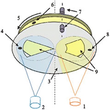
Scheme of device for fabrication of multilayer nanocomposites on the base of chalcogenide glasses. (1) As2S3:Mn evaporator, (2) evaporator of Se, (3) stationary mask, (4), (8) quartz thickness sensors fixed on mask, (5) rotating sample holder, (6) quartz thickness sensor fixed on rotating sample holder, (7) optical fibers of the spectrophotometer, (9) windows in mask
Scheme of samples cross section is shown in Fig. 2.
Fig. 2.
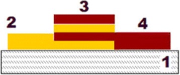
Sample scheme: 1—glass substrate; 2—As2S3:Mn 2 wt.% layer by layer; 3—As2S3:Mn 2 wt.%/Se nanostructure; 4—Se layer by layer
The overlapping part of samples (Fig. 2) contains alternating nanolayers of Se and As2S3:Mn 2 wt.%, i.e., two wide rings overlap in the central part of the substrate-forming nanostructure. Outside and internal rings of layers on the substrate contain pure compositions of Se and As2S3:Mn 2 wt.%, respectively.
We obtained the layers of Se and As2S3:Mn at the same time on the same substrate consequently through the windows in mask, and they were used to check the composition and calculate the ratio of the layer thicknesses in one modulation period N (the total thickness of one Se and As2S3:Mn nanolayers). Modulation period was ~21 nm = 10 nm + 11 nm; number of periods 90; thickness of one As2S3:Mn 2% layer d ≈ 11 nm; thickness of one Se layer d ≈ 10 nm; and total structure thickness ~2000 nm.
The amorphous nature of the samples was verified at room temperature by X-ray diffraction (XRD) technique using a ARL X’tra (Thermo Scientific) diffractometer equipped with a copper tube. The voltage on the tube amounted to 45 kV and current 30 mA. The scattering intensities were measured over an angular range of 2° ≤ θ ≤ 140° with a step size of Δ(θ) = 0.2° and a count time of 5 s per step.
Obtained films and composite nanomultilayer structures on the base of chalcogenide glasses were investigated using UV–vis spectroscopy. Transmission spectra were obtained in the region 200–900 nm with the use of a spectrophotometer Specord M40.
Morphology of the obtained films and surface relief of the obtained gratings were studied by atomic force microscopy (AFM) with the use of a Nanoscope-IIIa AFM.
Magnetizations of samples were measured with a Cryogenic S600 Super-conducting Quantum Interference Device (SQUID) magnetometer in the temperature range of 3–300 K and in the magnetic field up to 6 T. Measurements of magnetic properties (temperature dependence of the specific magnetic moment) were performed under the different conditions of samples cooling. The sample was cooled in a zero external magnetic field, and then the setting of the magnetic field with specified magnitude was performed. In the following, the magnetic field was remained constant during the sample heating. The interval of temperature change was chosen in such a way that the maximal value of temperature exceeded the temperature of transition into the paramagnetic state. Such dependencies in the following are denoted as ZFC [15]. Further, a sample was cooled in the magnetic field and M = M(T) was obtained, such regime was denoted as FC [15].
Diffraction gratings with 1- and 1.5-μm period were recorded by two laser beams using different light polarization with synchronous diffraction efficiency measurement by red laser (λ = 650 nm) in the first diffraction order. Monomode diode-pumped solid state (DPSS) green laser (λ = 532 nm) with average spot power density from 150 up to 350 mW/cm2 was used.
Local magnetic properties of the surface relief gratings which were fabricated using As2S3:Mn–Se multilayer nanostructures were investigated using gradient magnetic force microscopy (MFM). MFM measurements were carried out using a scanning probe microscope NanoScope IIIa Dimension 3000 with the use of a two-scan method.
Results and Discussion
X-ray diffraction patterns confirm the amorphous nature of the bulk samples of chalcogenide glasses (Fig. 3). Spectra are shifted on some distance for better observation. Calculated radial distribution functions have shown no significant change with the introduction of manganese (Fig. 4).
Fig. 3.
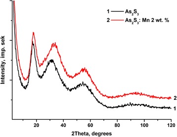
X-ray diffraction patterns for As2S3 (1) and As2S3:Mn glasses (2)
Fig. 4.
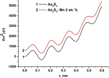
Radial distribution functions for As2S3 (1) and As2S3:Mn 2% glasses (2)
Magnetic Properties
ChGs are diamagnetics, in particular As2S3 glass. Introduction of Mn dopant changes magnetic properties of glasses. Thus, in constant magnetic field dependence of mass magnetization M = M(T) is observed which is characteristic for paramagnetics and ferromagnetics in paramagnetic region of temperature (Fig. 5) and described by Curie–Weiss law.
Fig. 5.
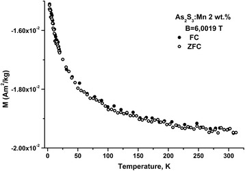
Dependence of mass magnetization M on temperature for As2S3:Mn
Optical Properties
Transmission spectra of As2S3:Mn 2 wt.% layers, Se layers, and As2S3:Mn 2 wt.%/Se multilayer structures are shown in Fig. 6.
Fig. 6.
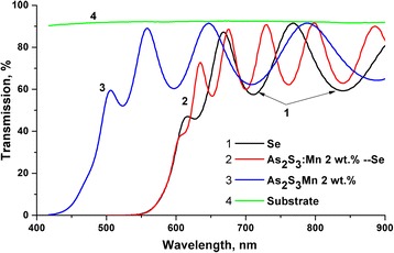
Transmission spectra of As2S3:Mn 2 wt.% layers, Se layers, and As2S3:Mn 2 wt.%/Se multilayer structure
Optical constants of layers were obtained from transmission spectra using Swanepoel method [29] and analyzed within the frames of a single oscillator model. The absorption edge was determined by the relation α × hν = const (hν − E g)2, where hν is the energy of light quantum, E g—optical bandgap, and α—absorption coefficient. E g values were as follows: Se—1.93 eV, As2S3:Mn 2 wt.%—2.32 eV, composite As2S3:Mn 2 wt.%/Se layer—1.94 eV. Absorption edge of the multilayer structure As2S3:Mn 2%/Se is close to the absorption edge of the optical gap of the Se layer (see Fig. 6).
Optical properties were analyzed within the frame of a single oscillator model [29]. According to this model, refractive index n is related to energy of incident photon E by equation n 2 − 1 = E d E 0/E 0 2 − E 2 where E 0 is single oscillator energy and E d is dispersion energy.
In this expression E 0 determines the position of the effective oscillator connected with an average energy gap and E d is dispersion energy characterizing the strength of interband transitions. E 0 and E d values were obtained from plots (n 2 − 1)−1 = f(E 2) using least squares fitting method to straight line. Parameters of the single oscillator model for As2S3 Mn 2 wt.% and Se layers, and As2S3:Mn 2 wt.%/Se nanomultilayer structure were obtained from such plots together with optical bandgap values obtained using Tauc plot αhν = const (hν − E g)2 are presented in Table 1. Obtained values of optical bandgaps E g (see Table 1) for Se layers (1.93 eV) and As2S3:Mn 2 wt.%/Se nanomultilayer structures (1.94 eV) are close to each other. From Fig. 6, it can be seen also that absorption edges for Se layers and As2S3:Mn/Se nanomultilayer structure almost coincide.
Table 1.
Parameters of the single oscillator model for As2S3:Mn 2 wt.% and Se layers, and As2S3:Mn 2 wt.%–Se nanomultilayer structure
| Layer composition | n(0) | E d, eV | E 0, eV | E g, eV |
|---|---|---|---|---|
| Se | 2.284 | 15.086 | 3.577 | 1.93 |
| As2S3:Mn 2 wt.% | 2.248 | 18.696 | 4.611 | 2.32 |
| As2S3:Mn 2 wt.%–Se | 2.286 | 16.714 | 3.594 | 1.94 |
Here, it is necessary to mention that the doping of chalcogenide glasses by transitional metals and rare-earth element changes besides optical, structural, and magnetic properties also changes thermal and luminescent properties of chalcogenide glasses [15].
Holographic Grating Recording
Scheme of diffraction grating recording is shown in Fig. 7. Gratings were recorded with spatial frequency ~900 mm−1; for recording green laser wavelength, 532 nm was used; red laser wave length 650 nm was used for readout. Diffraction efficiency of recorded gratings was ~7% in transmission on 650 nm wavelength, absolute values. AFM image of recorded grating is shown in Fig. 8. It can be seen that obtained relief quality is high. Relief height is ~40 nm. Also gratings with spatial frequency ~1500 mm−1 were recorded (Fig. 9).
Fig. 7.
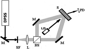
Scheme of diffraction grating recording: DPSS—laser; SF and L—collimator; BS—beam splitter; M—flat mirrors; S—registering media (sample); LD—LED; PD—registering unit
Fig. 8.
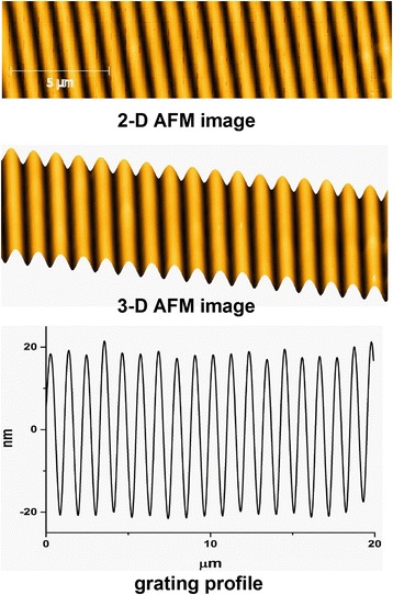
AFM image of recorded holographic grating using As2S3:Mn–Se nanomultilayers. Spatial frequency ~900 mm−1
Fig. 9.
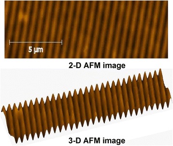
The morphology of surface diffraction gratings recorded on As2S3:Mn–Se nanomultilayers. Spatial frequency ~1500 mm−1, relief height ~26 nm
Kinetics of grating recording has shown dependence on laser beam polarization. During grating recording in such media (Fig. 10), recording process includes photostimulated changes of refractive index, volume expansion, and mass transfer. The process of grating recording using As2S3:Mn 2 wt.% layers begins right after switching on the laser illumination. A rapid increase of diffraction efficiency η of the grating is observed at the beginning of the recording process (Fig. 10, curve 4). After reaching the maximum, a η decrease of gratings follows.
Fig. 10.
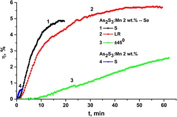
Kinetics of holographic grating recording. As2S3:Mn 2 wt.%–Se nanomultilayer structures: 1—S polarization, 2—circular polarization, 3—±45° polarization. As2S3:Mn 2 wt.% layers: 4—S polarization
The light polarizations in this experiment were to the grating vector (S polarization), the left–right circular polarization (L–R), and the linear polarization at +45° direction in one writing beam and –45° in the other one. Under the holographic recording using the two linear (S–S) polarized beams or L–R polarizations, we observed at initial stage of exposure linear dependence of η growth on time of exposure with a further stage leading to saturation (Fig. 9). The two linear polarized beams falling on the sample surface under angles of polarization (+45° to −45°) produce the linear dependence of η growth according to our measurements. Dependence of holographic grating recording on polarization of recording beams when using nanomultilayer structures on the base of chalcogenide glasses was also observed for other compositions of nanomultilayer structures [25, 27].
Interdiffusion and stress relaxation, combined with other photostimulated processes, may be involved in such expansion effects in nanomultilayer structures. The physical base of the process is considered interdiffusion of α-Se and As2S3 resulting in total volume increase in comparison with total volume of separated sublayers, and the effective intermixing of components at short, nanometer size distances. Competition between stress-induced atomic flux (towards irradiated regions of the film) and the diffusion flux induced by an increase in the bulk energy due to broken bonds (and directed from irradiated to dark regions) can result in either positive or negative net mass transfer in the irradiated region [30–34].Taking into account the change of magnetic properties of As2S3 glass after introduction of Mn, abovementioned interdiffusion and intermixing of layers and lateral diffusion in nanomultilayer structures, we expected that by using As2S3:Mn/Se nanomultilayer structures it would be possible to obtain magnetic relief (besides the surface one) during holographic grating recording.
Magnetic Relief Formation
Local magnetic properties of grating surface relief were studied using gradient magnetic force microscopy. AFM and MFM images of the recorded reliefs are shown in Fig. 11.
Fig. 11.
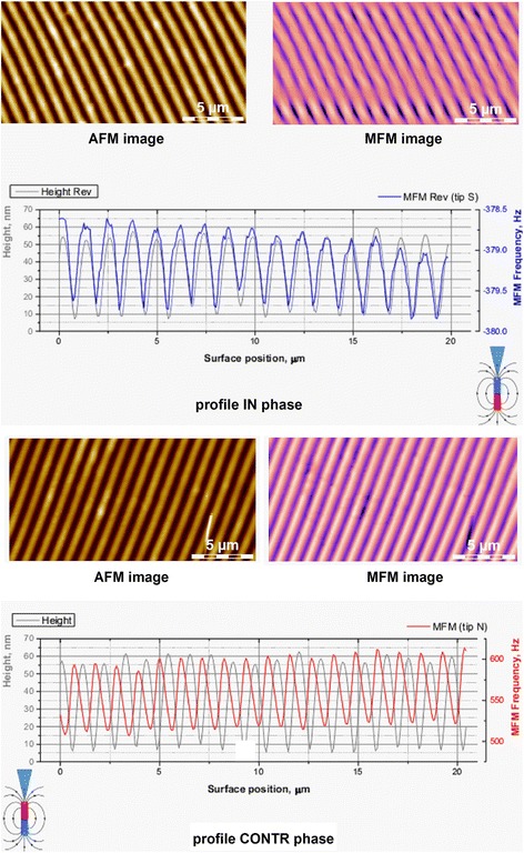
AFM image of grating surface relief and MFM image of magnetic relief for different directions of tip magnetization and also surface relief and magnetic relief profiles
MFM images show that distribution and value of magnetic field correlates with grating relief in phase or counter phase depending on the tip magnetization direction. Possibility of direct one-step magnetic relief formation during grating recording using As40S60:Mn 2 wt.%/Se nanomultilayer structures (or similar ones) can be used for creation of surface relief optical elements with unique properties and in magnetic memory applications.
Conclusions
The presented results demonstrated a direct, one-step process of holographic recording by green light beam of surface relief structures using As2S3:Mn 2 wt.%/Se nanomultilayer structures.
Due to the changes in transmission, reflection, and in thickness under the influence of laser irradiation, As40S60:Mn 2 wt.%/Se nanomultilayer structures may be used for effective amplitude-phase optical information recording, for the production of surface relief optical elements with unique properties.
For the first time, it was shown that direct one-step magnetic relief formation is possible during grating recording using As40S60:Mn 2 wt.%/Se nanomultilayer structures.
Acknowledgements
This research was partially supported by FP-7 project SECURE-R2I.
Authors’ Contributions
AS conceived of the study and participated in its design and coordination, fabrication of chalcogenide glasses, idea of magnetic relief formation, results analysis, and drafted the manuscript. EA conceived of the study and participated in its design and coordination and results analysis. OP participated in fabrication of chalcogenide glasses, nanomultilayer structures and image recording, studied optical, thermal, and magnetic properties, and participated in results analysis. AM participated in the fabrication of nanomultilayer structures, image recording, and results analysis. AP participated in the fabrication of nanomultilayer structures and image recording. GT participated in the fabrication of nanomultilayer structures. PO participated in the results analysis. PL participated in the study of magnetic properties of recorded grating surface relief. All authors read and approved the final manuscript.
Competing Interests
The authors declare that they have no competing interests.
Publisher’s Note
Springer Nature remains neutral with regard to jurisdictional claims in published maps and institutional affiliations.
References
- 1.Wang R (2014) Amorphous Chalcogenides: Advances and Applications. Pan Stanford Publishing, Singapore
- 2.Zakery A, Elliott SR (2007) Optical Nonlinearities in Chalcogenide Glasses and their Applications. doi: 10.1007/978-3-540-71068-4
- 3.Špotûk OI, Filipecki J (2003) Free volume in vitreous chalcogenide semiconductors: possibilities of positron annihilation lifetime study. Wydaw. Wyższej Szkoły Pedagogicznej, Częstochowa
- 4.Stronski AV, Vlček M. Photosensitive properties of chalcogenide vitreous semiconductors in diffractive and holographic technologies applications. J Optoelectron Adv Mater. 2002;4:699–704. [Google Scholar]
- 5.Sanghera JS, Aggarwal ID, Shaw LB, et al. Applications of chalcogenide glass optical fibers at NRL. J Optoelectron Adv Mater. 2001;3:627–640. [Google Scholar]
- 6.Stronski AV (1998) Production of metallic patterns with the help of high resolution inorganic resists. In: Microelectron. Interconnections Assem., 1st ed. Springer Netherlands, Dordrecht, pp 263–293
- 7.DeCorby RG, Nguyen HT, Dwivedi PK, Clement TJ. Planar omnidirectional reflectors in chalcogenide glass and polymer. Opt Express. 2005;13:6228–6233. doi: 10.1364/OPEX.13.006228. [DOI] [PubMed] [Google Scholar]
- 8.Clement T, Ponnampalam N, Nguyen HT, DeCorby RG. Improved omnidirectional reflectors in chalcogenide glass and polymer by using the silver doping technique. Opt Express. 2006;14:1789–1796. doi: 10.1364/OE.14.001789. [DOI] [PubMed] [Google Scholar]
- 9.Kohoutek T, Wagner T, Orava J, et al. Multilayer planar structures prepared from chalcogenide thin films of As–Se and Ge–Se systems and polymer thin films using thermal evaporation and spin-coating techniques. J Non Cryst Solids. 2008;354:529–532. doi: 10.1016/j.jnoncrysol.2007.07.057. [DOI] [Google Scholar]
- 10.Bormashenko E, Pogreb R, Pogreb Z, Sutovski S. Development of new near-infrared filters based on the “sandwich” polymer-chalcogenide glass-polymer composites. Opt Eng. 2001;40:661–662. doi: 10.1117/1.1360241. [DOI] [Google Scholar]
- 11.Martyshkin DV, Fedorov VV, Goldstein JT, Mirov SB (2011) Mid-IR lasing of Cr:ZnSe/As2S3 :As2Se3 composite materials. In: Clarkson WA, Hodgson N, Shori R (eds) Solid State Lasers XX Technol Devices. San Francisco, p 79121I
- 12.Grynko D, Stronski A, Telbiz G, et al. Nanocomposites based on chalcogenide glass semiconductor and metal phtalocyanine. Ceram Int. 2015;41:7605–7610. doi: 10.1016/j.ceramint.2015.02.085. [DOI] [Google Scholar]
- 13.Kavetskyy TS, Borc J, Kukhazh YY, Stepanov AL (2015) The Influence of Low Dose Ion-Irradiation on the Mechanical Properties of PMMA Probed by Nanoindentation. In: Nanosci. Adv CBRN Agents Detect Inf Energy Secur. Springer Netherlands, Dordrecht, pp 65–71
- 14.Iovu MS, Andriesh AM, Buzurniuc SA, Verlan VI. Optical properties of As2S3:Pr and As2Se3:Dy amorphous composites. Dig J Nanomater Biostructures. 2007;2:201–206. [Google Scholar]
- 15.Stronski A, Paiuk O, Gudymenko A, et al. Effect of doping by transitional elements on properties of chalcogenide glasses. Ceram Int. 2015;41:7543–7548. doi: 10.1016/j.ceramint.2015.02.077. [DOI] [Google Scholar]
- 16.Tanaka K (2014) Photoinduced deformations in chalcogenide glasses. In: Amorph Chalcogenides Adv Appl. Pan Stanford Publishing, Singapore, pp 59–95
- 17.Adarsh KV, Naik R, Sangunni KS, et al. Kinetics and chemical analysis of photoinduced interdiffusion in nanolayered Se/As2S3 films. J Appl Phys. 2008;104:53501. doi: 10.1063/1.2973460. [DOI] [Google Scholar]
- 18.Kikineshi A. Light-stimulated structural transformations and optical recording in amorphous nano-layered structures. J Optoelectron Adv Mater. 2001;3:377–382. [Google Scholar]
- 19.Kikineshi A, Palyok V, Szabó IA, et al. Surface deformations and amplitude-phase recording in chalcogenide nanolayered structures. J Non Cryst Solids. 2003;326–327:484–488. doi: 10.1016/S0022-3093(03)00457-5. [DOI] [Google Scholar]
- 20.Iván I, Szabó IA, Kokenyesi S. Nonlinear photo-diffusion in amorphous chalcogenide multilayers. Defect Diffus Forum. 2005;237–240:1210–1215. doi: 10.4028/www.scientific.net/DDF.237-240.1210. [DOI] [Google Scholar]
- 21.Kokenyesi S. Amorphous chalcogenide nano-multilayers: research and development. J Optoelectron Adv Mater. 2006;8:2093–2096. [Google Scholar]
- 22.Němec P, Takats V, Csik A, Kokenyesi S. GeSe/GeS nanomultilayers prepared by pulsed laser deposition. J Non Cryst Solids. 2008;354:5421–5424. doi: 10.1016/j.jnoncrysol.2008.09.006. [DOI] [Google Scholar]
- 23.Naik R, Adarsh KV, Ganesan R, et al. X-ray photoelectron spectroscopic studies on Se/As2S3 and Sb/As2S3 nanomultilayered film. J Non Cryst Solids. 2009;355:1836–1839. doi: 10.1016/j.jnoncrysol.2009.05.064. [DOI] [Google Scholar]
- 24.Takats V, Nemec P, Miller AC, et al. Surface patterning on amorphous chalcogenide nanomultilayers. Opt Mater (Amst) 2010;32:677–679. doi: 10.1016/j.optmat.2009.08.018. [DOI] [Google Scholar]
- 25.Achimova E, Stronski A, Abaskin V, et al. Direct surface relief formation on As2S3–Se nanomultilayers in dependence on polarization states of recording beams. Opt Mater (Amst) 2015;47:566–572. doi: 10.1016/j.optmat.2015.06.044. [DOI] [Google Scholar]
- 26.Stronski A, Achimova E, Paiuk A, et al. Surface relief formation in Ge5As37S58–Se nanomultilayers. J Non Cryst Solids. 2015;409:43–48. doi: 10.1016/j.jnoncrysol.2014.11.010. [DOI] [Google Scholar]
- 27.Stronski A, Achimova E, Paiuk O, et al. Optical and electron-beam recording of surface relief’s using Ge5As37S58–Se nanomultilayers as registering media. J Nano Res. 2016;39:96–104. doi: 10.4028/www.scientific.net/JNanoR.39.96. [DOI] [Google Scholar]
- 28.Stronski A, Achimova E, Paiuk O, et al. Holographic and e-beam image recording in Ge5As37S58–Se nanomultilayer structures. Nanoscale Res Lett. 2016;11:39. doi: 10.1186/s11671-016-1235-x. [DOI] [PMC free article] [PubMed] [Google Scholar]
- 29.Swanepoel R. Determining refractive index and thickness of thin films from wavelength measurements only. J Opt Soc Am A. 1985;2:1339. doi: 10.1364/JOSAA.2.001339. [DOI] [Google Scholar]
- 30.González-Leal JM. The Wemple-DiDomenico model as a tool to probe the building blocks conforming a glass. Phys status solidi. 2013;250:1044–1051. doi: 10.1002/pssb.201248487. [DOI] [Google Scholar]
- 31.Kaganovskii Y, Beke DL, Kökényesi S. Kinetics of photoinduced surface patterning in chalcogenide thin films. Appl Phys Lett. 2010;97:61906. doi: 10.1063/1.3477957. [DOI] [Google Scholar]
- 32.Tanaka K, Terakado N, Saitoh A. Photoinduced anisotropic deformations in covalent chalcogenide glasses. J Optoelectron Adv Mater. 2008;10:124–130. [Google Scholar]
- 33.Achimova E. Direct surface relief formation in nanomultilayers based on chalcogenide glasses: A review. Surf Eng Appl Electrochem. 2016;52:456–468. doi: 10.3103/S1068375516050021. [DOI] [Google Scholar]
- 34.Kondrat O, Holomb R, Popovich N, et al. In situ investigations of laser and thermally modified As2S3 nanolayers: synchrotron radiation photoelectron spectroscopy and density functional theory calculations. J Appl Phys. 2015;118:225307. doi: 10.1063/1.4937551. [DOI] [Google Scholar]


